1. Introduction
Growth in the Internet of Things (IoT) market led both academia and industry to invest on developing low-power and wideband transceivers to cover a wide RF spectrum and several wireless standards with minimum power consumption. One of the challenges is to design a receiver front-end that can cover several RF bands by minor modifications on the input matching network. In this way, design times, costs, and verification times can be reduced. However, designing a receiver front-end with low-power consumption and wideband RF coverage is an added challenge.
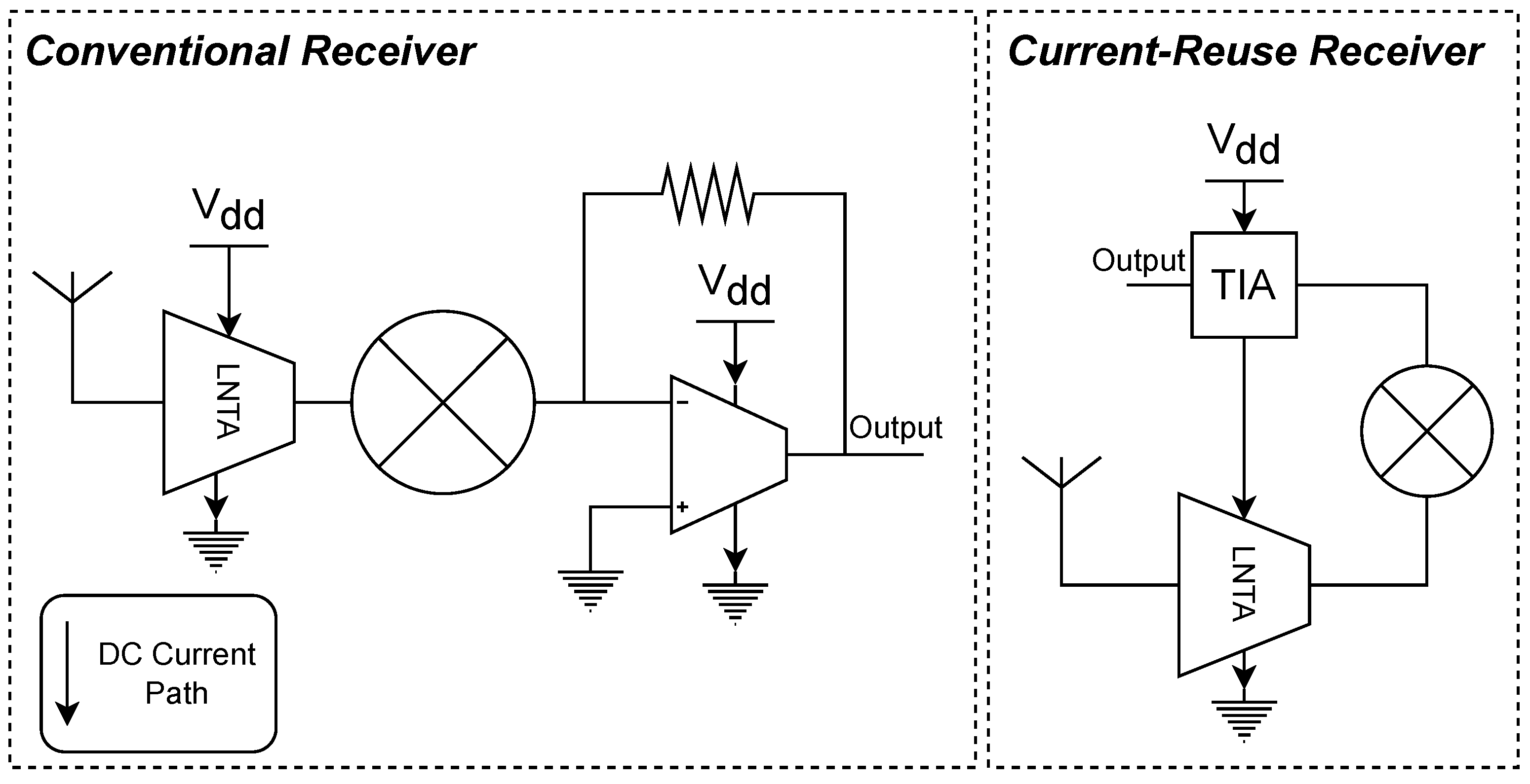
A well-known method to design low-power circuits is the current-reuse technique, which is conventionally used to design low-noise transconductance amplifiers (LNTAs) [
1]. In [
2], a push–pull LNTA is used in a cascaded receiver to reduce the power consumption. However, it reports a poor 1 dB compression point (P1dB) of
. A stacked baseband amplifier is employed in a mixer first receiver architecture in [
3] that achieves very low power consumption. However, it has limited bandwidths due to the mixer’s first architecture that makes it unsuitable for wideband modulation schemes. A quadrature low-noise amplifier (LNA) followed by poly-phase filter (PPF) is employed in [
4] to improve power efficiencies. However, it suffers form a narrow RF bandwidth due to the common-source LNA topology. Another approach in [
5], employs a current-reuse LNA followed by an on-chip LC-balun and a passive PPF to reduce the dynamic power consumption in the LO signal path. However, the combination of the on-chip LC balun followed by PPF limits the bandwidth, which is not suitable for wideband applications. In [
6], a free phase-locked loop (PLL) receiver architecture is proposed, but the reported NF of
is very high. Recently, thanks to the scaling down in CMOS technology, where the voltage threshold (
) reduced and the transition frequency (
) increased, the current-reuse technique is employed to design a receiver front-end by stacking different blocks and to share the bias current from a single supply to reduce the overall power consumption in comparison to the conventional approach in which circuits are cascaded with separate supply currents, as shown in
Figure 1.
A wide range of studies has been performed on designing low-power receivers using the current-reuse technique. The low-noise amplifier (LNA), down-conversion mixer, and voltage-controlled oscillator (VCO) are stacked in [
7] to share a single supply and bias current, which achieve very low power consumption. However, the reported NF of 10
is high. Moreover, it may suffer injection locking of the VCO. In [
8], the LNTA, active mixer, and baseband (BB) filter are cascoded. Its choice of an active mixer increases the voltage’s headroom requirement to achieve high linearity. In [
9], a function-reuse method is employed where a push–pull amplifier functions as both the LNTA and TIA. However, a low supply voltage results in a poor P1dB performance of
. Moreover, the circuit is mainly suitable for sub-GHz applications due to the limited RF bandwidth. An N-path current-reuse receiver is another alternative that is also suitable for sub-GHz applications [
10]. One of the issues in N-path receivers is the requirement for additional circuitry to combine the N paths that require additional power consumption and area. Moreover, the active mixer used requires more voltage headroom. A
noise-cancellation (NC) technique and linearity enhancement method is utilized by [
11], but it consumes a relatively high 8
. A current-reuse technique is used in [
12] by sharing the VCO current with the LNA and PA. Moreover, a function-reuse mixer is employed that reduces the overall power consumption. However, the stacking of the VCO on the LNA and PA may cause problems with VCO locking. Another approach is to employ a method of simultaneous input matching and a
NC technique that results in a very low NF of
[
13] at the cost of very limited RF bandwidth. Both current-reuse receiver (CRR) circuits proposed in [
13,
14] share the output node with the down-conversion mixer input, which causes loading and a loss of the RF signal. In our earlier works [
15,
16,
17,
18], the concept of an active-inductor (AI) and a
NC technique was introduced to overcome the problems mentioned above. The AI circuit helps isolate the output node from the mixer input. In addition, the
NC technique pushes the
noise corner below 1
.
This work mainly employs the quadrature (I/Q) low-power and wideband RF-to-BB CRR front-end proposed in [
17] to assess its functionality with different matching circuits over a wide frequency range. It evaluates the performance of the LNTA using both a differential balun without an on-chip biasing inductor and an LC balun with an on-chip biasing inductor. The RF-to-BB CRR employs both an AI and
NC to improve the gain and NF performance by isolating the RF signal from the output node and removing the common-mode low frequency noise. It utilizes a wideband cross-coupled common-gate (CCCG) topology to convert the RF voltage to an RF current, and a 25% down-conversion passive mixer is used to convert the RF current to a BB current without consuming the DC current. Finally, it converts the BB current to the BB voltage using a TIA circuit that shares the DC current with the LNTA to reduce power consumption.
This study shows that the proposed CRR is well-suited for different matching circuits over a wide RF range and discusses both input matching methods and their impact on performance. Notably, a structure with a differential balun and without an on-chip biasing inductor is studied, having a reduced area in comparison to what was proposed in [
17].
The paper is structured as follows.
Section 2 overviews the receiver front-end architecture and provides a detailed description of the front-end circuitry, and
Section 3 presents the measurement results. This is followed by a conclusion.
2. RF-to-BB-Current-Reuse Receiver Front-End Circuit-Level Considerations
Scaling down the CMOS technology node improves the frequency of operation and reduces the
of the transistors. This allows for the stacking of circuits to share the bias current using a single supply. This introduces several design challenges to maintain the overall performance, which was studied in our earlier work [
17]. In reality, designing a receiver front-end requires time and cost. It would be very efficient to design a receiver front-end that can be used for several frequency bands with minor adjustment in the input matching network. Moreover, a receiver compatible with different matching networks helps reuse the receiver for applications having different requirements.
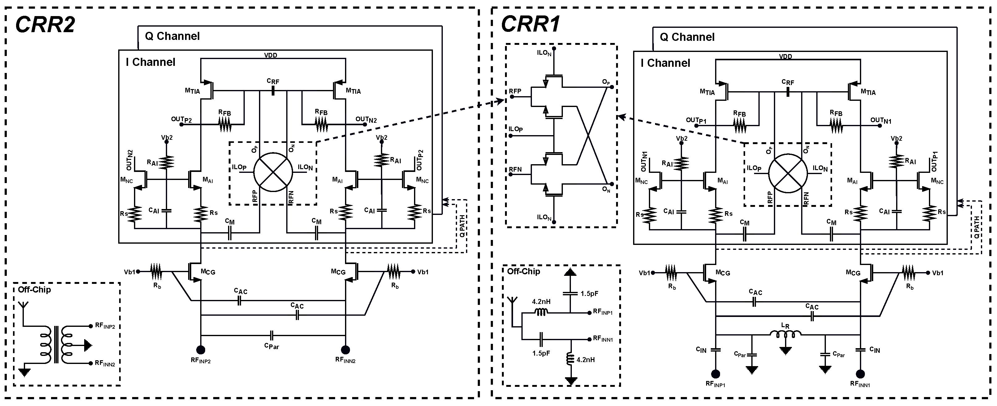
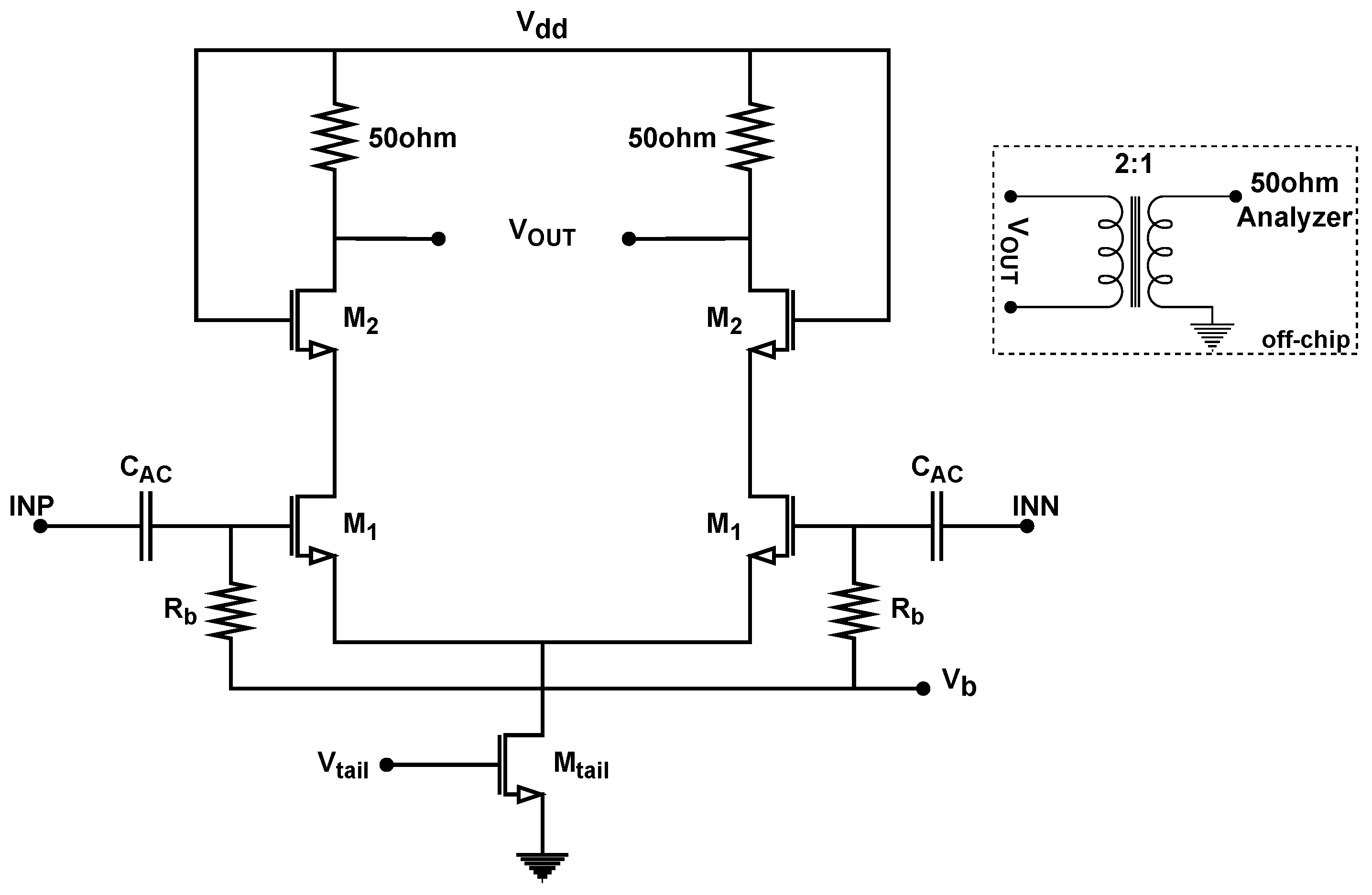
The block diagram of the circuit proposed in [
17], CRR1, and the block diagram of the proposed circuit in this work, CRR2, are shown in
Figure 2. CRR2 does not include an internal biasing inductor for the DC current path and uses an external differential balun. Both circuits include the LNTA, which mainly defines the receiver performance, the down-conversion passive mixer to reduce the DC power consumption, and the voltage headroom required; the AI and
NC circuits that are used to improve the NF performance; and the TIA that converts the BB current to the BB voltage at the output. The TIA shares the current with the LNTA to reduce the power consumption.
2.1. LNTA Design with Differential Balun and LC Balun Input-Matching Network
The LNTA is the first stage in the receiver front-end which defines the sensitivity and amplifies the weak input signal before down-conversion. There are two well-know topologies to design the LNTA circuit: the common-gate (CG) and the common-source (CS). In [
13], a common-source topology was used, which results a very low NF at the cost of narrow bandwidth. However, the CS topology is very sensitive to non-idealities such as wire-bonding, reducing the design robustness of the LNTA. On the other hand, the CG topology is well-known for its design robustness and wideband operation, but it has a higher NF. It provides input matching via
that can be achieved by optimizing the current and the W/L ratio [
19]. However, the CG topology requires high currents to achieve the required
. To overcome this issue, a cross-coupled technique is employed to boost the effective
by two times without consuming extra DC currents. This results in achieving the required input matching, NF, and gain. Moreover, this cross-coupling avoids using large transistors to achieve the required
, which results in less parasitics that reduce the RF signal losses and improve NF. In this work, a CCCG LNTA is used with wideband input matching and allows for higher robustness at the cost of higher NF.
In
Figure 2, the CCCG LNTA is formed by
and the cross-coupled connection of
. The NF is given by the following:
where
and
are the bias-dependent noise parameters, and
is the source resistance. The balun losses can be modeled by series resistor
.
is reduced by increasing the channel-length slightly but it maintains an
that is at least ten times higher than the frequency of operation.
To perform input matching using a 1:1 differential balun,
is designed for it. Then, the second term in (
1) increases by two times. The noise factor is then given by the following.
Compared to the differential balun, the LC balun converts the 50
antenna impedance to the required impedance (in this work, 25
) on the differential side. In this way, the LNTA can be designed with a higher
while maintaining the input matching performance and reducing the NF. In this way, the LNTA noise is given by the following.
The LNTA with a differential balun can be designed with a 25 input impedance but at the cost of poor input matching.
In this work, the LNTA is designed using an LC balun and a differential balun at its input in CRR1 and CRR2, respectively.
The single-ended antenna input needs to be converted to a differential signal at the input of the LNTA. CRR1 employs an off-chip LC balun to convert the single-ended signal to a differential one. Moreover, an on-chip inductor,
, is used to provide the DC current path and resonates with large parasitic capacitors,
, at the input of the LNTA.
helps reduce RF signal losses and allows the receiver to operate at higher frequencies, as will be later shown in the measurements. Although the LC balun is well-known for its narrow band operation, its combination with the CG LNTA topology provides wideband input impedance matching [
15]. Alternatively in CRR2, an off-chip single to differential balun is utilized. The balun provides the DC current path that removes the need for the on-chip inductor that requires a significant die area. However, it suffers from high RF signal losses due to the parasitic capacitances that did not resonate as in CRR1, reducing its operating frequency range capabilities.
The LC balun and LNTA in CRR1 are tuned to operate from 1 to . CRR2 is designed over a similar frequency range to compare with CRR1, but its input matching strategy will nonetheless reduce its operating frequency range.
2.2. Active-Inductor and 1/f Noise-Cancellation Technique
Conventionally, CRRs use cascode devices to boost the output impedance and isolate the I/Q paths [
13,
15]. However, they suffer from RF signal losses due to the sharing of the mixer input with the output node that has large capacitive loading. Moreover, the
noise from the LNTA is directly coupled to the output via the cascode transistor, despite the conventional receiver architecture that uses an AC-coupling capacitor before the mixer to remove low frequency components. To overcome the issues mentioned above, our earlier works [
14,
16,
17] proposed the AI and
NC circuits.
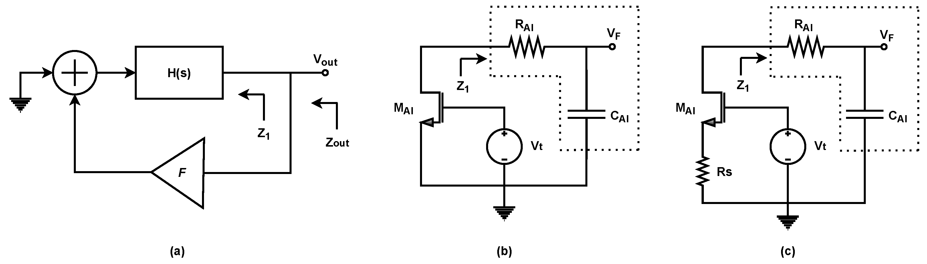
The AI circuit helps isolate the passive mixer input from the output node to avoid RF losses due to the loading of the output node, which helps improve the NF and gains at higher frequencies even in a relatively large technology node, such as 130 CMOS.
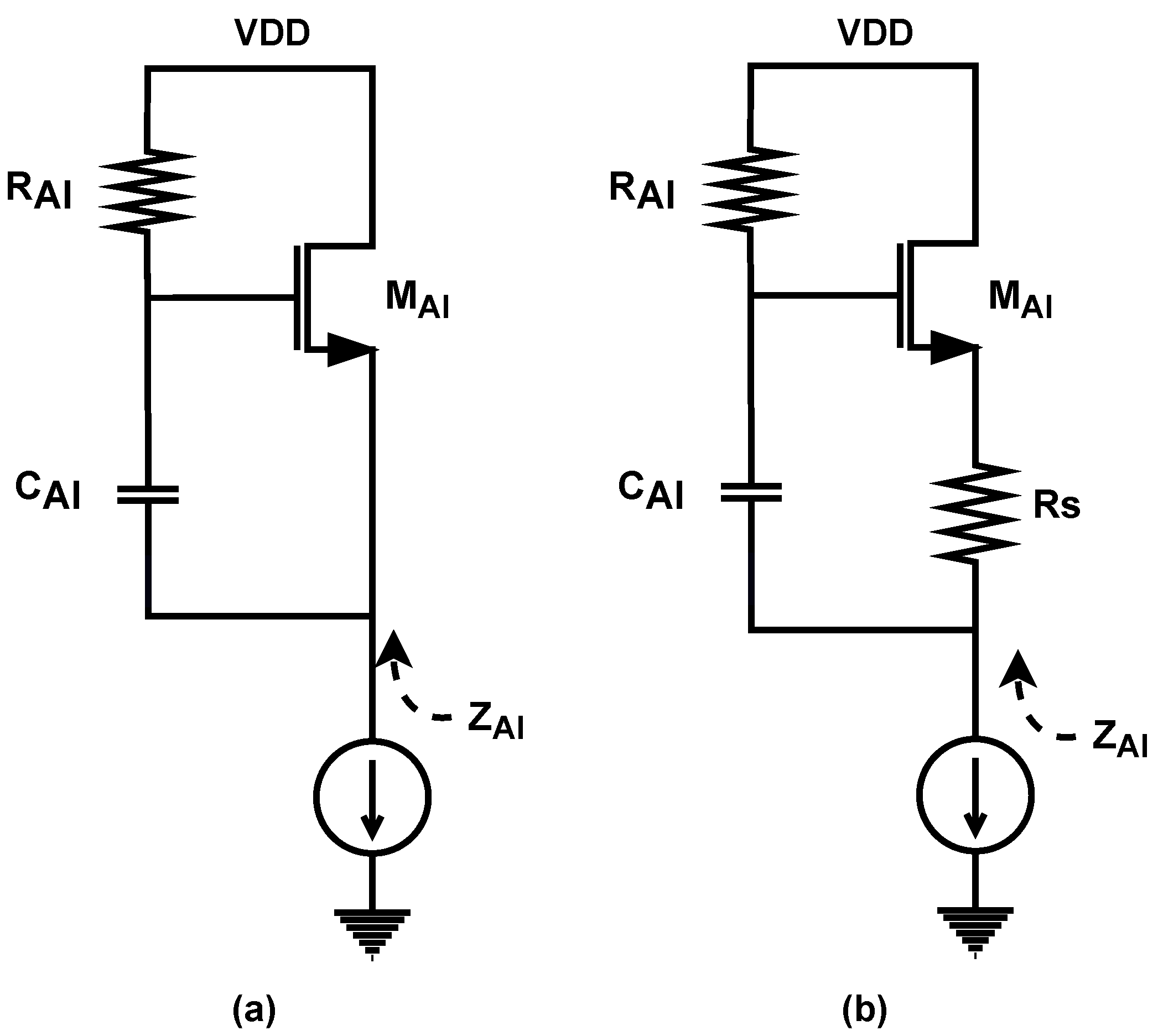
Figure 3a shows the conventional AI proposed in [
20]. The AI is formed by
,
, and
. The impedance looking into the AI circuit is small at low frequencies to pass the DC current while it kept increasing and moving towards high frequencies. The impedance with respect to the circuit shown in
Figure 3a is given by the following:
where
is the parasitic capacitance at the mixer input.
is dependant on the technology node.
A small resistor,
, is added to boost the impedance looking into the AI circuit at the cost of voltage headroom, as shown in
Figure 3b. The impedance looking into the AI circuit
is then calculated by the following.
Appendix A derives (
5). The mathematical model of
from (
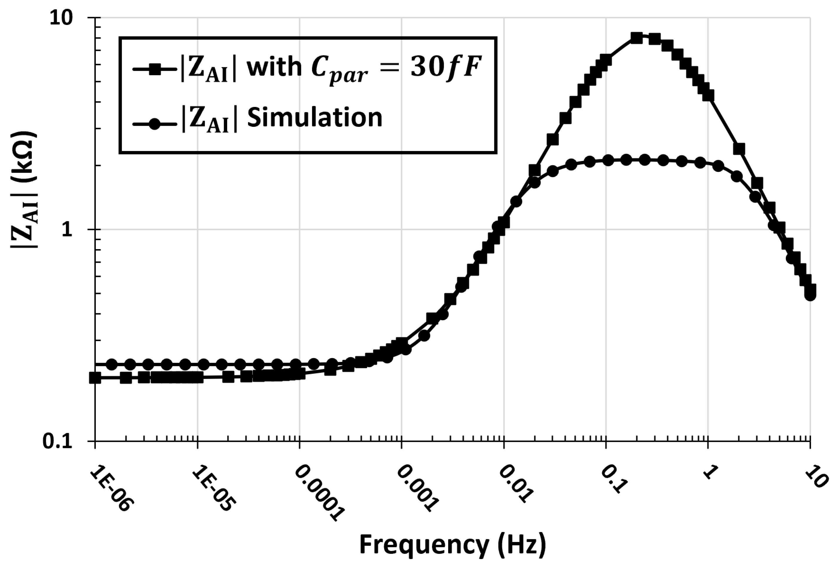
5) with a
value of 30
is plotted versus the frequency along with simulation results in
Figure 4, where
is of 3.5 mS,
is of 1
,
is of 30
, and
is of 200
. For high values of
, the low frequency impedance in (
5) is equal to
if channel-length modulation is ignored.
As mentioned previously, the LNTA noise is directly coupled into the CRR output since the AI circuit does not block low frequencies. To suppress the resulting low frequency noise, a NC circuit is used. provides the signal path to the output with the opposite sign to cancel the low frequency noise and push the corner to a lower frequency.
2.3. Passive Mixer
The RF current from the LNTA needs to be down converted to the BB current before the TIA and BB circuits. To this end, both active and passive mixer structures can be employed. Usually, the passive mixer is preferred over the active mixer since the active mixer suffers from both a voltage headroom issue and a direct coupling of low frequency noise.
Accordingly, a 25% double balanced passive mixer is employed to down convert the RF current from the LNTA to a BB current without DC power consumption and no voltage headroom limitation. The mixer should have an input impedance that is much smaller than that of the LNTA output impedance in order to ensure lower NF and higher gain. Moreover, a low input impedance reduces the voltage gain at the input of the mixer, which improves linearity. Thus, it is important to optimise switch sizes in a way that achieves low input impedance, while maintaining a sufficiently small parasitic capacitance to avoid RF signal losses. The gate of the mixer switches need to be biased such that the LO signal switches on and off the mixer completely. The voltage bias of the source and drain terminal of the mixer switches is provided by the TIA. The rail-to-rail voltage of the LO signal should not exceed the transistor breakdown, and a voltage that is similar to the supply or lower is preferred.
2.4. Transimpedance Amplifier
The TIA is formed by a single transistor,
, and feedback resistor,
. It converts the BB current to the BB voltage at the output. A large channel-length is preferred for
to enhance the output impedance. The simplified equation of the conversion gain is given by the following:
where
is two-times the transconductance of transistor
.
3. Experimental Results and Discussions
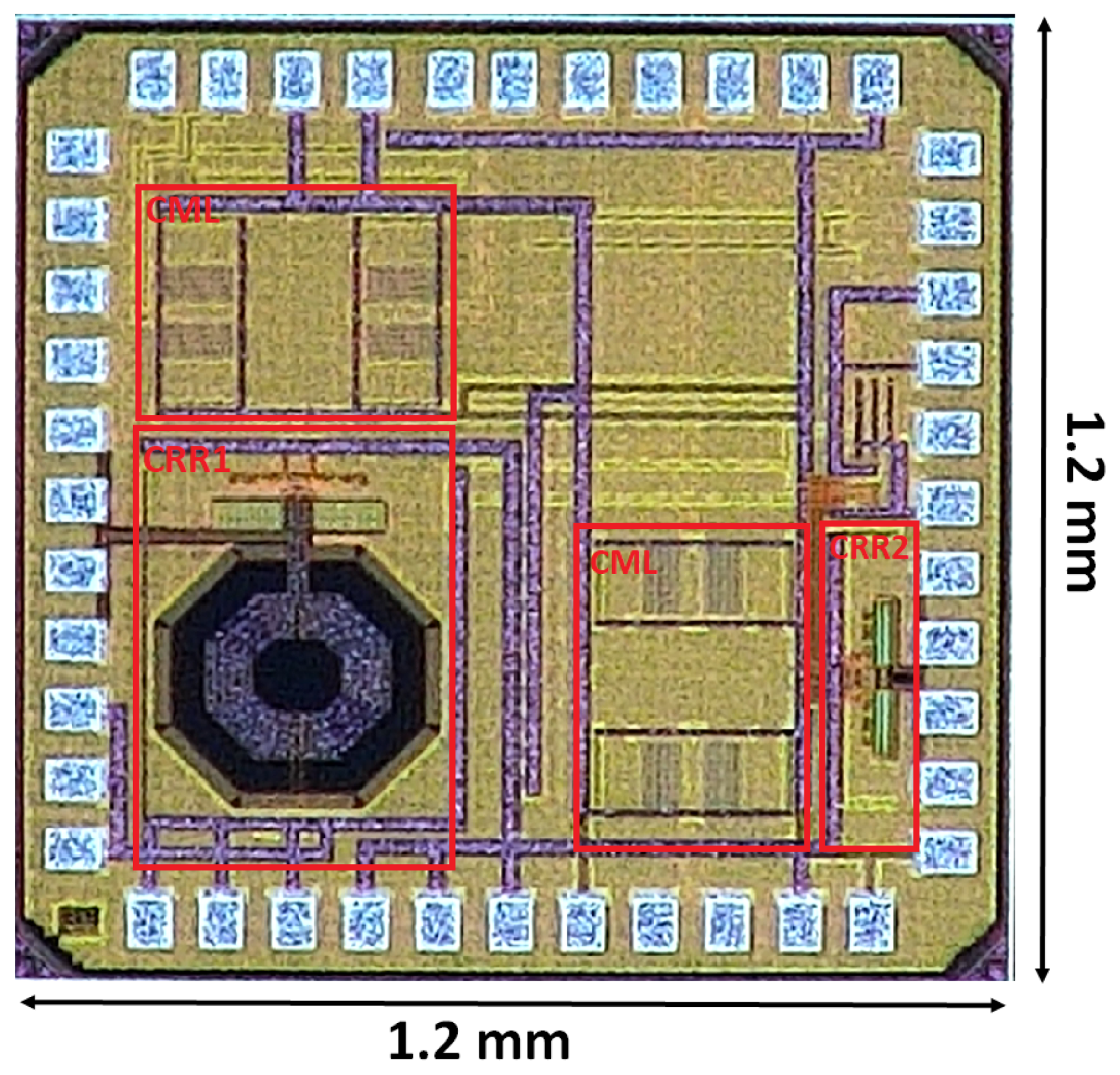
The wideband and low-power current-reuse receiver front-end was fabricated in a TSMC 130
CMOS process, and the die micrograph is shown in
Figure 5, occupying a total area of
. The on-chip current-mode logic (CML) buffer provides output matching to measure the performance of the CRR using a spectrum analyzer (Agilent N9020A), as shown in
Figure 6. The CML buffer needs to consume a high power of 48
so that the CRR performance is maintained, notably its linearity. The current bias needs to be adjusted to achieve a transconductance for
that yields a 0
gain given by
. The required transconductance can be reduced by half if the output impedance is doubled. This helps reduce the effect of parasitic capacitors and increases the bandwidth of the CML buffer. In this way, to match the 100
output impedance of the CML buffer with the spectrum analyzer, a 2:1 differential to single-ended balun is required and losses need to be taken into account during measurements. In addition, the cascode transistor,
, enhances the output impedance and reduces the miller effect to increase the bandwidth. The large AC-coupling capacitor,
, is used to separate the CML buffer biasing from the CRR’s output voltage. Both CRR and CML buffers utilize a
supply.
As previously discussed, the performance of the circuit is characterized using two different input matching networks: (i) a differential balun (TCM1-63AX-2+) and (ii) a custom-designed LC balun. This outlines the robustness of the circuit, along with its operation over a wide RF band with the two input matching methods utilized.
For this purpose, as shown in
Figure 2, two CRR topologies were implemented in this work: one with an on-chip inductor, CRR1, which occupies an active area of
and is measured using an LC balun at its input, and the other without an on-chip inductor, CRR2, that occupies a much smaller active area of 0.025
and is measured with a differential balun at its input. These active areas exclude the CML buffer and bond pads. Both CRR1 and CRR2 consume
from the
supply. This identical current biasing is selected to provide a representative comparison of both presented circuits.
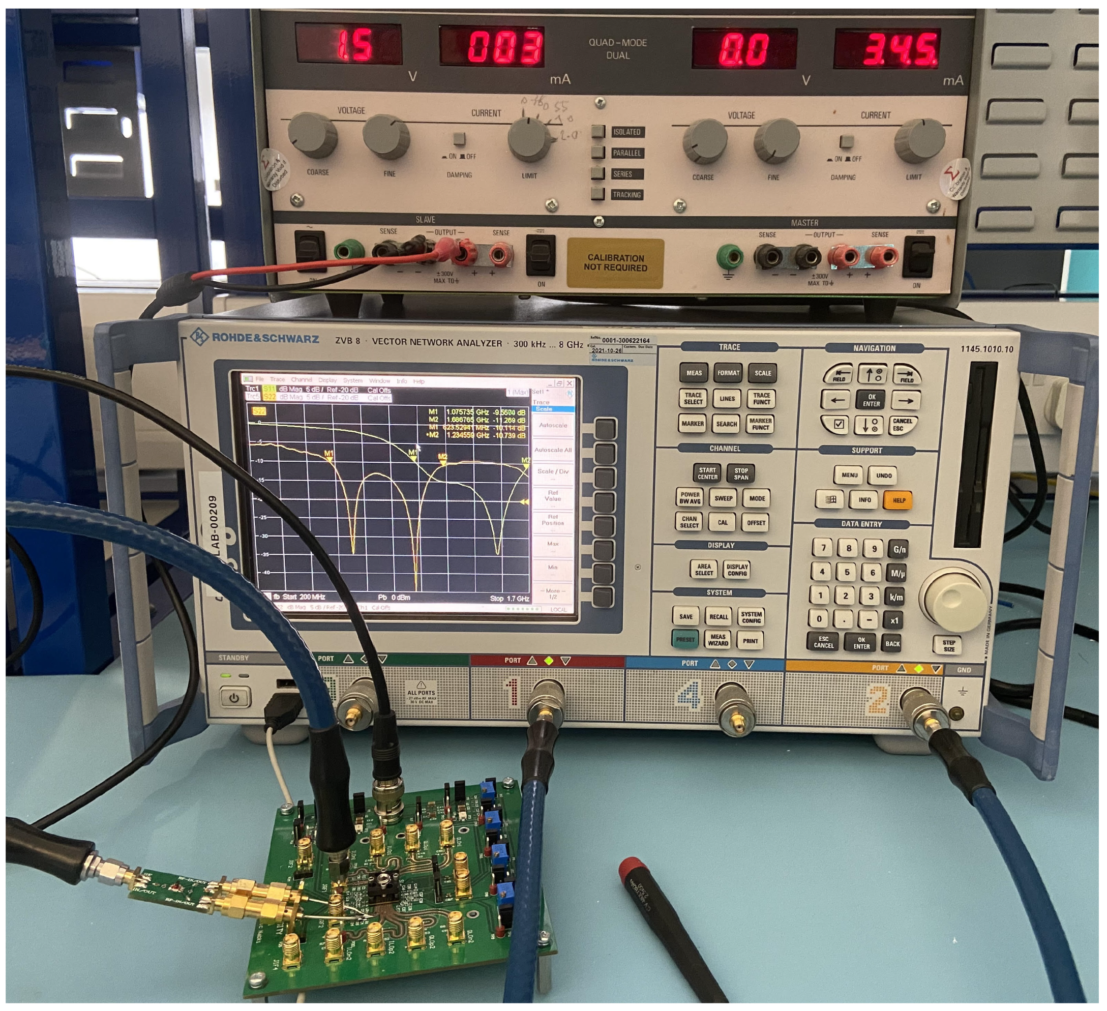
The chip is packaged in a QFN48, and it is connected to the PCB using a socket (SG-MLF-7006). Non-idealities related to the cable, socket, and external output balun are carefully considered. To this end, the S-parameter characteristics of the cables and baluns are extracted using a four-port vector network analyzer (VNA) (Rohde and Schwarz ZVB-8). The socket losses are provided by the manufacturers’ datasheet. Two signal generators (Agilent N5182a MXG) were used to generate the input signal and the clock signal for the down-conversion mixer switches. For the measurement, the differential output of the CML buffer is converted to a single-ended output to the spectrum analyzer using an external 2:1 balun.
Figure 7 shows the measurement setup using a VNA to measure the
performance of CRR1 and CRR2. The power supply shows that both CRR1 and CRR2 consume 3
together while their CML buffers powered down.
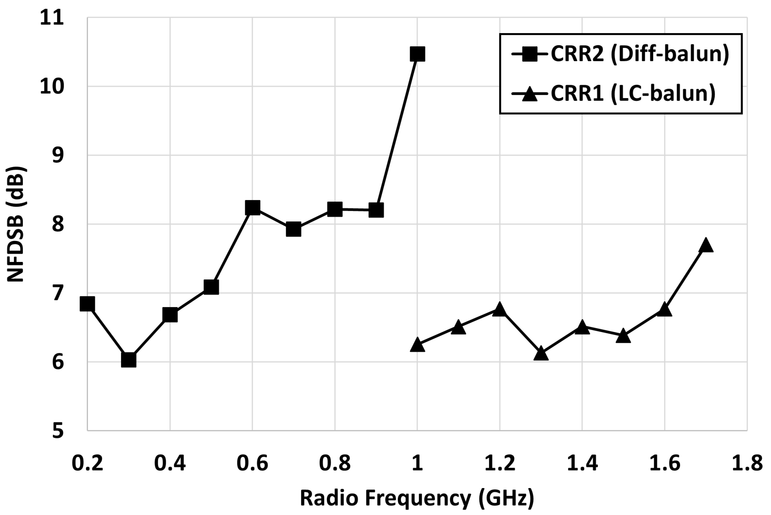
There are several methods to measure the NF performance of the receiver. In this work, the Y-factor method, which utilizes a noise source, is employed with high accuracy. The NF performance of CRR1 and CRR2 is measured across the RF input and is shown in
Figure 8. The NF remains below 8
over the RF from 1 to
in CRR1. However, the NF is increasing from 6 to
with the RF proceeding from
to 1
in CRR2. This is thanks to the on-chip inductor used in CRR1 that resonates with
at the frequency of operation, which reduces RF signal losses and allows CRR1 to maintain its NF performance at higher frequencies. However, this comes at the cost of a larger chip area for CRR1 due to its on-chip inductor. The performance of both CRR1 and CRR2 is verified across the IF while the LO frequency is constant at
and
, respectively, and the results are shown in
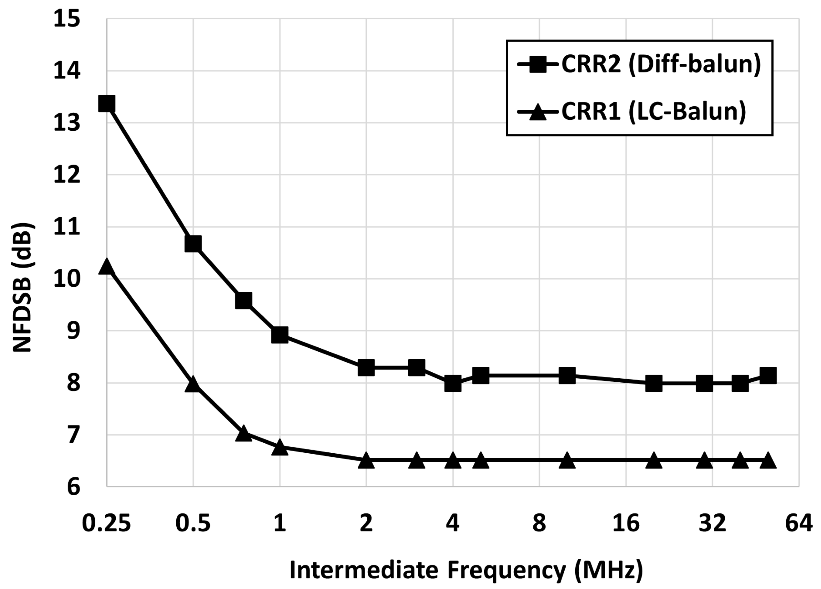
Figure 9. The low frequency noise is suppressed and the
corner noise is pushed to a low frequency of less than 1
thanks to the
NC circuit.
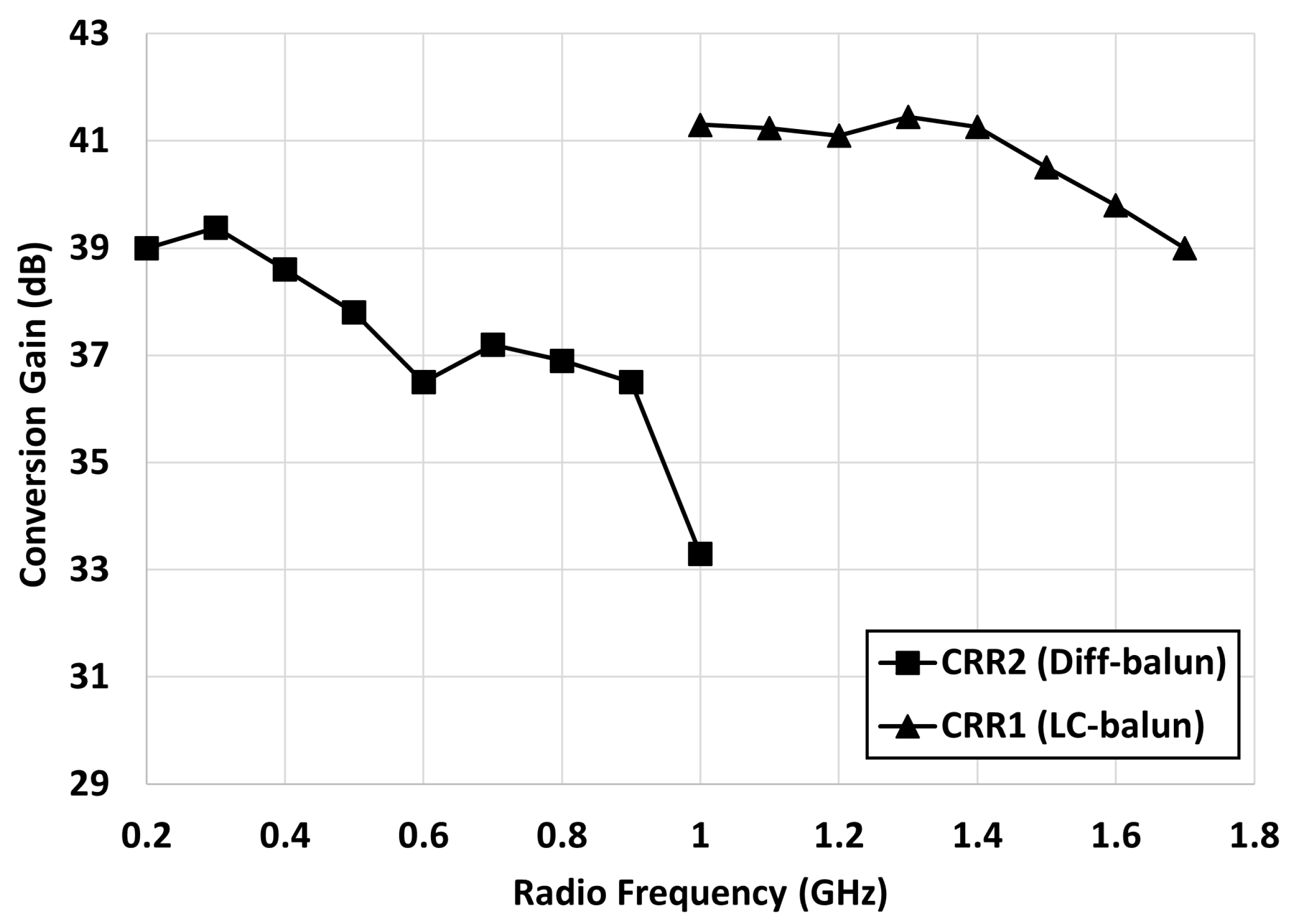
A low-power RF signal with a 5
frequency spacing from the LO frequency is applied to the input to calculate the conversion gain from the output signal power at BB (in dBm) minus the power of the input signal at RF. The measured conversion-gain performances versus the RF input is shown in
Figure 10. Relative to the NF performance shown in
Figure 8, the conversion gain in CRR2 reduces from
to 33
over the RF input range from
to 1
while CRR1 maintained its conversion-gain performance of about 40
over the entire RF band from 1 to
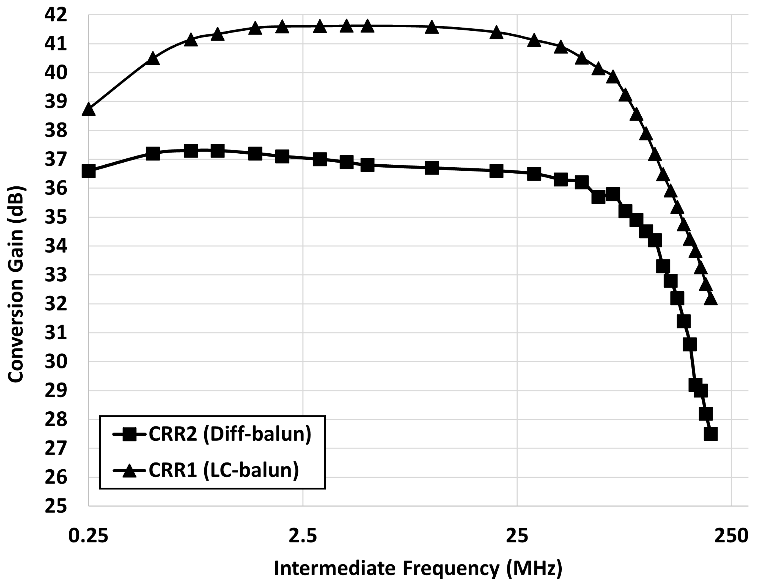
. The conversion-gain performance is also measured across the IF while the LO is constant at
in CRR1 and
in CRR2. The resulting conversion gain curves are plotted in
Figure 11. The bandwidths of both CRR1 and CRR2 remain almost the same since they use the same AI,
NC, passive mixer, TIA, and CML buffer. In this figure, CRR1 achieves almost
-higher gain than CRR2 due to the higher loss of the differential balun and the lack of on-chip inductor to resonate with the paracitic capacitors at the input of the receiver.
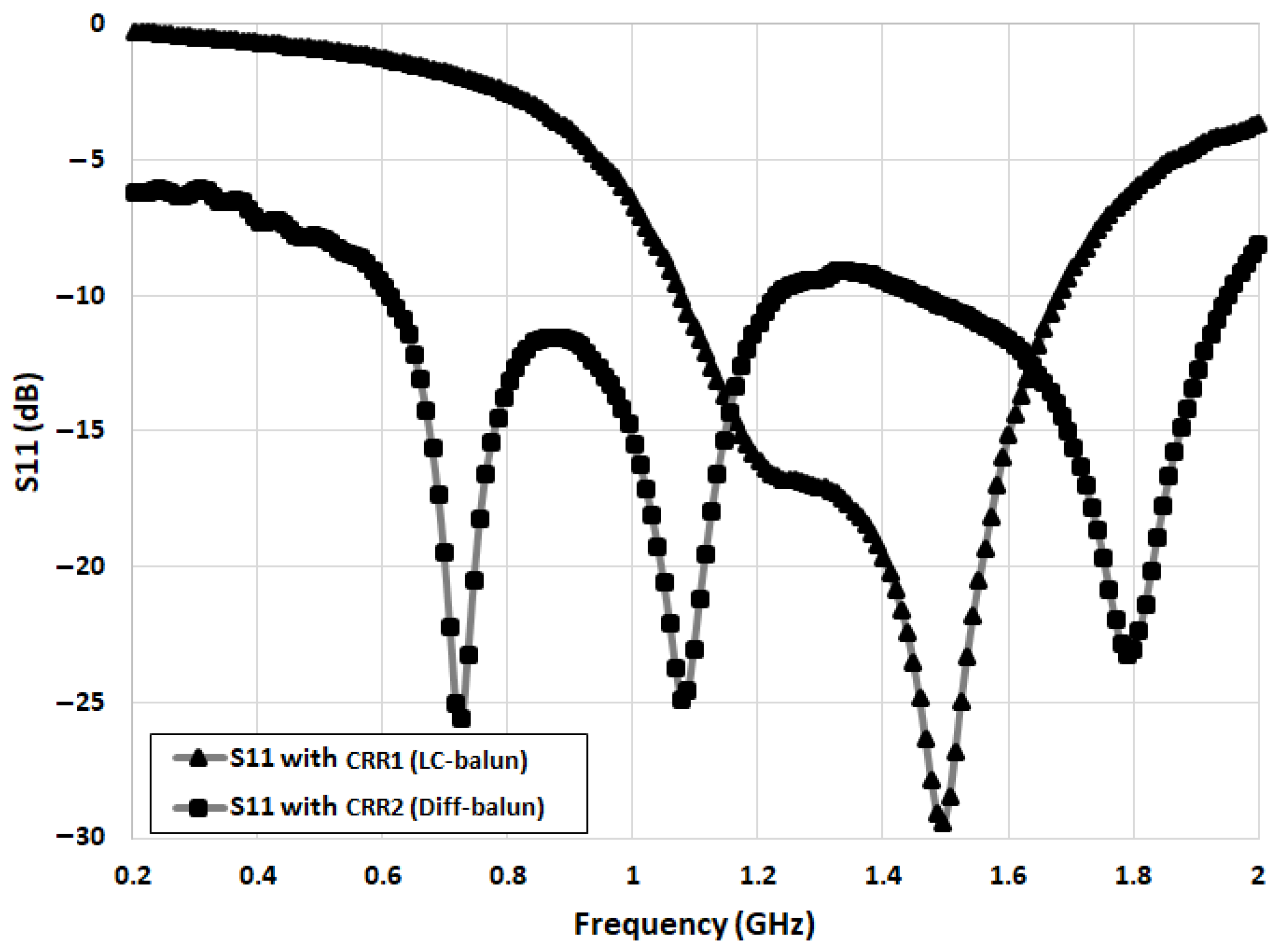
The
performance of both CRR1 and CRR2 is measured versus the RF input using a VNA, and the results are shown in
Figure 12. It illustrates that CRR1 with the LC balun achieves an
<
over a wide RF bandwidth from
to
. CRR2 achieves an
<
over a band of
to
. Although
is higher than
for frequencies below
in CRR2, due to the reduced parasitic capacitor contribution at lower frequencies, resulting in reduced RF loss, it could nonetheless maintain a good NF and conversion gain. At
, the
is
, which is equivalent to the a mismatch-induced loss of
.
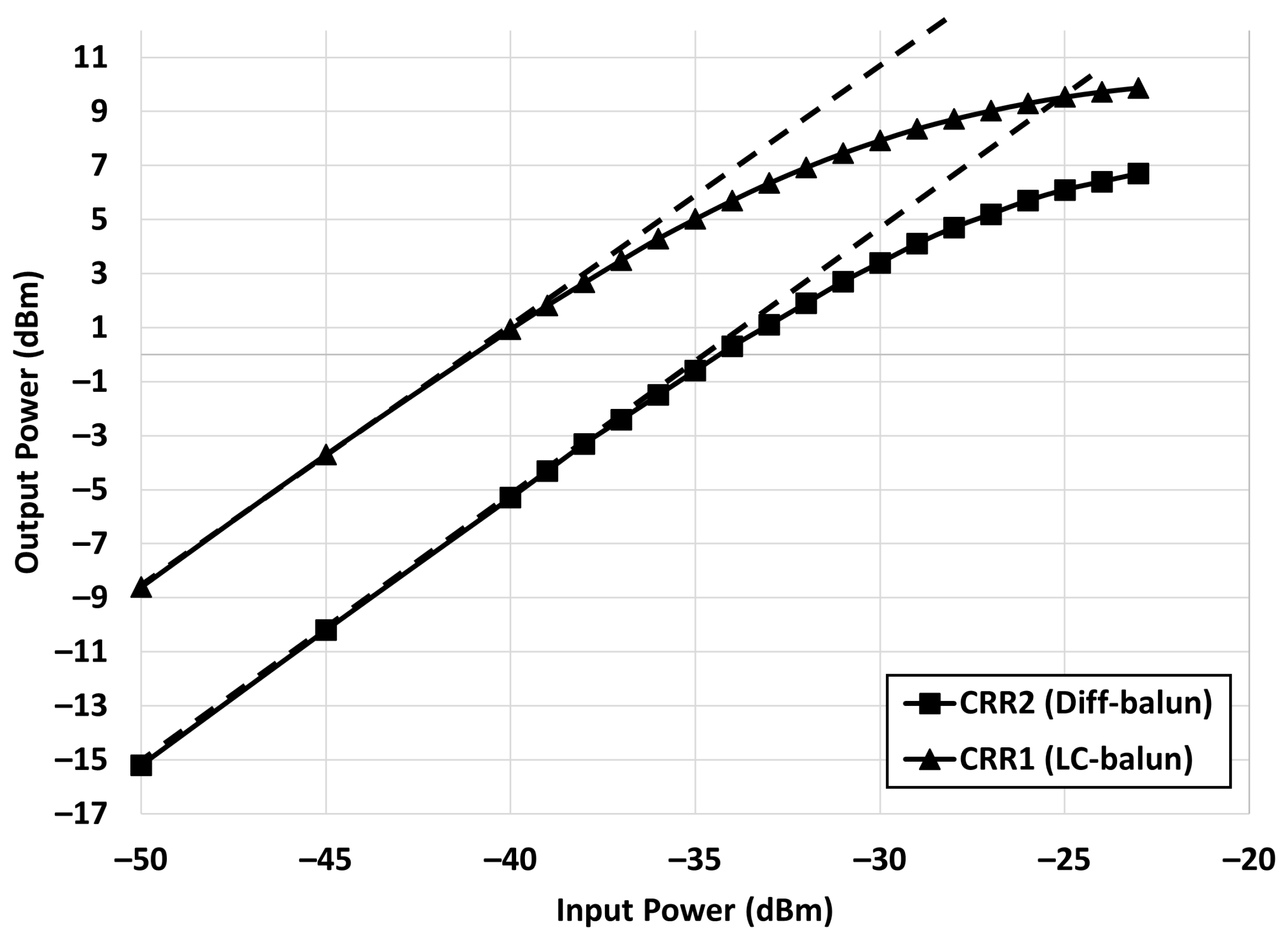
The linearity performance of CRR1 and CRR2 is characterized using P1dB and the in-band third-order intercept point (IIP3). The P1dB measurement is performed by applying a single input tone that is 5
offset from the LO signal, where the signal power is swept from
to
. This is performed when the LO signal is at
in CRR1 and
in CRR2. The resulting output power versus the input power is plotted in
Figure 13. It shows that CRR1 achieves an input P1dB of
, while CRR2 achieves a higher input P1dB of
, which is relative to the gain difference reported above.
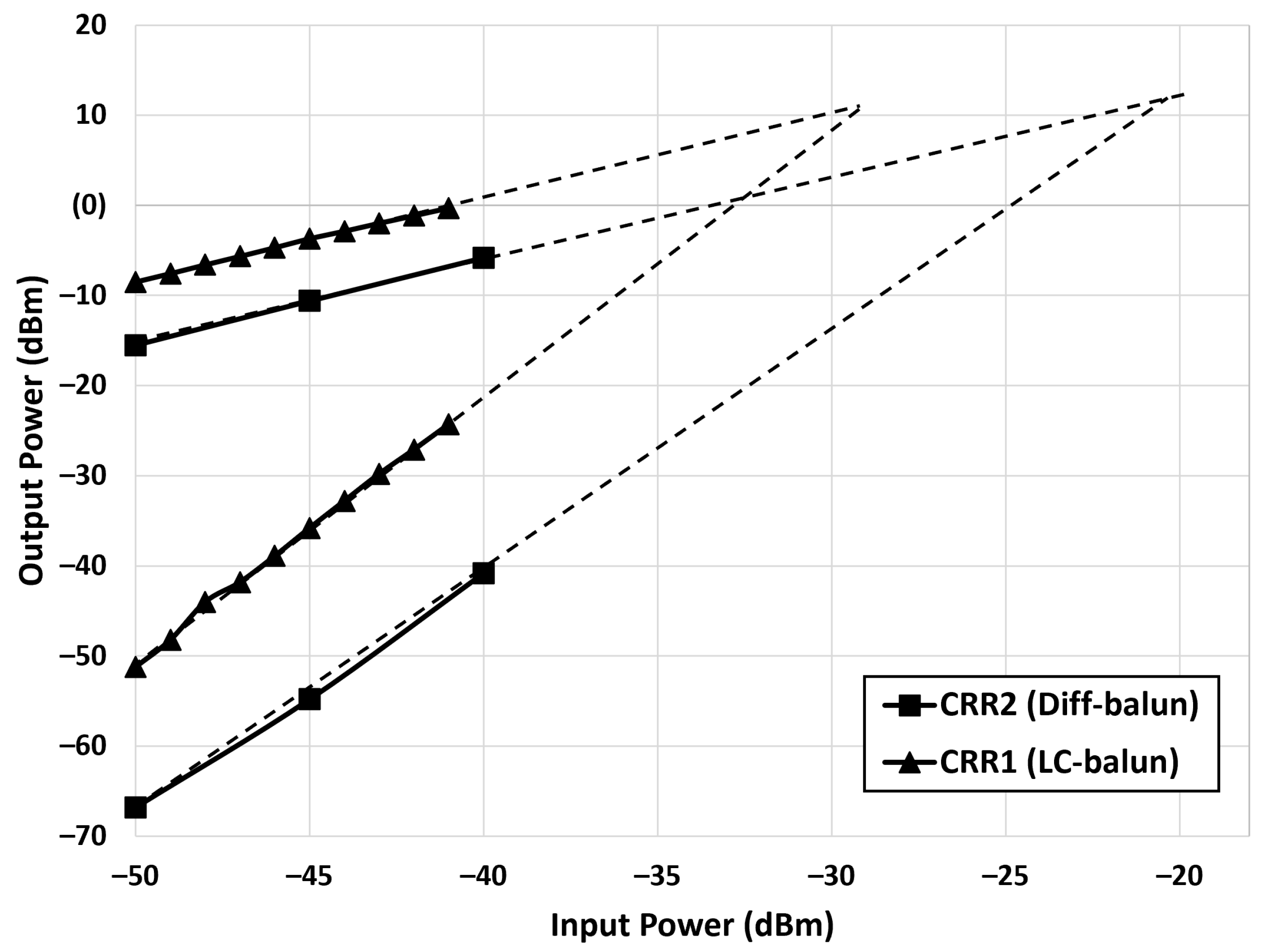
The IIP3 performance is evaluated using a two-tone test applied to the input with 10
and 11
offsets from the LO signal, while the LO frequency is at
in CRR1 and
in CRR2. The input power swept from
to
. This generates two fundamental tones of 10
and 11
along with two intermodulation products of 9
and 12
at the output. The output fundamental tone and the third-order intermodulation products are plotted versus the input power in
Figure 14. It illustrates that CCR1 achieves an IIP3 of
, while CRR2 achieves an IIP3 of
. Note that there may be a few
s of uncertainty in the IIP3 results since the CML buffer may limit the linearity.
The overall performance summary of CRR1 and CRR2 along with a comparison to other works using a current-reuse topology is reported in
Table 1. The results show that CRR2 operates at lower frequency compared to CRR1 in our earlier work. Otherwise, the overall performance remains similar. Notably, in CRR2, the conversion gain is reduced and the NF increased, but linearity is improved. Moreover, CRR2 achieves a higher bandwidth of 110
compared to CRR1 ( 90
).
Overall, this circuit topology, in either of the forms presented, achieved a high BB bandwidth, making it suitable for wide modulation bandwidth applications. The NF, IIP3, and bandwidth performances compare well with the state-of-the-art methods considering the power consumption and technology node of the presented receivers.
The presented architecture shows that it can provide good performance metrics regardless of the input network selected for impedance matching. An LC balun input matching strategy (CRR1) shows that a more uniform gain and NF can be obtained at the cost of added inductor die area. CRR2 exhibits more conversion gain and NF variations over its operating frequency range, and it has a lower frequency of operation, but it requires significantly reduced active areas (the lowest reported in the table), which can be an advantage in some applications.


