1. Introduction
The arrival of the “big data” era has put forward higher requirements for data processing. Modern high-performance processors have been able to complete real-time processing of large amounts of data, but real-time transmission of large amounts of data is also required between processors or between peripherals and processors. Therefore, higher and higher requirements have also been placed on the interface. Due to the parallel interface facing serious problems such as crosstalk and noise (SSN) in high-speed data transmission, the high-speed serial interface has become the mainstream transmission method. Today’s high-speed serial link usually uses SerDes (Serializer and Deserializer) technology [
1,
2], That is, high-speed serial data for data transmission between chips or boards.
As data transfer rates increase, signal integrity issues become increasingly prominent. Due to the non-ideal characteristics of the channel, the high-speed data sent by the transmitter (Tx) is attenuated and inter-symbol interference (ISI) exists after passing through the channel, and the data received by the receiver has been seriously distorted. In order to recover the data correctly, an equalizer is required to recover the channel attenuation and the inter-symbol interference. However, due to temperature, power-supply changes, and differences in channel materials and lengths, the equalizer usually uses self-adeptive algorithms to compensate for the attenuation of the different frequency components of the signal. In the literature [
3], periodic calibration is performed by means of a preset protocol to update the DFE coefficients. In this way, although the tap coefficient of the equalizer can be converged to the optimum, the transmission efficiency of the signal is reduced due to the periodic transmission of redundant signals. In the literature [
4], in order to reduce the equalization intensity, a 5-tap feedforward equalizer of the transmitter is used in combination with the channel to generate a duobinary signal. However, a data-driven feed-forward equalizer (FFE) at the TX does not help to reduce jitter amplification. Moreover, performing adaptive equalization at the transmitting end requires additional algorithms to solve the synchronization problem at the transmitting and receiving ends.
In order to meet the requirements of fast and accurate equalization of high-loss channels, the Serdes equalizer designed in this paper adopts the method of combining digital and analog equalization. Analog equalization is carried out by a two-stage continuous-time linear equalizer (CTLE), which provides equalization and gain just below the Nyquist frequency. This equalization combined with partial channel loss can be used for DB signal generation while reducing the performance requirements of the subsequent analog-to-digital converter (ADC). The data sampled by the 64-channel ADC is sent to the 16-tap FFE and the 1-tap pre-decision decision feedback equalizer (DFE) for adaptive equalization processing, which further improves the signal quality of the receiver. Compared with digital DFE, the realization of digital FFE equalization is simple and compact, and the requirements for timing are more flexible. Signals of the duobinary type have proven to be very efficient modulation formats on high-loss channels. In order to reduce the overall equalization strength and reduce the bandwidth required by the receiver, this paper adopts a new generation method of DB-PAM4 and a joint adaptive algorithm. The DB-PAM4 signal is not directly generated at the transmitting end, but uses the roll-off characteristic of the channel itself and then is adjusted by the adaptive CTLE to produce the effect of binary processing. The rest of this article is divided into three parts. The second part describes the overall architecture of the equalizer, including the analysis and implementation of the DB-PAM4 signal. The third part introduces the key technology of the adaptive equalizer. The fourth section is the experiment and verification of the algorithm. The last is the conclusion of this paper.
2. The Principle and Realization of the Adaptive Equalizer
2.1. Adaptive-Equalizer Overall Architecture
The DB-PAM4 signal is a special seven-level modulation signal. Due to the limitation of the output voltage, de-emphasis is often used to equalize the transmitter, resulting in a reduction in the total voltage swing. When the equalizer is not used at the transmitter, the transmitter becomes simpler, avoiding the additional complexity introduced by FFE at the transmitter and relaxing the linearity specification of the transmitter. Moreover, amplifying the signal at the receiving end is more conducive to power optimization in later designs.
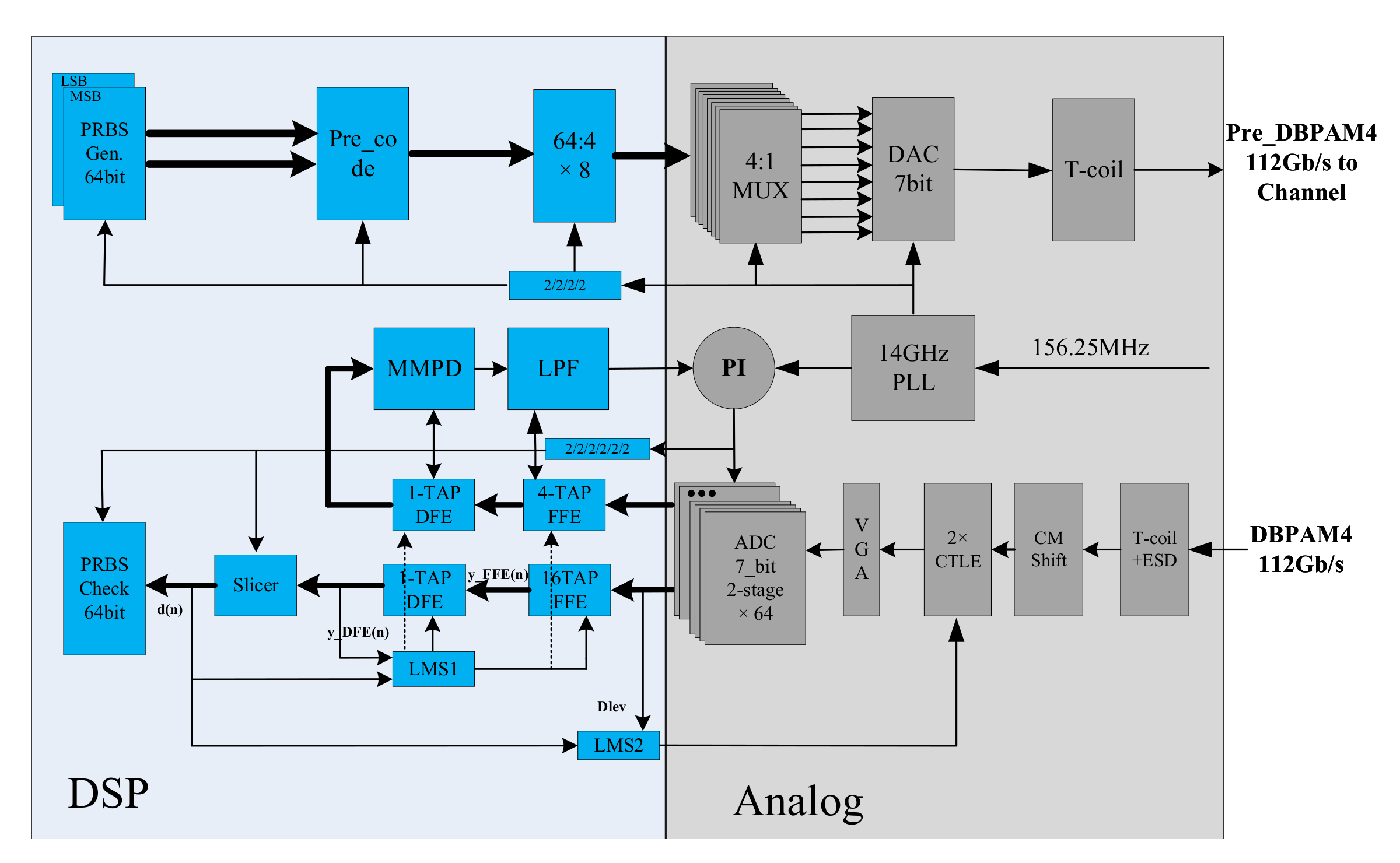
Figure 1 shows the overall-architecture block diagram of the adaptive equalizer. In order to reduce power consumption and meet the requirements of high-loss channels, this paper adopts a new DB-PAM4 generation method and joint adaptive algorithm. The equalizer mainly works at the receiving end. The transmitter uses a PRBS generator to generate a 64-bit digital signal and then modulates the data into a Pre-PAM4 signal at low speed to avoid erroneous transfer when generating a DB-PAM4 signal. The receiver data uses a T-coil to enhance input matching. A subsequent common-mode conversion stage boosts the input common-mode voltage from 550 mv to the CML level with some peaking. This is followed by a two-stage CTLE to eliminate long-tail ISI, reducing the number of taps in the FFE while increasing the SNR at the ADC input. After the VGA adjusts the signal amplitude, the ADC samples the analog signal into 64 parallel 7-bit digital signals. The DSP is composed of a 16-tap FFE and a one-tap DFE, and the operating frequency is 875 M to deal with the residual ISI that is not equalized by CTLE.
2.2. Theoretical Analysis and Implementation of Adaptive Equilibrium
At a transmission rate of 112 Gb/s, the half-baud rate attenuation of PAM4 signal modulation through backplane communication reaches at least −30 dB. It is difficult for traditional equalization methods to effectively compensate for such a large channel attenuation. In this paper, the new DB-PAM4 transmission method is adopted, and the duobinary coding of the entire channel is realized by adjusting the equalization strength of the equalizer at the receiving end. This method includes part of the channel loss, the required equalization intensity is reduced, and the bandwidth requirement is reduced.
The equalization processing is divided into two steps: the first step is pre-equalization, which tests and shapes the unknown channel to adapt to the duobinary processing results. The second step is digital equalization, which is to finely adjust the tap coefficients of the digital equalizer to reduce the bit error rate of data transmission. The two-step adjustment method greatly improves the adaptability of the adaptive equalizer. Compared with the traditional method of adding redundant channels or protocols, the processing method in this paper greatly reduces the hardware overhead and ensures the accuracy of the equalization results.
2.2.1. Pre-Equalization Process
Duobinary uses known intersymbol interference to reduce the required channel bandwidth [
5], which makes it a specific form of the partial response signal. Specifically, the current symbol is added to the previous symbol through a delay filter:
.
Figure 2a shows the power spectral density of the PAM4 signal at the transmitter, The DB-PAM4 signal is generated at the receiver by shaping the total channel response into the form
.
Figure 2b shows the single impulse response through the DB channel.
Figure 2c shows the power spectrum of the signal at the receiving end, the bandwidth of which is reduced to half of the original signal [
6]. In
Figure 3, the red curve shows the power spectrum of the ideal DB channel, but it is obviously unrealistic to shape the full frequency band for a low-pass actual channel, so we use a low-pass filter to fit the DB channel. As shown by the blue line in
Figure 3, with the combination of channel and CTLE is this type of Bessel low-pass filter [
7], the processing result of the DB channel can also be satisfied. Although the high-frequency signal is lost, it is more conducive to implementation.
Since the 112 Gb/s PAM4 signal has a similar power spectrum to the 56 Gb/s NRZ signal, and the latter is more conducive to judging whether the DB channel is generated at the receiving end, we use the NRZ signal for processing in the pre-equalization stage. When the transmitter sends an NRZ signal, the receiver will generate three levels through the DB channel, and these level transitions do not include the highest-to-lowest direct transition. Using this feature, the unknown channel can be converted into a DB path, and the pre-equalization process is shown in
Figure 4. The transmitter sends a 56 Gb/s NRZ signal (equivalent to only sending the highest and lowest levels of pre-PAM4), and when it reaches the receiver through the channel, the “2” “1” and “0” signals are judged by the decider and the error signal is calculated.
In order for the algorithm to actually be implemented, certain information must be constrained. Since the ideal levels of “2” and “0” are uncertain until CTLE stabilizes, and the DB signal is symmetrical about the middle level, the error when dropping the “2” and “0” signals will not affect the convergence accuracy of the algorithm, and the symbol value is used instead of the ideal level of the output. The error signal
e(n) is:
The updated formula for the bias voltage dlev is expressed as [
8]:
Since the eye diagram is completely closed at the beginning of the algorithm, and the error is large, in order to avoid CTLE over-equalization and ensure the reliability of adjustment, DFE is added to the algorithm. The DFE of 1 tap mainly provides the determined symbol value and error for the algorithm. In addition, the initial value of the DFE tap starts from 0. The ideal resistance value of CTLE to adapt to the DB channel and the initial tap coefficient of DFE can be obtained through adjustment. After stabilization, the output result of the DB channel is shown in the lower right corner of
Figure 4. The eye diagram of the receiver can clearly see the DouBinary eye diagram.
2.2.2. Digital Equalization Process
After pre-equalization, the data path was made to roughly satisfy the DB processing. At this time, the parameters of CTLE are fixed, and the DFE equalization value is used as the initial value of the next stage. In order to avoid error transmission during data transmission, precoding is required for DB-PAM4 data [
7]:
, bk precoded signal; ak is the original PAM4 signal. The precoded signal still belongs to the PAM4 type signal, and its corresponding z-domain expression is:
.
At this time, although the data path has undergone pre-equalization processing, the quality of the DB-PAM4 signal received at the receiving end is very poor, and a digital equalizer needs to be used for further data recovery. The digital equalization process is shown in the DSP part of
Figure 1. The 64-channel parallel data sampled by the ADC is digitally processed by the 16-tap FFE and then enters the 1-tap pre-decision DFE for further equalization. The whole digital equalization part adopts the LMS algorithm for self-adaptive adjustment. The clock frequency of the digital part is 875 M. The specific design of digital equalization is explained in detail in the next chapter.
3. Circuit Design
3.1. Tunable CTLE Equalizer with Complementary Symmetric Structure
Due to the low-pass characteristics of the channel itself, the analog equalization module at the front end of the receiver plays a very important role, and its equalization directly determines the effect of DB processing. CTLE is essentially a high-pass filter whose function is to compensate for the channel bandwidth while generating a roughly Doubinary channel through adaptive adjustment. In a high-loss channel of −35 dB, CTLE should provide about 16 dB of equalization strength. The traditional CTLE with a source-level degenerate CML structure composed of only NMOS cannot provide a large gm, which often leads to insufficient equalization strength. In this paper, CTLE with a complementary symmetrical structure is used to improve the gain and linearity of the equalizer. The complementary gm circuit shown in
Figure 5a consists of PMOS and NMOS differential transistor pairs to increase the total gm.
and
are the transconductance of the input NMOS transistor and PMOS transistor, respectively. When
, the CTLE output function of the complementary symmetric structure is expressed as [
9]:
Compared with the CTLE of the conventional structure, the high-frequency gain is improved by about two times. Although this complementary topology requires a higher supply voltage, the power dissipation can be reduced by 1/2 because the same current flows through the NMOS and PMOS transistors. This scheme requires a 20% higher supply voltage than the NMOS-only scheme to keep both devices in saturation. Combining lower currents with higher supply voltages results in power savings of about 40%. Since the DB-PAM4 signal can compress the signal energy to low frequencies, CTLE can provide equalization slightly below the Nyquist frequency. Through Matlab simulation analysis, the equalization frequency of CTLE is at [0.4–0.5] × fband, which reduces the design difficulty of analog equalization. As shown in
Figure 5b, the output of the resistor array is controlled by an adaptive algorithm to achieve adjustable equalization strength. The capacitor array can be manually controlled. However, under the high-speed data of 112 Gb/s, when the data frequency at the receiving end does not change, the degradation capacitance value Cs does not change.
3.2. The FFE Adaptive Circuit
The FFE circuit is the core of the digital equalizer, providing about 16 dB of equalization strength for the entire equalization system.
Figure 6 is a block diagram of the 16-tap parallel FFE structure, 64 parallel 8-bit input data are combined into a 78 × 8 array, in which D0–D2 is the data of the previous clock cycle, and D66–D78 is the data of the next clock cycle, which is used to match the tap coefficient setting of the FFE. Due to the relative symbol characteristics of DB-PAM4 signals, a controllable forward intersymbol interference is used for signal generation; therefore, in the FFE circuit design of this paper, there are only 3 forward taps, 1 main tap and 12 post-item taps. The 78 × 8 data array uses shift multiplication in addition to obtaining 20-bit data. Finally, the upper 12 bits of the reserved data are used in subsequent DFE circuits. The LMS-based adaptive FFE tap coefficient update can be expressed in vector form as [
10]:
In the formula,
is the tap coefficient of the
i-th tap;
is the error signal output by DFE; and
is the ideal value after judgment. For 16-tap, the 64-way parallel data formula can be expressed as:
3.3. DFE Adaptive Circuit
DFE is a nonlinear equalizer, which is composed of a feedback filter and a Slicer, which can eliminate the ISI of the current symbol to the subsequent symbols, and has a better compensation effect on the reflection and fluctuation of the channel. However, the power consumption of DFE is larger than that of FFE under the same number of taps. In this paper, only one-tap DFE is used as equalization to reduce the error signal. Due to the high transmission rate, this paper adopts a pre-decision DFE to solve the problem of tight timing in the feedback loop. The traditional DFE structure needs to complete the calculation and decision process in the feedback loop, while the pre-judgment DFE only selects the MUX unit in the feedback loop [
11]. After the pipeline structure is adopted in the whole data path, the pre-determined DFE is more suitable for high-speed circuits and parallel data chains.
The structure of the DFE is shown in
Figure 7. After the decision value of the decider passes through the feedback filter, it is differentiated from the input signal and directly eliminates the ISI from the input signal. The decision value is output by the Slicer.
Similar to FFE tap update, the DFE tap update can be expressed as [
10]:
The overall equalization intensity of the DFE is relatively small, and it provides about 5 dB of equalization intensity in the overall equalizer, so the convergence speed can be relaxed under the premise of ensuring its convergence accuracy. Therefore, each time the DFE tap coefficients are updated, only one set of numbers needs to be randomly selected as the parameters required for the result equalization. Its update algorithm can be expressed as:
4. Test Results
Figure 8 shows the pre-equalization test platform. The pre-equalization test platform iwass built using the laboratory’s bit error tester, adjustable CTLE receiver chip, and FPGA. The NRZ data of 56 Gb/s is sent by the bit error tester, respectively, through the 50 cm and 85 cm long backplane channels, and input to the receiver chip. The external FPGA controls the adaptive algorithm to self-adjust the CTLE’s degradation resistance Rs and DFE tap coefficient. As shown in
Figure 9 and
Figure 10, after stabilization, the output control signals dlev are 23 and 16, respectively, and the controlled resistance values are 350
and 700
, respectively.The tap coefficients of the DFE are 10 and −7, respectively.
Figure 11 is the test result displayed by the oscilloscope. After adjustment, you can see the obvious Doubinary signal. Channel reshaping is complete.
On the cadence IC software platform, the circuit was built as shown in
Figure 1, the analog part adopts TSMC 28nm technology, the DSP is generated by Verilog, and the extracted actual channel parameters are used as channel parameters for further verification. The pre-equalization results are consistent with the test results, and the second step adjustment results are as follows;
Figure 12 shows the LMS algorithm for DFE and FFE coefficients at 112 Gb/s −35 dB. Due to the pre-equalization process, after the algorithm is started, the tap coefficient of FFE can be stabilized within 6 us, while the convergence speed of DFE equalization is slow and stable within 10 us. After the AMS simulation, the DSP output result is redrawn to the eye diagram. The result is shown in
Figure 13. It is obvious that six open eyes can be seen, and the bit error rate of the system is 3e-9.
Table 1 summarizes the performance of the DSP and compares it with the DSPs of other PAM4/DB-PAM4 receivers operating above 112 Gb/s. The two-step equalization method greatly reduces the equalization intensity; compared with other structures of DSP, the system has fewer taps at 112 G high-speed data and has obvious advantages in bit error rate and hardware overhead. In the 28 nm CMOS process, it can achieve performance similar to that of the advanced process. Compared with the literature [
12], with the same technology, the design of digital DSP is more convenient to transplant, and the processing capability in high-loss channels is stronger. The adaptive adjustment algorithm makes the receiver more adaptable to the channel.
Figure 14 shows the system layout of the digital DSP part.
5. Conclusions
The main purpose of this paper is to apply adaptive equalizers to SerDes receivers. On the 112 Gb/s high-loss channel (greater than 30 dB), the signal transmission method adopted in this paper can effectively reduce the signal bandwidth and reduce the equalization strength required by the receiving end. The two-step equalization method effectively improves the convergence accuracy of the algorithm, and in the pre-equalization stage, accurate reception of the signal at the receiver is not required, and the algorithm has strong robustness. Compared with high-end processes, the equalizer can achieve comparable performance.
Author Contributions
Z.W.: Conceptualization, Methodology, circuit design and simulation. M.L.: Methodology, Software. F.L.: Software, Conceptualization. X.H.: Software, circuit design and simulation. All authors have read and agreed to the published version of the manuscript.
Funding
This research was funded by National Key R&D Program of China under Grant 2018YFB2202302.
Conflicts of Interest
The authors declare no conflict of interest.
References
- Ali, T.; Chen, E.; Park, H.; Yousry, R.; Ying, Y.M.; Abdullatif, M.; Gandara, M.; Liu, C.C.; Weng, P.S.; Chen, H.S.; et al. 6.2 A 460mW 112Gb/s DSP-Based Transceiver with 38 dB Loss Compensation for Next-Generation Data Centers in 7 nm FinFET Technology. In Proceedings of the 2020 IEEE International Solid-State Circuits Conference-(ISSCC), San Francisco, CA, USA, 16–20 February 2020; pp. 118–120. [Google Scholar] [CrossRef]
- Jin, Z.; Wu, G.; Wang, C.; Chen, J. Inter Symbol Interference Correction Based on Zero-forcing Equalization for Time Interleaved Photonic Analog to Digital Converters. In Proceedings of the 2018 Conference on Lasers and Electro-Optics (CLEO), San Jose, CA, USA, 13–18 May 2018; pp. 1–2. [Google Scholar]
- Toifl, T.; Menolfi, C.; Ruegg, M.; Reutemann, R.; Dreps, D.; Beukema, T.; Prati, A.; Gardellini, D.; Kossel, M.; Buchmann, P.; et al. A 2.6 mW/Gbps 12.5 Gbps RX with 8-Tap Switched-Capacitor DFE in 32 nm CMOS. IEEE J.-Solid-State Circuits 2012, 47, 897–910. [Google Scholar] [CrossRef]
- Verplaetse, M.; De Keulenaer, T.; Vyncke, A.; Pierco, R.; Vaernewyck, R.; Van Kerrebrouck, J.; Bauwelinck, J.; Torfs, G. Adaptive Transmit-Side Equalization for Serial Electrical Interconnects at 100 Gb/s Using Duobinary. IEEE Trans. Circuits Syst. Regul. Pap. 2017, 64, 1865–1876. [Google Scholar] [CrossRef]
- Lee, J.; Chen, M.-S.; Wang, H.-D. Design and Comparison of Three 20-Gb/s Backplane Transceivers for Duobinary, PAM4, and NRZ Data. IEEE J.-Solid-State Circuits 2008, 43, 2120–2133. [Google Scholar] [CrossRef]
- LaCroix, M.A.; Chong, E.; Shen, W.; Nir, E.; Musa, F.A.; Mei, H.; Mohsenpour, M.M.; Lebedev, S.; Zamanlooy, B.; Carvalho, C.; et al. 8.4 A 116 Gb/s DSP-Based Wireline Transceiver in 7 nm CMOS Achieving 6 pJ/b at 45 dB Loss in PAM-4/Duo-PAM-4 and 52 dB in PAM-2. In Proceedings of the 2021 IEEE International Solid-State Circuits Conference (ISSCC), San Francisco, CA, USA, 13–22 February 2021; pp. 132–134. [Google Scholar] [CrossRef]
- Saber, M.G.; Gutiérrez-Castrejón, R.; Alam, M.S.; Xing, Z.; El-Fiky, E.; Xu, L.; Cavaliere, F.; Vall-Llosera, G.; Lessard, S.; Plant, D.V. 100 Gb/s/λ Duo-Binary PAM-4 Transmission Using 25 G Components Achieving 50 km Reach. IEEE Photonics Technol. Lett. 2020, 32, 138–141. [Google Scholar] [CrossRef]
- Lee, J.; Lee, K.; Kim, H.; Kim, B.; Park, K.; Jeong, D. A 0.1-pJ/b/dB 1.62-to-10.8-Gb/s Video Interface Receiver With Jointly Adaptive CTLE and DFE Using Biased Data-Level Reference. IEEE J.-Solid-State Circuits 2020, 55, 2186–2195. [Google Scholar] [CrossRef]
- Thulasiraman, D.; Gaggatur, C.G.N.J.S.; Reddy, K.S.S. A 18.6 fJ/bit/dB Power Efficient Active Inductor-based CTLE for 20 Gb/s High Speed Serial Link. In Proceedings of the 2019 IEEE International Conference on Electronics, Computing and Communication Technologies (CONECCT), Bangalore, India, 26–27 July 2019; pp. 1–6. [Google Scholar] [CrossRef]
- Nekouei, F.; Talebi, N.Z.; Kavian, Y.S.; Mahani, A. FPGA implementation of LMS self correcting adaptive filter (SCAF) and hardware analysis. In Proceedings of the 2012 8th International Symposium on Communication Systems, Networks Digital Signal Processing (CSNDSP), Poznan, Poland, 18–20 July 2012; pp. 1–5. [Google Scholar] [CrossRef]
- Roshan-Zamir, A.; Elhadidy, O.; Yang, H.; Palermo, S. A Reconfigurable 16/32 Gb/s Dual-Mode NRZ/PAM4 SerDes in 65-nm CMOS. IEEE J. -Solid-State Circuits 2017, 52, 2430–2447. [Google Scholar] [CrossRef]
- Ye, B.; Sheng, K.; Gai, W.; Niu, H.; Zhang, B.; He, Y.; Jia, S.; Chen, C.; Yu, J. A 2.29 pJ/b 112Gb/s Wireline Transceiver with RX 4-Tap FFE for Medium-Reach Applications in 28 nm CMOS. In Proceedings of the 2022 IEEE International Solid-State Circuits Conference (ISSCC). IEEE, San Francisco, CA, USA, 20–26 February 2022; Volume 65, pp. 118–120. [Google Scholar]
- Krupnik, Y.; Perelman, Y.; Levin, I.; Sanhedrai, Y.; Eitan, R.; Khairi, A.; Shifman, Y.; Landau, Y.; Virobnik, U.; Dolev, N.; et al. 112-Gb/s PAM4 ADC-Based SERDES Receiver With Resonant AFE for Long-Reach Channels. IEEE J.-Solid-State Circuits 2020, 55, 1077–1085. [Google Scholar] [CrossRef]
- Im, J.; Zheng, K.; Chou, A.; Zhou, L.; Kim, J.W.; Chen, S.; Wang, Y.; Hung, H.-W.; Tan, K.; Lin, W.; et al. 6.1 A 112Gb/s PAM-4 Long-Reach Wireline Transceiver Using a 36-Way Time-Interleaved SAR-ADC and Inverter-Based RX Analog Front-End in 7 nm FinFET. In Proceedings of the 2020 IEEE International Solid-State Circuits Conference-(ISSCC), San Francisco, CA, USA, 16–20 February 2020; pp. 116–118. [Google Scholar] [CrossRef]
| Publisher’s Note: MDPI stays neutral with regard to jurisdictional claims in published maps and institutional affiliations. |
© 2022 by the authors. Licensee MDPI, Basel, Switzerland. This article is an open access article distributed under the terms and conditions of the Creative Commons Attribution (CC BY) license (https://creativecommons.org/licenses/by/4.0/).


