Article

A New Non-Isolated High-Gain Single-Switch DC–DC Converter Topology with a Continuous Input Current

by
Hossein Gholizadeh
1 and
Lazhar Ben-Brahim
2,*
1
Faculty of Electrical Engineering, Shahid Beheshti University, Tehran 25529, Iran
2
Department of Electrical Engineering, Qatar University, Doha 2713, Qatar
*
Author to whom correspondence should be addressed.
Electronics 2022, 11(18), 2900; https://doi.org/10.3390/electronics11182900
Submission received: 16 August 2022 / Revised: 6 September 2022 / Accepted: 8 September 2022 / Published: 13 September 2022
(This article belongs to the Special Issue Feature Papers in Industrial Electronics)

Abstract

:
An ultra-high step-up, non-isolated DC–DC converter with a continuous input current was developed as a result of this research. This converter’s architecture consists of a voltage multiplier cell (VMC), a positive output super lift Luo converter (POSLLC), and a quadratic boost converter (QBS) (also referred to as a cascaded boost topology (CBT)). Thus, the bold points of the topologies mentioned earlier enhance the voltage gain of the proposed topology. It is important to note that when the duty cycle is at 50%, the converter attains a voltage gain of ten. Additionally, the constant input current of the topology reduces the current stress on the input filter capacitor. This converter’s topology was investigated and studied under various operating conditions: ideal and non-ideal modes, as well as continuous and discontinuous current modes (CCM/DCM). The converter’s efficiency and voltage gain were also compared to those of newly proposed converters. PLECS and MATLAB software tools were used in the investigation of the proposed topology. A 200 V/200 W prototype was constructed. The experimental results validated the theoretical study and the simulation results. The extracted efficiency was 91%.

1. Introduction

There are two basic topologies for DC–DC converters: isolated and non-isolated types [1,2,3,4,5]. The isolated types use a high-ratio high-frequency transformer to boost the voltage gain of the converter [6,7,8,9]. Furthermore, the transformer makes galvanic isolation between the source and the load and therefore better safety than the non-isolated converters [7]. However, using transformers increases the current stress on the switches and necessitates snubbers, which adds to the complexity, EMI noises, volume, and bulk [8]. As a result, non-isolated converters are a better alternative when the load does not need to be isolated from the source [9]. Theoretically and in an ideal case, the simple boost converter can increase its input voltage for all duty cycle values. However, in practical and non-ideal cases, high-duty cycle values dramatically reduce the efficiency and increase the voltage/current stresses on semiconductors. Furthermore, a substantial duty cycle percentage diminishes the diode’s activation time. It is important to know that the diode’s reverse recovery time prevents the diode from being quickly triggered. Consequently, the high-duty cycle is not appropriate for increasing the voltage gain in a simple boost converter. Therefore, other boost topologies are required for high step-up converters [10,11,12,13,14,15,16,17]. Other traditional structures that address some of the drawbacks of the boost converter are the Cuk, SEPIC, and Zeta converters. While the Cuk converter offers continuous input and output currents, the SEPIC converter only offers a continuous input current, and the Zeta topology offers a continuous output current. However, when employing a moderate duty cycle, these converters are unable to increase the voltage gain [1,2,3,4,5,6,7,8,9].
Given the aforementioned rationale, the optimal duty cycle should be around 50%. Thus, in this study, the various topologies will be examined and compared at a 50% duty cycle.
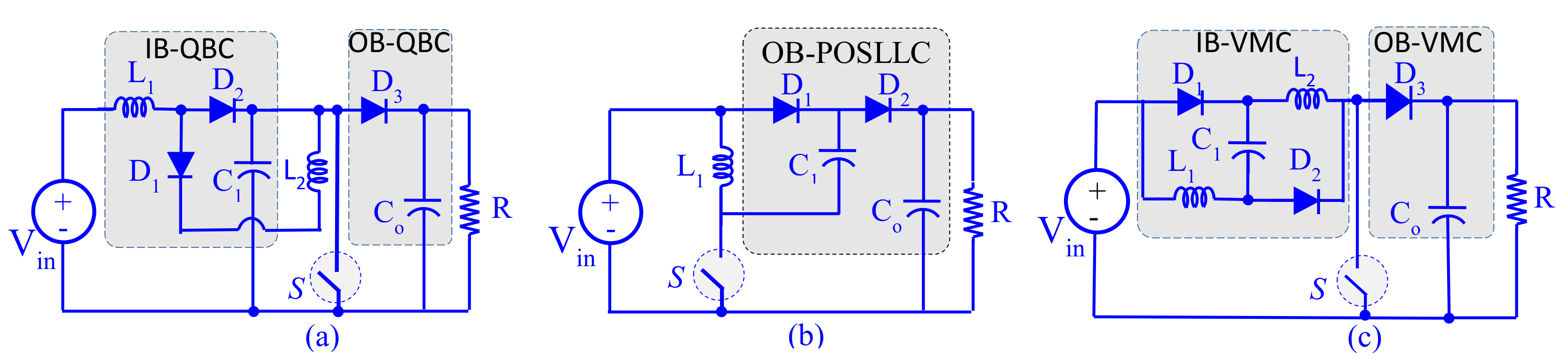
The CBT is a cascaded boost converter, also called a quadratic boost converter (QBC), and is one of these high-gain step-up converters [5,6]. The topology of QBC is illustrated in Figure 1a, it has an input block (IB-QBC) where the input inductor L 1 makes the current drawn from the source smooth. The output block (OB-QBc) is the voltage output filter. When the duty cycle is 50%, the converter provides a voltage gain of four. A ten-times voltage gain requires a higher duty cycle in this converter. The positive output super lift Luo converter (POSLLC), shown in Figure 1b, is another type of step-up converter topology with the continuous input current. Its output block (OB-POSLLC) is composed of two diodes and two capacitors. The ripples in the input current are an issue. We should mention that the voltage gain of the POSLLC is three at the 50% duty cycle. This converter cannot provide a high (i.e., ten) voltage ratio when using a lower duty cycle. The other high gain converter’s topology is a voltage multiplier cell (VMC) boost converter; the topology is illustrated in Figure 1c. The input block (IB-VMC) and the output block (OB-VMC) are clearly shown. A voltage ratio of four is obtained for a 50% duty cycle, which is similar to the CBT. The input current continuity is notable, but its ripple is high [1,2,3,4,5,6,7,8,9].
The power electronics that researchers have recommended improve topologies due to the shortages of classic topologies. Reference [18] combined the modified boost and POSLLC. The input current continuity remained. However, the use of POSLLC led to an input current ripple increase. The number of semiconductors is another issue in this topology. In other words, two switches are used (besides the three diodes). However, using two switches and more diodes decreases the converter’s reliability. We should note that the driving circuits of the MOSFETs are not the same. In other words, one switch is low-sided, and the other is high-sided. A seven-time voltage gain is the result of a 50% duty cycle. The proposed topology in [19] involves a two-switch and three-diode topology. The first inductor of this topology provides the input current continuity. This topology combined the modified boost and classic buck–boost topologies. Such a combination brings the reversed polarity of the output voltage. The voltage gain can provide higher voltage gains besides the duty cycle increasing from 50%. Additionally, the output voltage is four times more than the input voltage, while the duty cycle is 50%. Reference [20] proposed another two-switch–three-diode topology. It combines the modified forms of the boost and POSLL converters. The voltage gain for a 50% duty cycle is the same as [18]. The input current is continuous and appropriate for renewable energy applications. The lack of common ground between the input source and load is an issue in this topology. References [21,22,23] used quadratic boost structures. Reference [21] used two classic boost topologies. Both boost converters were stacked, and their stacked forms were combined. Such a topology lost the input current continuity. Consequently, the input filter capacitor suffers from dramatic high current stresses. Two MOSFETs and two diodes were the semiconductors used in this topology. A four-time voltage ratio was the result of a 50% duty cycle. Reference [22] proposed another quadratic boost topology. It increased its voltage by replacing the MOSFET of the conventional boost topology with an improved part. However, such an improved part led to a dramatically high diode voltage stress. The number of each component type was the same as in [21]. Reference [23] proposed another quadratic boost topology, combing boost, and Cuk topologies. The number of each component type was 2. Consequently, a low number of components were used. The same with [22], i.e., the second diode withstood a higher voltage than the output voltage. Notably, higher duty cycle percentages provided higher voltage gains in [21,22,23]. Reference [24] proposed a high step-up voltage gain based on VMC and a voltage doubler cell (VDC). The base topologies of VMC and VDC (improved) are classic boost topologies. Consequently, the input current was continuous, and the common ground between the input source and load remained. This topology provides a six-time voltage gain by a 50% duty cycle. Reference [25] introduced a simple cascade connection of two boost converters and a VDC. Consequently, it could increase its input voltage to eight times more than itself, while the duty cycle is 50%. This converter uses the boost topologies in the CBT form. The authors of [26] suggested an improved topology of POSLLC. The provided voltage gain provides a five-time voltage gain, while the duty cycle is 50. The input current is continuous. However, the inrush currents of capacitors have increased the input current ripple. Reference [27] recommended another one-switch topology. The conventional buck–boost converter is the base of this topology. Notably, a VMC was replaced with the base topology inductor. Due to base topology shortages, the input current was not continuous. Additionally, the output voltage was reversed. The duty cycle was 50%, and the provided voltage gain was 3. Therefore, the duty cycle must approach unity to provide higher voltage gains. Reference [28] combined a VMC and VDC with a classic boost converter. Therefore, the resulting voltage gain with a 50% duty cycle was eight times. Using VMC instead of the boost converter’s inductor increased the input current ripple. Reference [29] used two various VMCs with the conventional boost. The improved VMC was replaced with the converter’s inductor. Notably, the input current ripple increased due to the mentioned replacement. Reference [30] combined two conventional boost topologies, VMC and POSLLC. The mentioned VMC was replaced with the inductor of the first boost topology. Consequently, the input current ripple increased. Moreover, the employed POSLLC at the second part led to another inrush current. Notably, the proposed converter in [30] provides a 10-times voltage ratio with a 50% duty cycle.
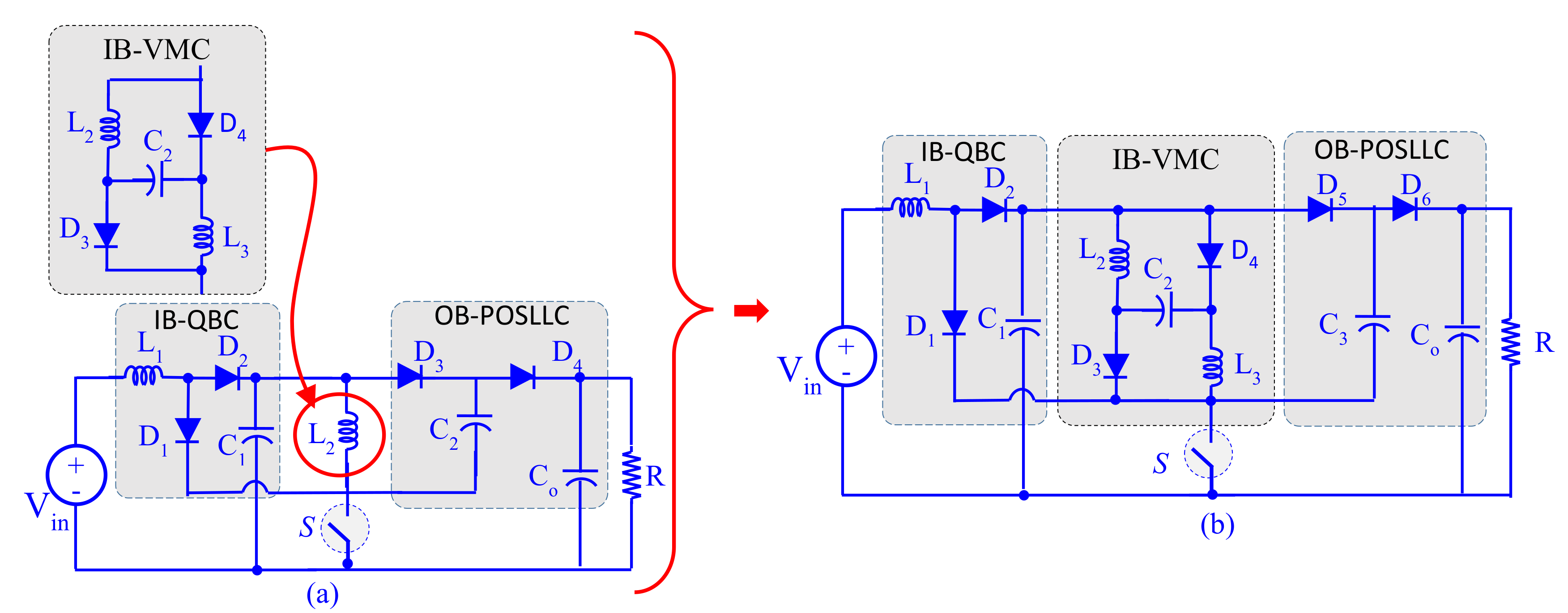
In this paper, a new topology is proposed to reach a voltage gain of 10 times at a 50% duty cycle. The composition of the proposed ultra-high step-up non-isolated DC–DC topology is depicted in Figure 2a. It is something of a cross between CBT, POSLLC, and VMC topologies, making it suitable as a high step-up converter. The complete circuit of the proposed topology is shown in Figure 2b. The proposed topology has the combined features of the three topologies. The CBT or QBC topology can increase its input voltage to four times when its duty cycle is 50%. Additionally, the POSLLC and VMC use the voltage lift technique to provide a higher voltage gain. The proposed topology is based on all three mentioned converters. CBT is the fundamental part of the proposed converter, and its various blocks have been improved by incorporating the POSLLC, which replaces the output block of the CBT (OB-QBC). In this case, there are two choices to use the VMC: (1) the VMC substitutes the inductor L 1 or L 2 of Figure 2a. Substituting L 1 will increase the input current ripples while substituting the inductor L 2 leads to an increase in the voltage gain and continuity of the input current. The proposed topology is therefore based on the latter approach (see Figure 2b), which employs a double voltage lift technique, allowing for a very high-voltage gain while ensuring input current continuity and small ripples.

2. Ideal and Continuous Current Mode of Converter

The proposed new topology of DC–DC converters is capable of providing a ten-times voltage ratio at a 50% duty ratio. As the front part is a CBT (see Figure 2a), the suggested converter draws a constant current from the source. As a result, the difficulties in the input filter design are overcome. 
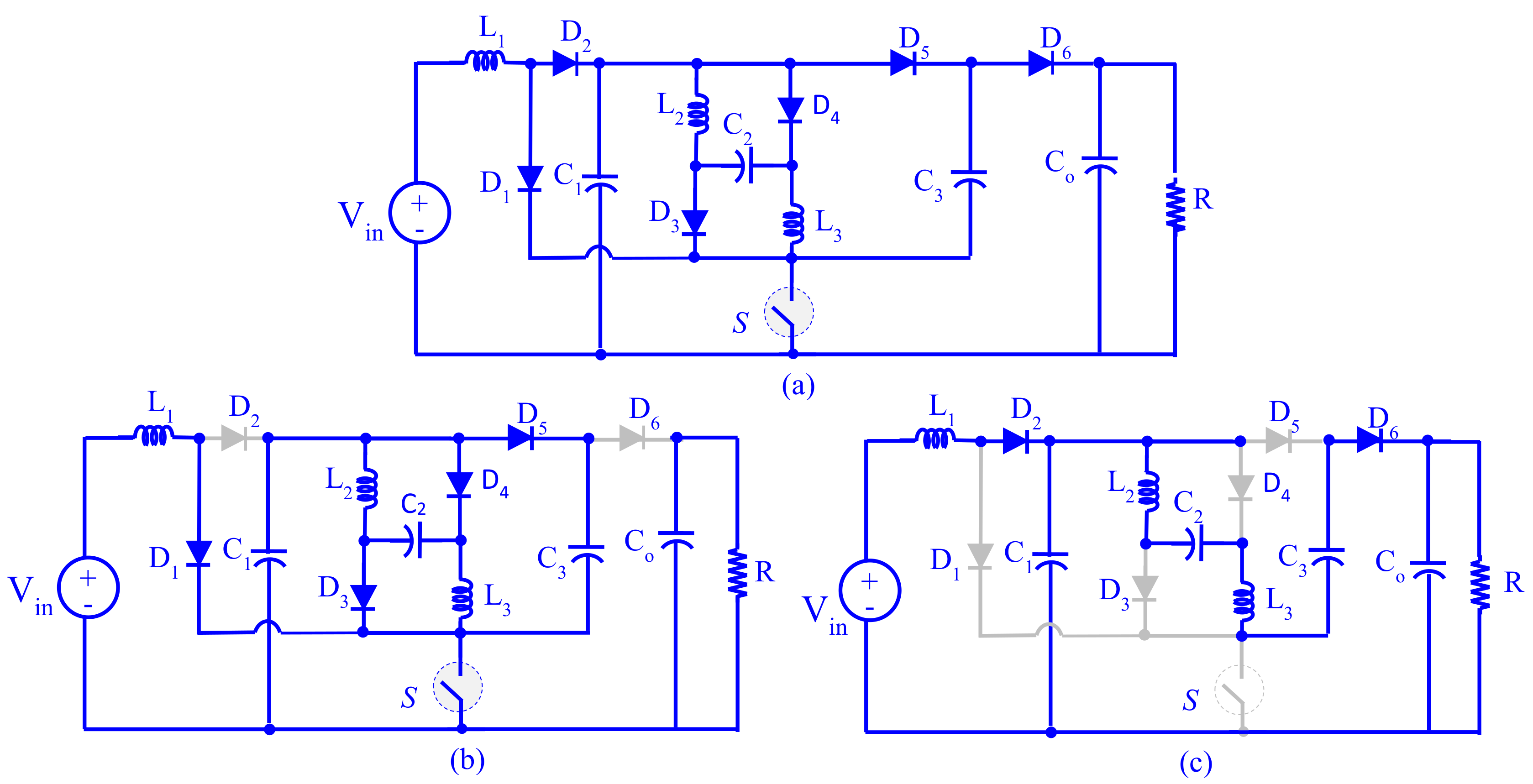
Figure 2b illustrates the complete topology of the present converter, which is implemented by cascading a CBT, POSLLC, and VMC. In other words, this topology is a modified form of CBT. Note that the VMC has been placed instead of POSLLC’s inductor. In the second step, the modified POSLLC is replaced with the second inductor of CBT (Figure 2a). Therefore, the voltage ratio of the topology increased, and the bold features of CBT remained. Notably, this converter was designed for a continuous current mode (CCM). Moreover, the extracted relations during this section are appropriate for the ideal mode.
The activation of the first switch starts the first operating mode. Due to the activation of the switch, the first, third, fourth, and fifth diodes are activated. All inductors are magnetized by their positive voltages during this operating mode. The second and third capacitors are charged as well. However, the rest of the capacitors become discharged. Notably, the first, second, and third capacitors are connected in parallel. Therefore, the first capacitor voltage is copied to the second and third capacitors. We should note that the expressing topology of the first mode is illustrated in Figure 3b. The inactivation of the switch starts the second operating mode. Consequently, the second and last diodes begin to ’conduct’. The applied voltage to the inductor becomes negative. Therefore, all of them are demagnetized. The first, second, and third capacitors are connected in series. Consequently, a higher voltage is applied to the second and third capacitors. Notably, the expressing circuit of the second mode is illustrated in Figure 3c. The voltage equations of the inductors and current relations of the capacitors are expressed as (1).
L 1 d i L 1 d t = D ( V i n ) + ( 1 D ) ( V i n v C 1 ) L 2 d i L 2 d t = D ( v C 1 ) + ( 1 D ) ( v C 1 + v C 2 v ) L 3 d i L 3 d t = D ( v C 1 ) + ( 1 D ) ( v + v C 3 v C o ) C 1 d v C 1 d t = D ( i L 2 + i L 3 + i C 2 + i C 3 ) + ( 1 D ) ( i L 1 i L 2 ) C 2 d v C 2 d t = D ( i C 2 ) + ( 1 D ) ( i L 2 ) C 3 d v C 3 d t = D ( i C 3 ) + ( 1 D ) ( i L 2 ) C O d v C O d t = D ( I O ) + ( 1 D ) ( i L 2 I O )
The average voltage of the inductor and the average current of the capacitor is zero. In other words, all of the stated equations of (1) are equal to zero. Therefore, the average capacitor voltage and the average current of the inductor can be calculated as (2).
V C 1 = V C 2 = V C 3 = V i n 1 D , V C o = 3 D ( 1 D ) 2 V i n I L 1 = 3 D ( 1 D ) 2 I o , I L 2 = I L 3 = I o 1 D , i C 2 = i C 3 = I o D
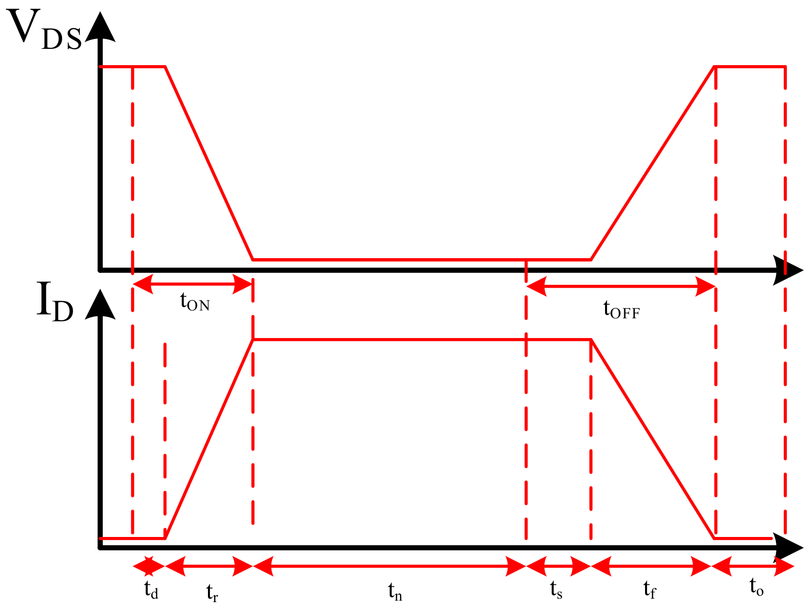
Hard-switching was selected for the proposed converter as shown in Figure 4. However, soft-switching has many advantages and its investigation will be in future research. The average crossing current of the semiconductors can be calculated by determining the average current of the inductor; the voltage stress can be determined by the average voltage capacitor as (3).
I S = 1 + 2 D D 2 ( 1 D ) 2 I o , I D 1 = D ( 3 D ) ( 1 D ) 2 I o I D 2 = 3 D 1 D I o , I D 3 = I D 4 = I o 1 D , I D 5 = I D 6 = I o V S = V D 5 = V D 6 = 2 V i n ( 1 D ) 2 , V D 1 = 1 + D ( 1 D ) 2 V i n V D 2 = V i n 1 D , V D 3 = V D 4 = V i n ( 1 D ) 2
The current ripple of the inductor and the voltage ripple of the capacitor are as in (4).
Δ i L 1 = D V i n L 1 f s , Δ i L 2 = D V i n L 2 f s ( 1 D ) Δ i L 3 = D V i n L 3 f s ( 1 D ) , Δ v C 1 = 2 D I o ( 1 D ) 2 f s C 1 Δ v C 2 = I o f s C 2 , Δ v C 3 = I o f s C 3 , Δ v C o = D I o f s C o

3. Discontinuous Current Mode

The converters operating in the continuous/discontinuous conduction modes (CCM and DCM) depend on the average current of the inductor (besides the current ripple). In other words, the current ripple increases to more than twice the average current of the inductor, concluding DCM. Therefore, the boundary value of the inductor is written as (5).
L 1 > R D ( 1 D ) 4 2 f s ( 3 D ) 2 , L 2 > R D ( 1 D ) 2 2 f s ( 3 D ) , L 3 > R D ( 1 D ) 2 2 f s ( 3 D )
The average current of the inductor is related to the average output current. Consequently, the operating region of the converter in CCM or DCM was determined according to the duty cycle and output current, see Figure 5.
CCM and DCM voltage gain relations are not the same. Considering D as the duty cycle and D1 as the ratio of the ON time of the last diode over the whole switching period, the expressing voltage gain of DCM can be expressed as (6).
V o V i n = ( D + D 1 ) ( 3 D 1 + 2 D ) D 1 2

4. Converter Behavior in the Non-Ideal Mode

Considering the equivalent series resistance of the inductors, the switch and diodes determine the actual behavior of the converter. The mentioned relation is reported in (7).
V o V i n = 3 D ( 1 D ) 2 ( 1 r L R f 1 ( D ) r S R f 2 ( D ) r D R f 3 ( D ) ) f 1 ( D ) = 3 D 2 10 D + 11 ( 1 D ) 4 , f 2 ( D ) = 3 D 3 11 D 2 + 7 D + 5 ( 1 D ) 4 f 3 ( D ) = D 2 8 D + 12 ( 1 D ) 3
The written parts of the parasitic components are equivalent series resistances of the inductors ( r L ), the dynamic resistance of the switch ( r S ), and the dynamic resistances of the diodes. The written R in (7) presents the load value. According to the reported equations in (2) and (7), 
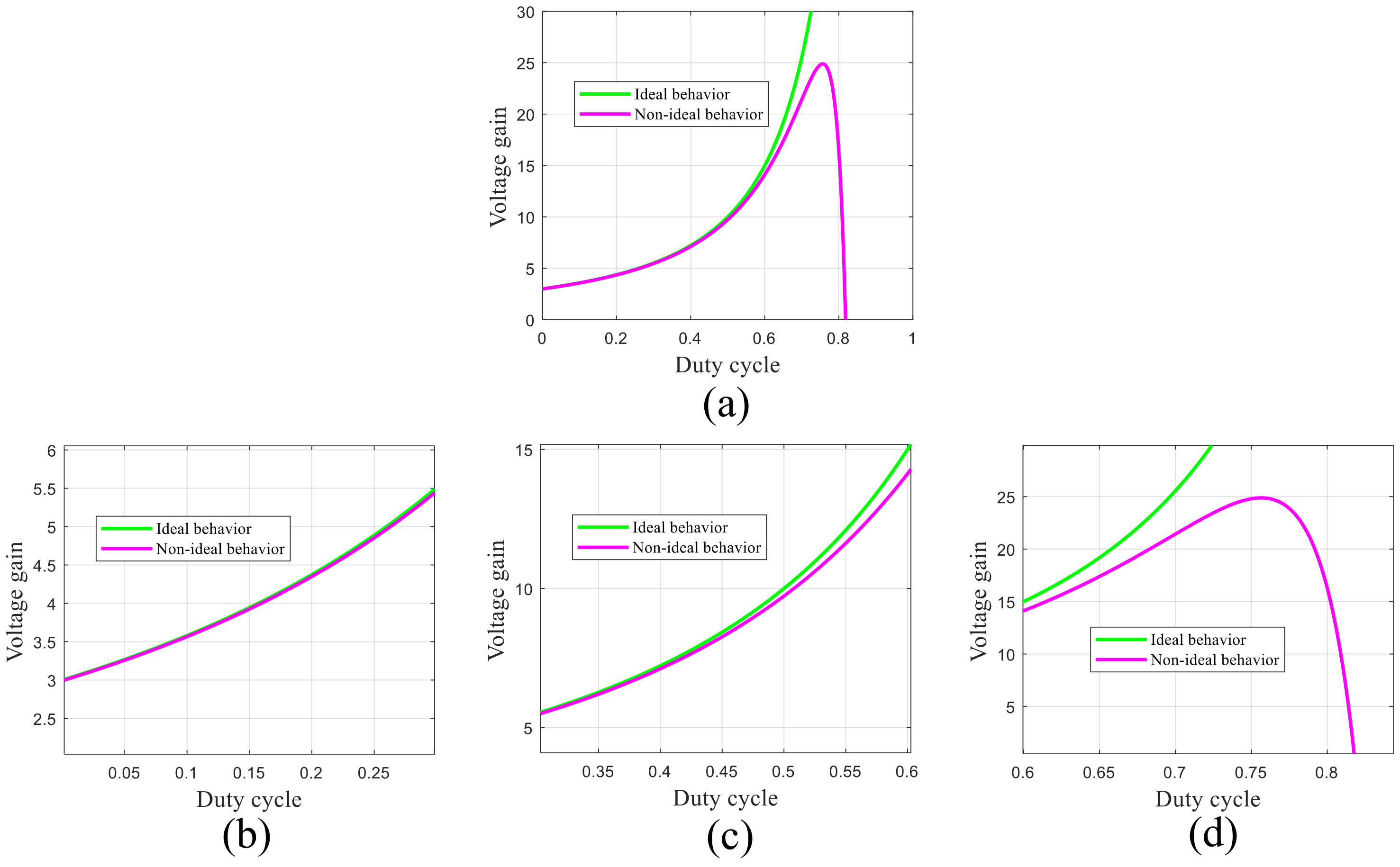
Figure 6 compares the voltage gains in both the ideal/non-ideal modes.
According to this figure, there are no differences in the behaviors of the ideal/non-ideal voltage ratios, while the duty cycle value is lower than 65%. However, the difference increases as the duty cycle approaches unity. Moreover, as the duty cycle approaches unity, the voltage ratio’s ’decreasing behavior’ appears. We should note that according to (7), the voltage ratio behavior in the non-ideal state depends on the load value. In addition, besides a constant output voltage, the decrease of the load resistance concludes and the output power increases. In 
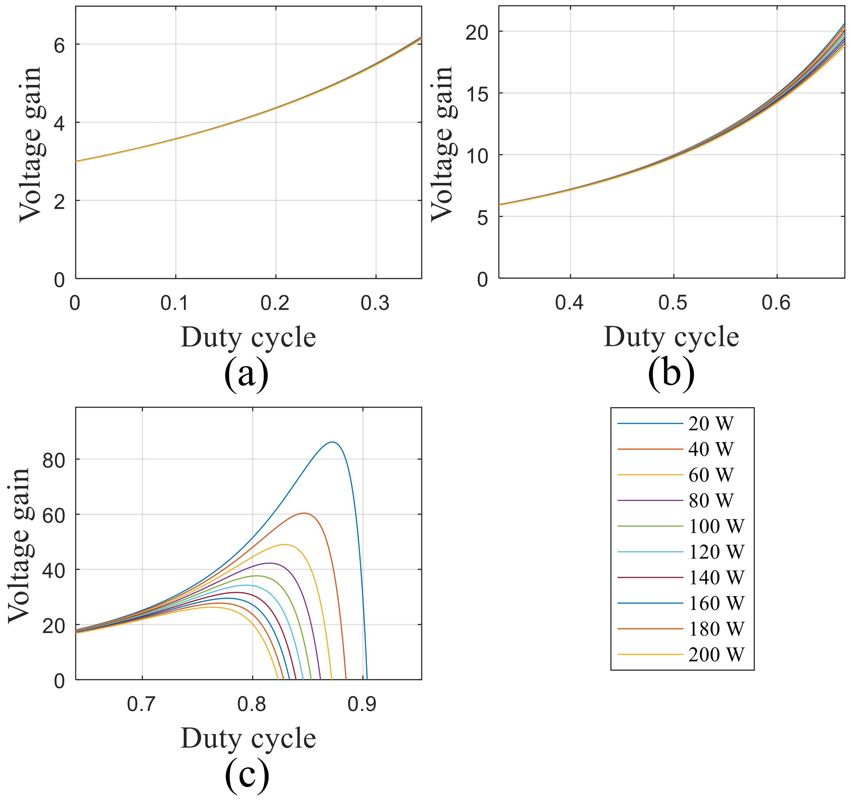
Figure 7, the voltage gain of the non-ideal state is compared to the various output powers. It can be understood that the provided voltage gains in the various output powers are the same, while the duty cycle is lower than 60%. However, the difference between the mentioned plots increases as the duty cycle becomes closer to unity. Moreover, its maximum value and corresponding duty cycle decrease. Therefore, the output power increase decreases the corresponding interval of the voltage gain’s rising behavior.
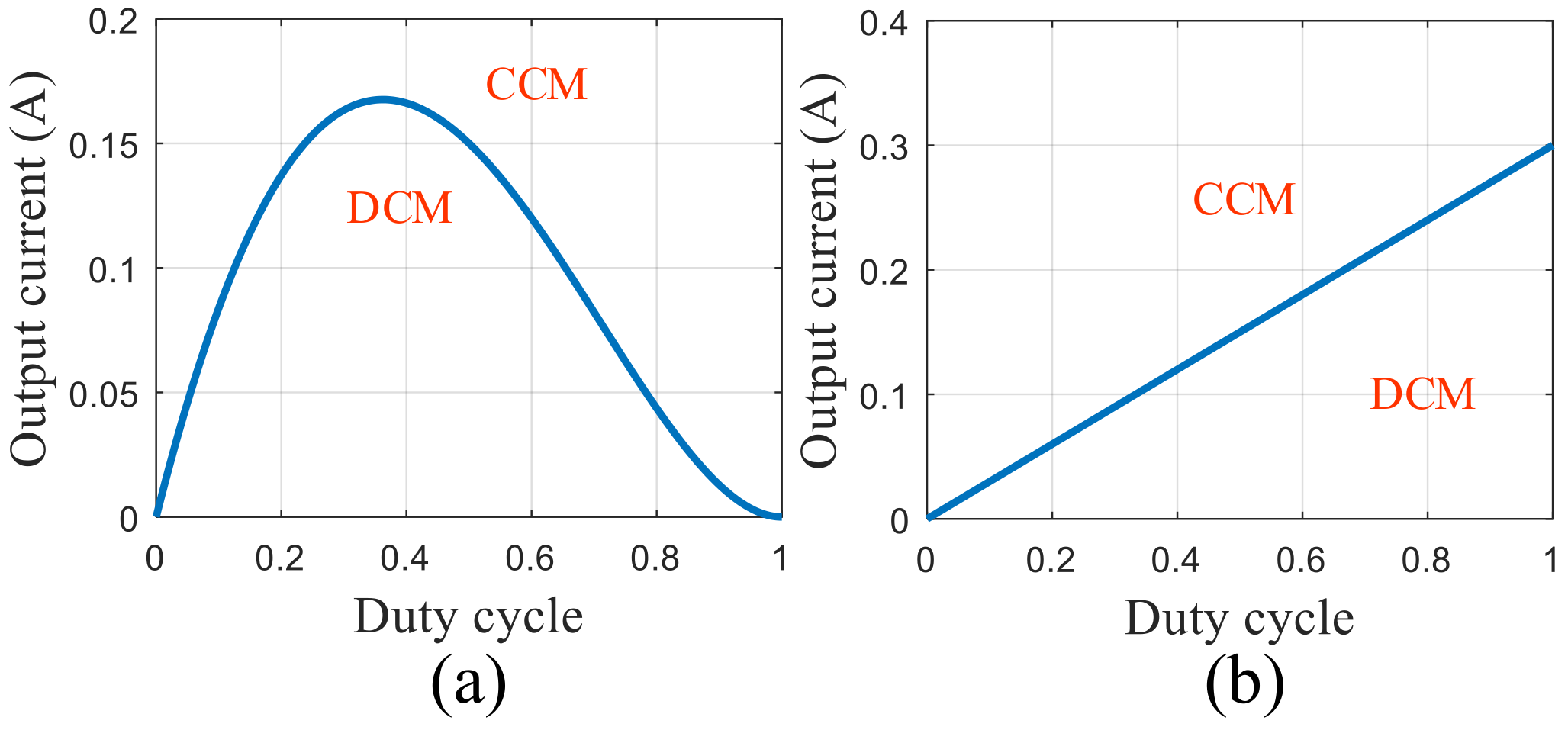
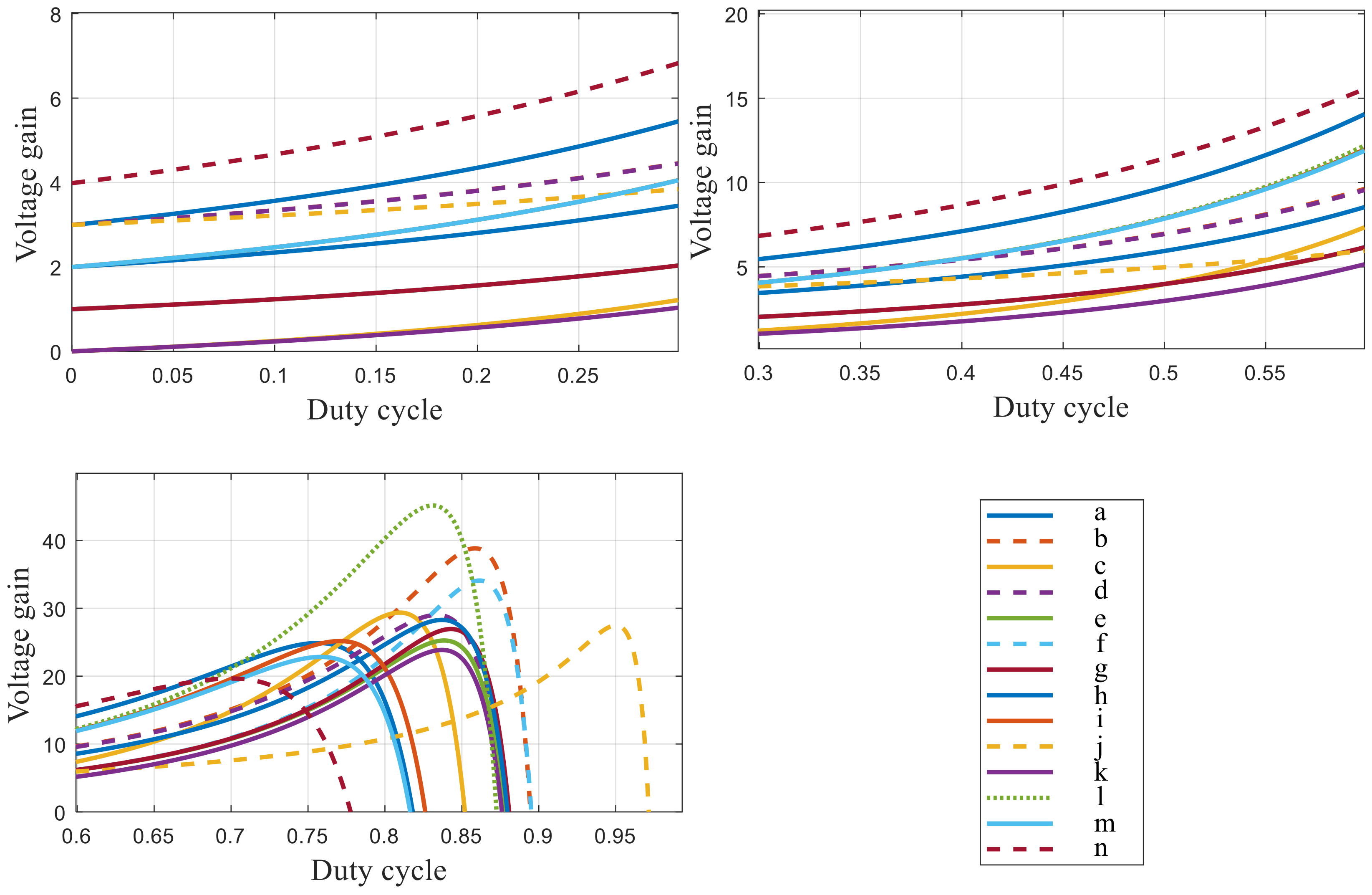
According to Figure 8, the provided voltage gains by the proposed converter and introduced topology in [30] are higher than the rest. In other words, the provided voltage gains by varying the duty cycle from 0 to 72% cover from 3 to 20-times. Notably, the achieved voltage gains in the higher duty cycle percentages are useless. In other words, the provided voltage gain in the mentioned region has poor efficiency. Therefore, the voltage gains of the higher percentages are not recommended. Moreover, the proposed converter and [30] show their better functions in the lower duty cycle percentages than the rest.
The efficiency of this converter was modeled considering the inductor conduction loss, MOSFET conduction and frequency loss, and diode conduction loss, besides neglecting the hysteresis and eddy current losses of the inductors and frequency losses of the diodes. The mentioned types of losses have been formulated (8).
P L = r L 1 ( 3 D ) 2 ( 1 D ) 4 + ( r L 2 + r L 3 ) 1 ( 1 D ) 2 P o R P S C = ( 1 + 2 D D 2 ) 2 D ( 1 D ) 4 , P S S = 1 + 2 D D 2 ( 1 D ) 4 V i n I o f s t O F F P D = ( D ( 3 D ) ( 1 D ) 2 V D F 1 + 3 D 1 D V D F 2 + V D F 3 + V D F 4 1 D . . . + V D F 5 + V D F 6 ) η = P o P o + P L + P S C + P S S + P D
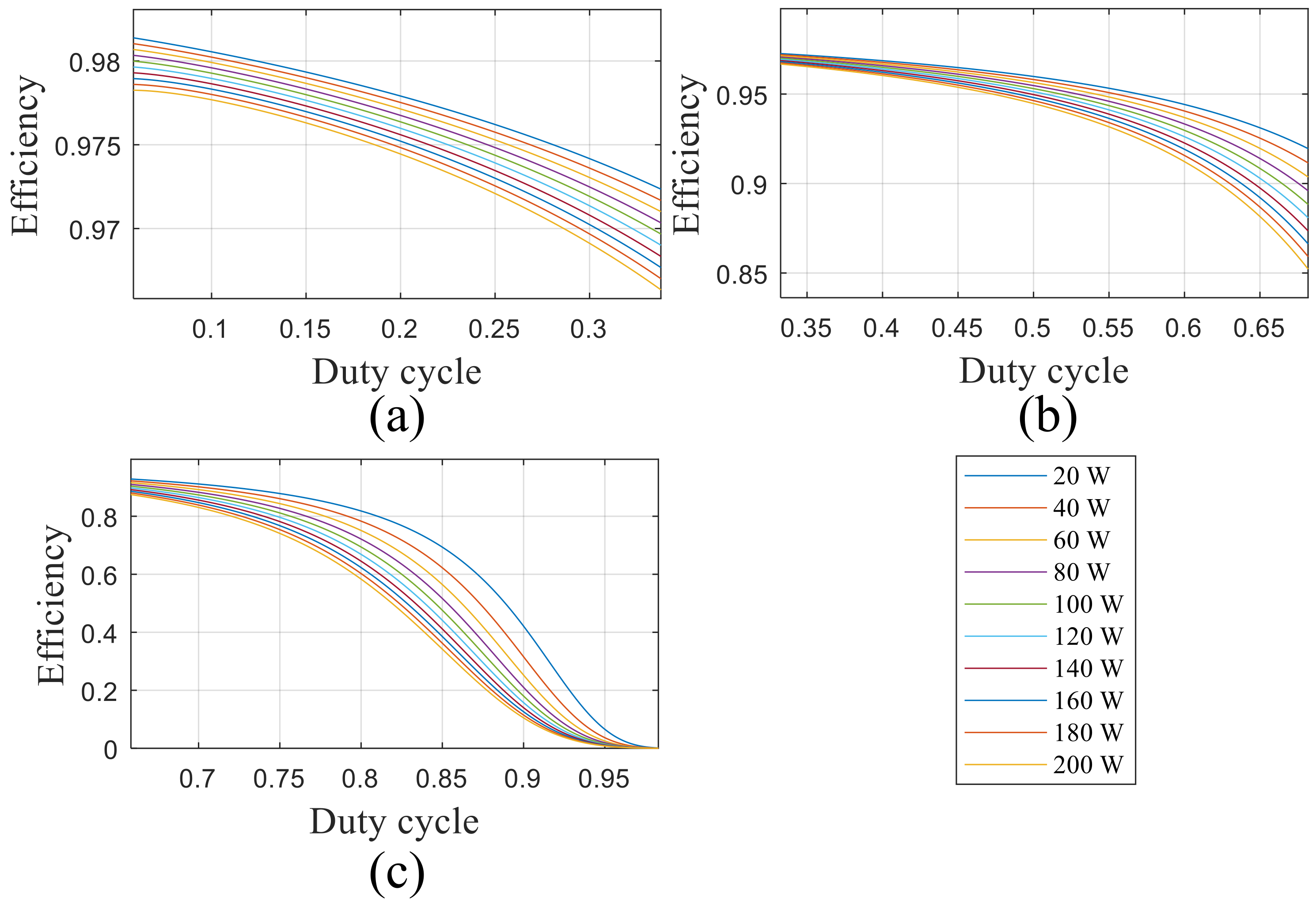
Figure 9 presents the efficiency behavior and the varying output power. Notably, Figure 9a,b show the duty cycle percentages varying from 0% to 62%, concluding the converter’s efficiency (higher than 90%). Moreover, as the duty cycle increases from 62% to 69%, the converter’s efficiency becomes lower than 90% and higher than 80% for the output powers of 20 to 100 W. We should note that the increase in the duty cycle to more than 80% concludes the efficiency (lower than 80%) for all of the mentioned output powers.
Table 1 summarizes the comparisons between the topologies and features of the converters in [18,19,20,21,22,23,24,25,26,27,28,29,30] and the proposed converter. All topologies in [18,19,20] have two switches, three diodes, two inductors, and three capacitors. The proposed converters in [21,22,23] have two inductors, capacitors, switches, and diodes. The rest of the converters only have one switch. Topologies in [24,25,28,29] have five diodes, and the ones in [26,27] have four and three diodes, respectively. The converter in [30] and this paper have three inductors. Two inductors are used in [18,19,20,21,22,23,24,25,26,27,28] topologies and the rest have three inductors. The number of capacitors in [18,19,20,26,29] is three. In [24,25,28,30], four capacitors are used and the remaining topologies use just two capacitors. The topologies in [21,27] have discontinuous input currents. The input current ripples in [18,20,26,28,29,30] are not insignificant. Notably, the topologies of [19,22,23,24,25], and the proposed one eliminate the input current ripple via the presence of the inductor at the input of the converter. Finally, the topologies of [19,27] have no common ground between the input source and the load.
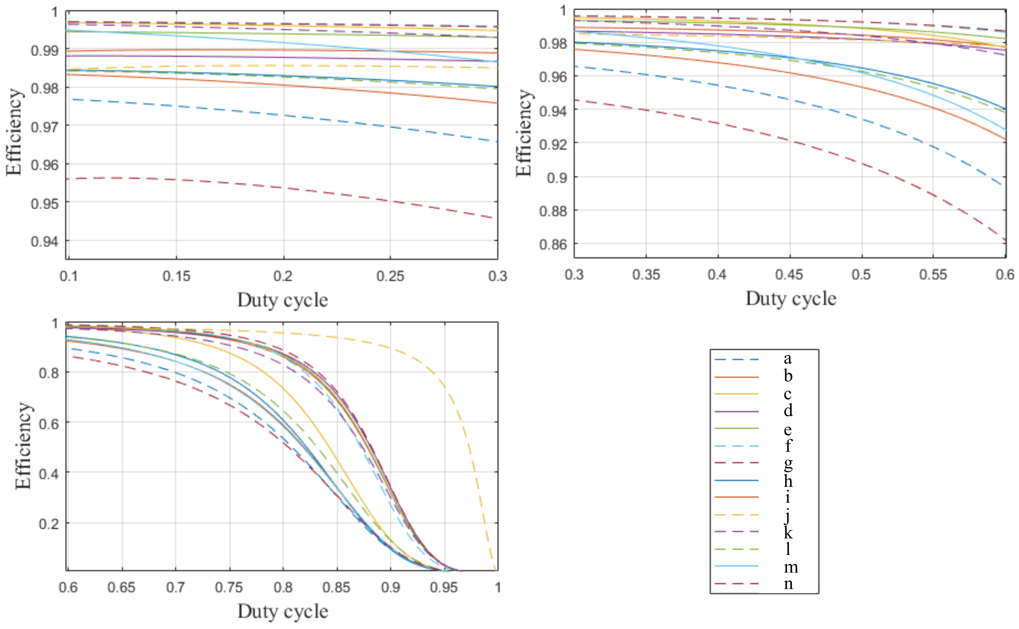
Figure 10 compares the efficiency in the same output power among the proposed topology in this paper and [18,19,20,21,22,23,24,25,26,27,28,29,30]. While the duty cycle varies from 0 to 30%, all topologies provide efficiency higher than 94%. Increasing the duty cycle from 30% to 60% decreases the efficiency of [30] from 94% to 86%. However, the provided efficiency by the rest is higher than 90% in the mentioned duty cycle interval. The duty cycle varying from 60 to 70% concludes the efficiency value between 80 and 90%. However, the rest keep their higher values until there are higher duty cycle percentages. The proposed converter provides high-voltage gain and efficiency values through lower duty cycle percentages.
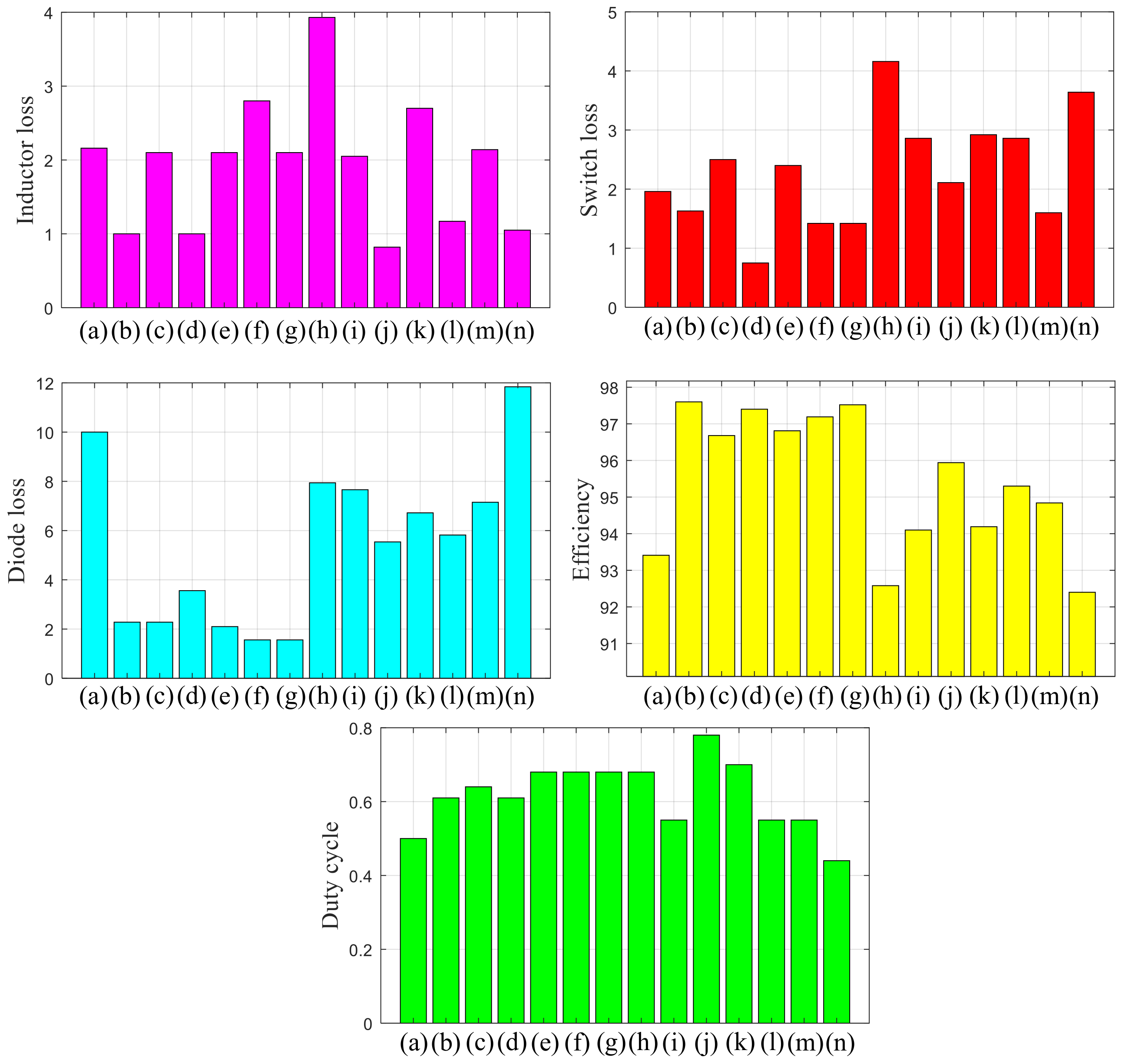
Figure 11 compares the inductor, switch, and diode losses beside the efficiency and duty cycle percentage. This comparison was conducted using a 200 W output power and a duty cycle that produced a 10-times voltage gain. The suggested topology inductor losses were less than the converters in [22,24,27]. Moreover, these losses were approximately the same as in [19,21,23,25,29]. Additionally, the suggested converter had a lower switch loss than the switches in [19,21,24,25,26,27,28,30]. In the diode losses, only the recommended topology of [30] had lower diode losses than the proposed converter. The higher losses were due to the six diodes in this converter. According to Figure 11d, the efficiency of the proposed converter is higher than in [24,30]. Note that the difference in the efficiency values is less than 4%. Figure 11e shows that the required voltage gain for the proposed converter is less than the gains in [18,19,20,21,22,23,24,25,26,27,28,29].
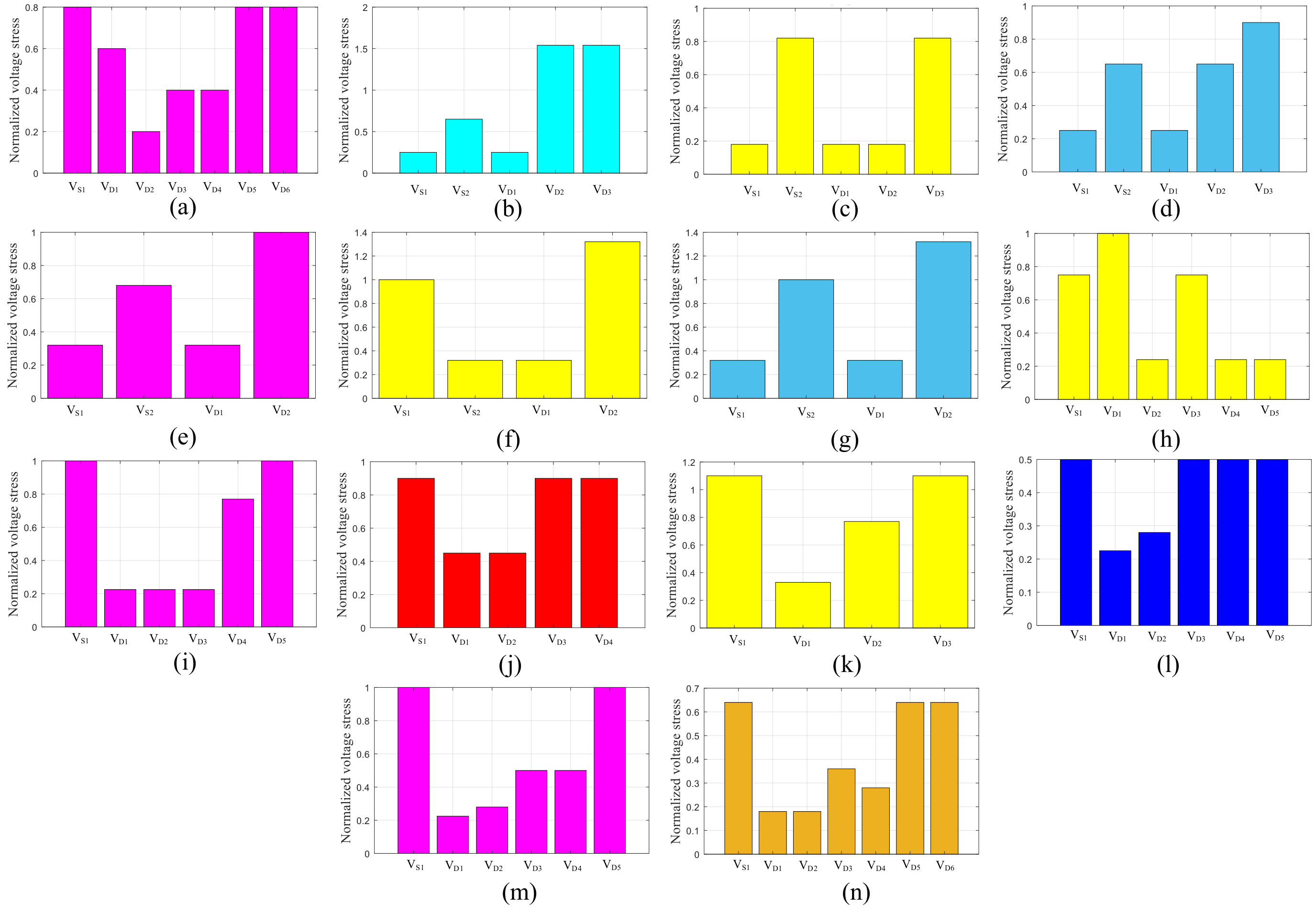
Figure 12 presents the normalized voltage stress of the proposed converter as well as [18,19,20,21,22,23,24,25,26,27,28,29,30]. According to this figure, all stresses are smaller than unity. However, some of the voltage stresses in [18,21,22,23,24,25,27,29] are equal to or greater than unity. 
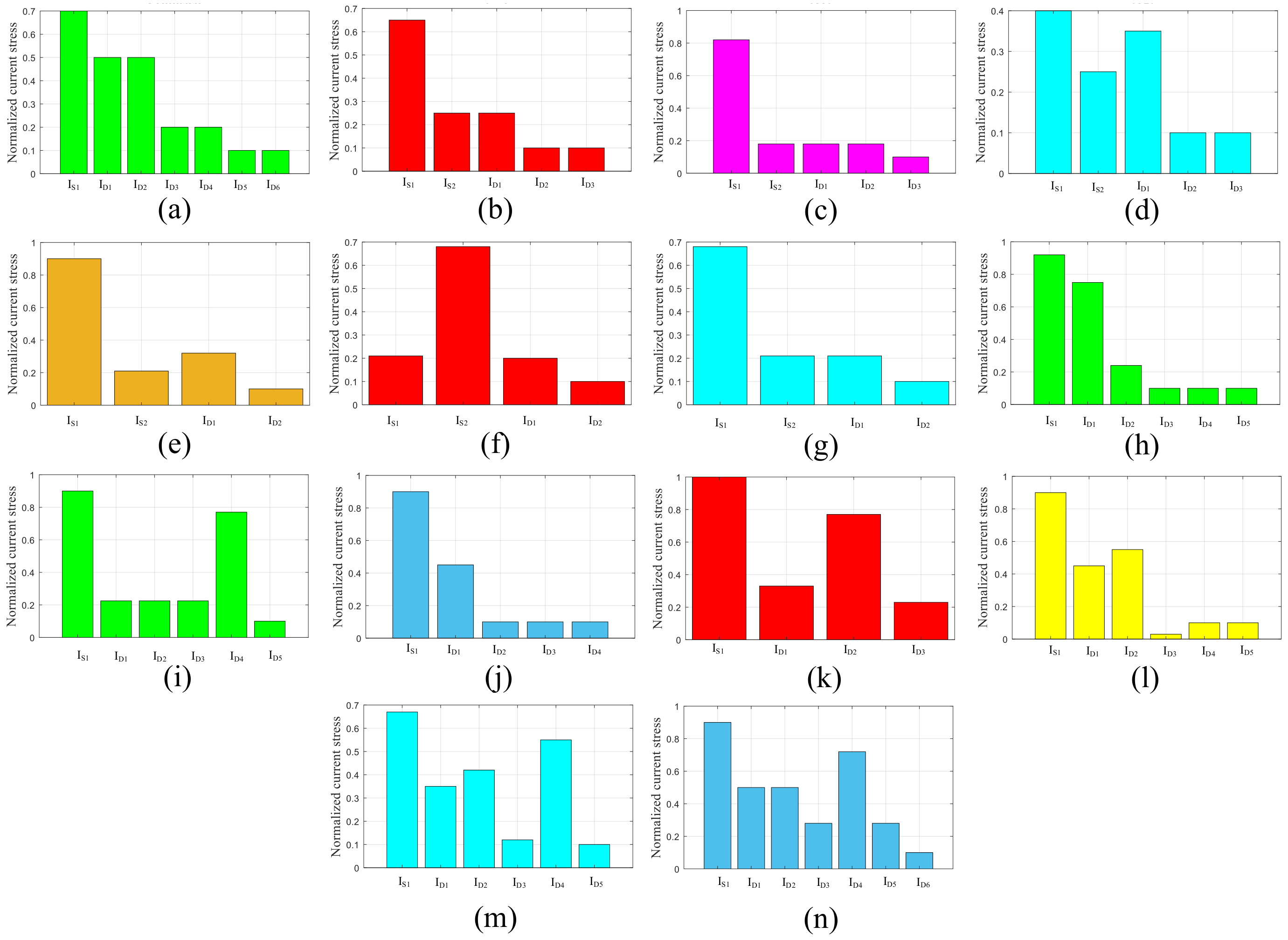
Figure 13 shows the semiconductor’s normalized current stress of 0.7. However, in [19,21,24,25,26,27,28], the stresses are more than 0.7. In the suggested converter, each diode current stress is less than 0.5. However, several of the diode stresses in [24,25,27,28,29,30] are more than 0.5.

5. Simulation and Experimental Results

This section presents the simulation and experimental results to validate the theoretical analysis. PLECS software tools were used to simulate the proposed converter. Such software is suitable for power electronics and control projects. Simulation results were obtained using realistic assumptions. Moreover, the energy-storing components had to be determined using functional constraints, such as input voltage, the duty cycle, the output current, the current ripple of inductors, and the voltage ripple of capacitors. The input voltage was 20 V, which was defined by the equipment limits. In addition, the switching frequency of MOSFET was 50 kHz due to the frequency limits of employing the wires of the inductors. Moreover, the power quality considerations defined 30% and 5% as the current ripple of the inductor and the voltage ripple of the capacitor, respectively. As mentioned before, the duty cycle was 50%, with an equal energy-storing/releasing time and provided suitable operating conditions; moreover, (9) expresses the average current of the inductor and average voltage of the capacitor.
V C 1 = V C 2 = V C 3 = 40 V , V C o = 200 V I L 1 = 10 A , I L 2 = I L 3 = 2 A
Using the calculated average voltages/currents (besides the specified current/voltage ripples) gives the following inductors and capacitors in (10).
L 1 = 66.6 μ H , L 2 = L 3 = 666.6 μ H C 1 = 40 μ F , C 2 = C 3 = 10 μ F , C o = 1 μ F
Using the parameters in (10) gave the simulation results in Figure 14 and Figure 15. 
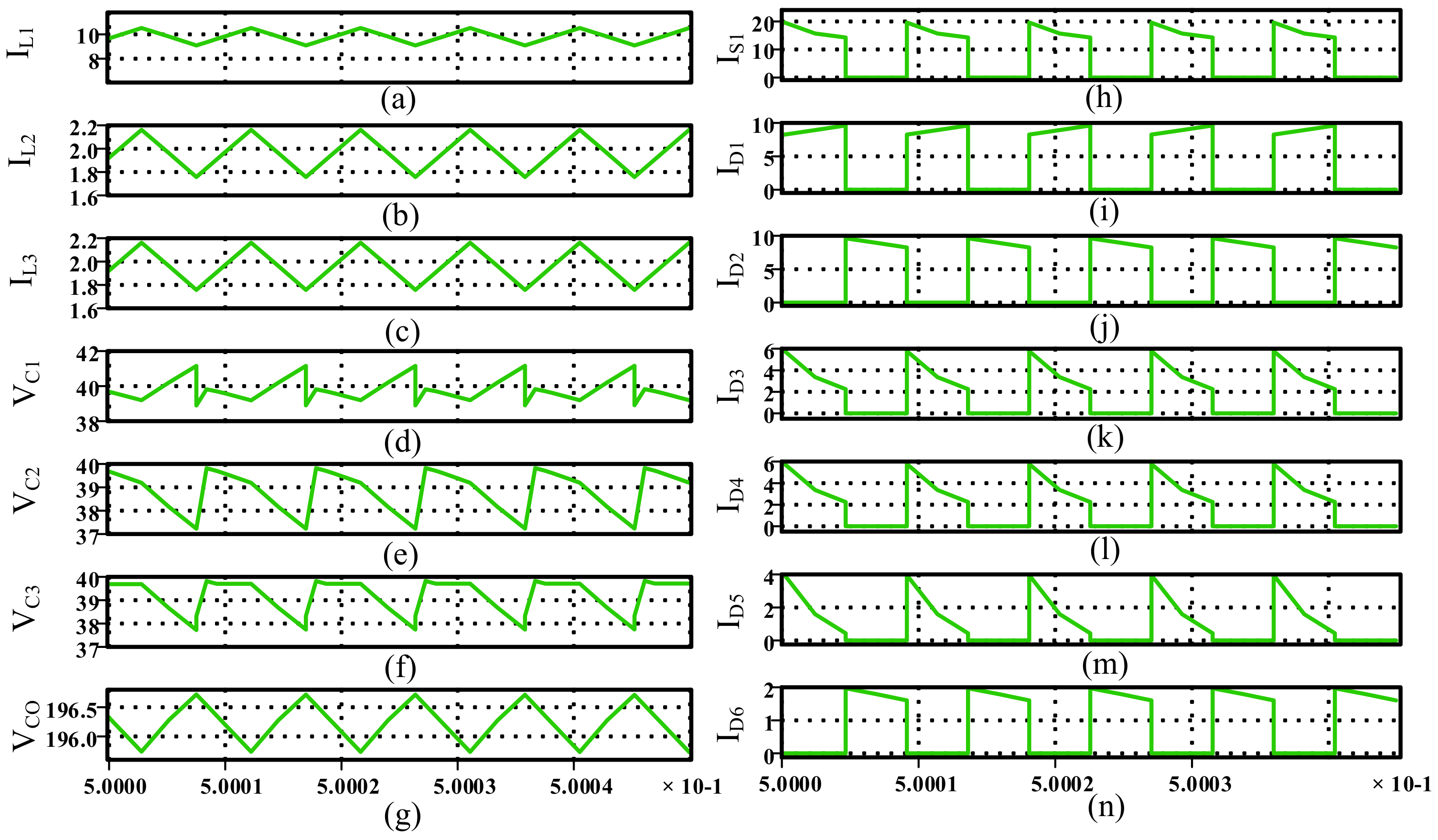
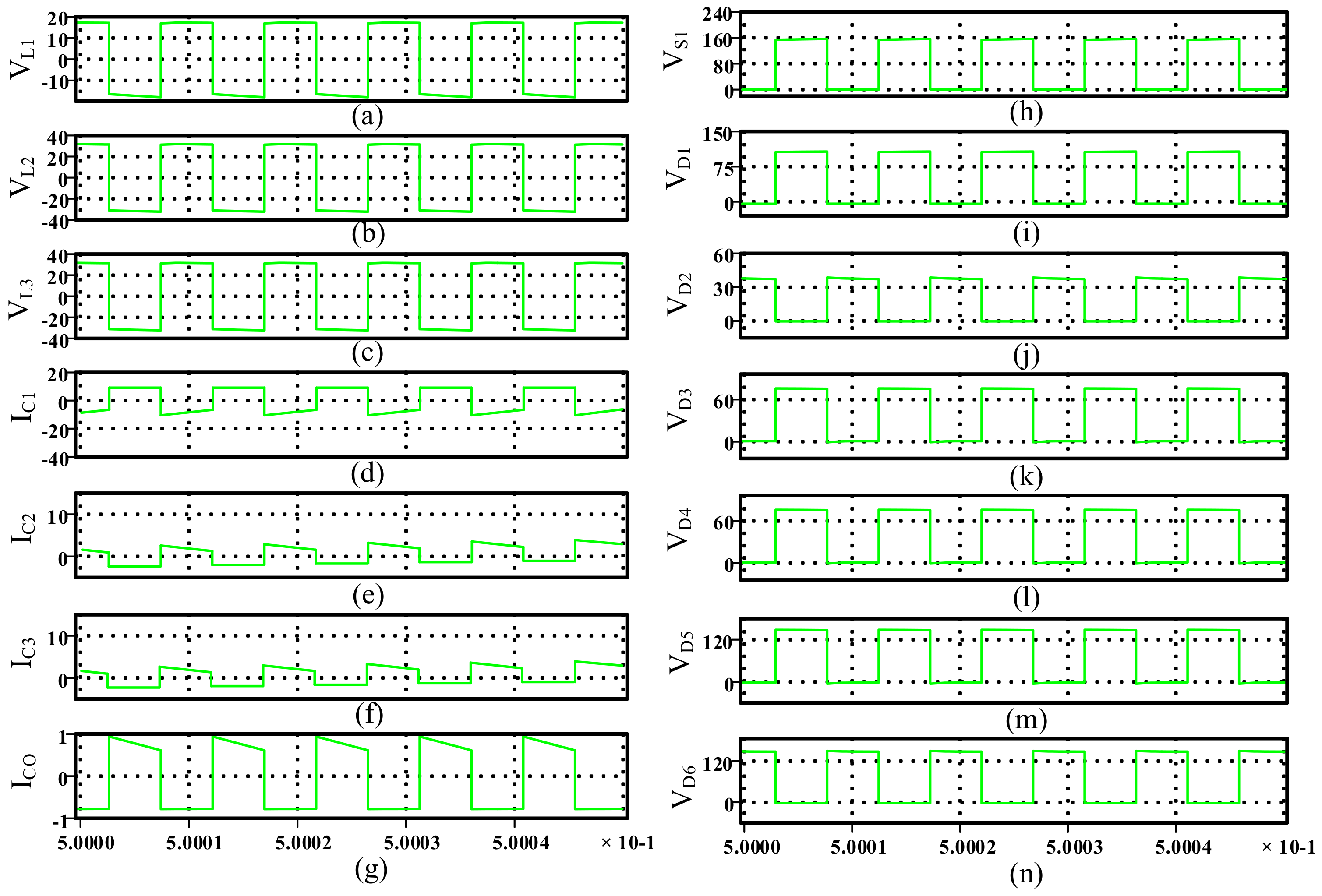
Figure 14 depicts the inductor current, the capacitor voltage, and the semiconductor current waveforms. Additionally, Figure 15 shows the inductor voltage, the capacitor current, and the semiconductor voltage. According to the inductor current and capacitor voltage waveforms, their average values are as in (11).
V C 1 = 40 V , V C 2 = 38.5 V , V C 3 = 39 V , V C o = 196 V I L 1 = 10 A , I L 2 = I L 3 = 2 A
The comparisons of the corresponding values of (11) and (9) defined their compatibilities and validated the correctness of the extracted relations. The differences in the average voltage of the capacitors refer to the voltage drops of the diodes.
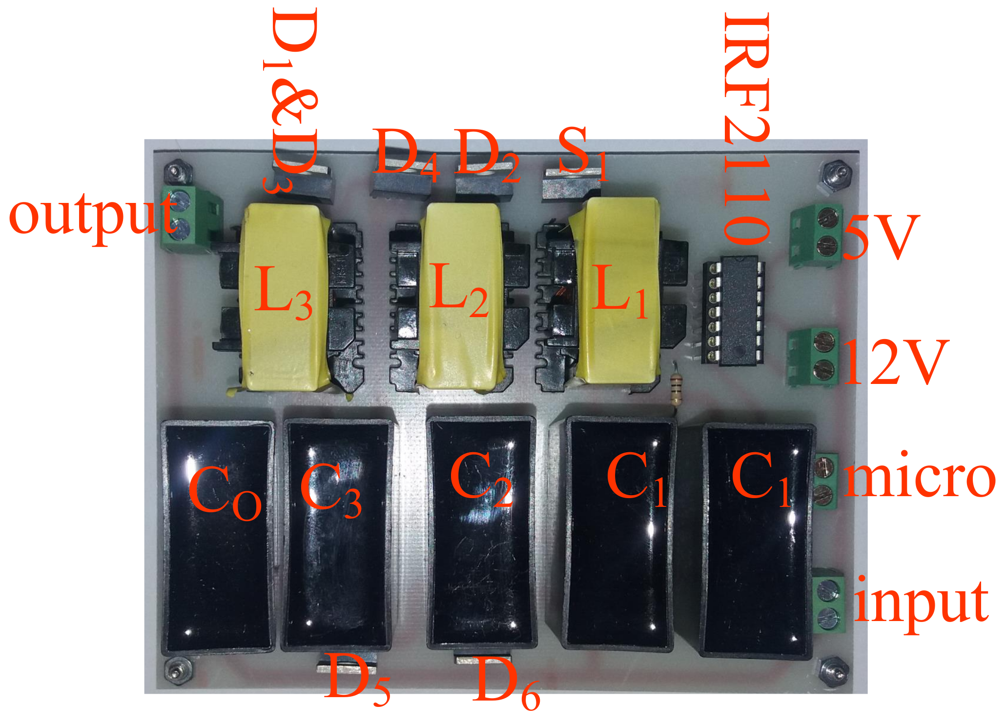
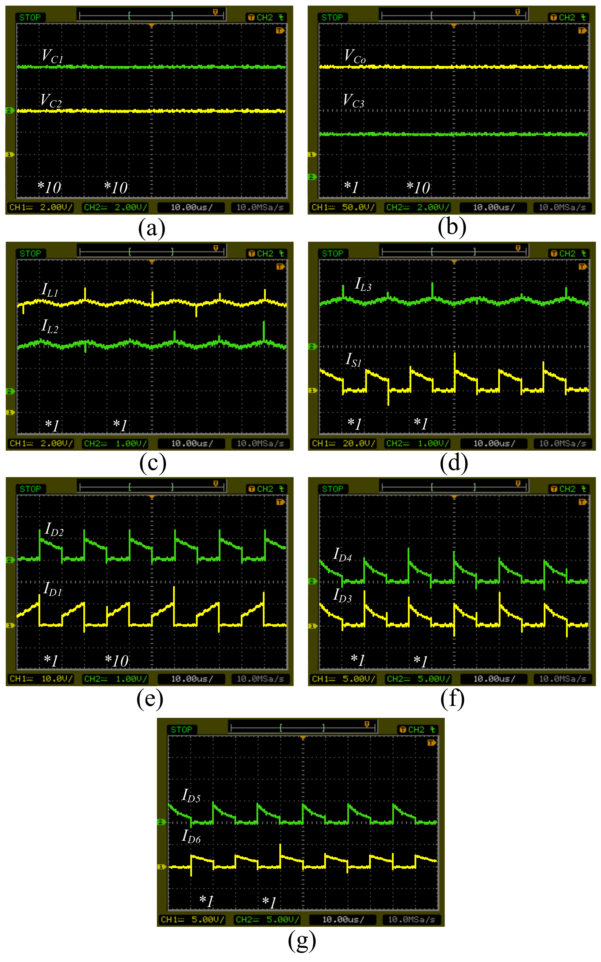
A 200 W prototype of the proposed converter was built and it is illustrated in Figure 16. The components’ voltage/currents are shown in
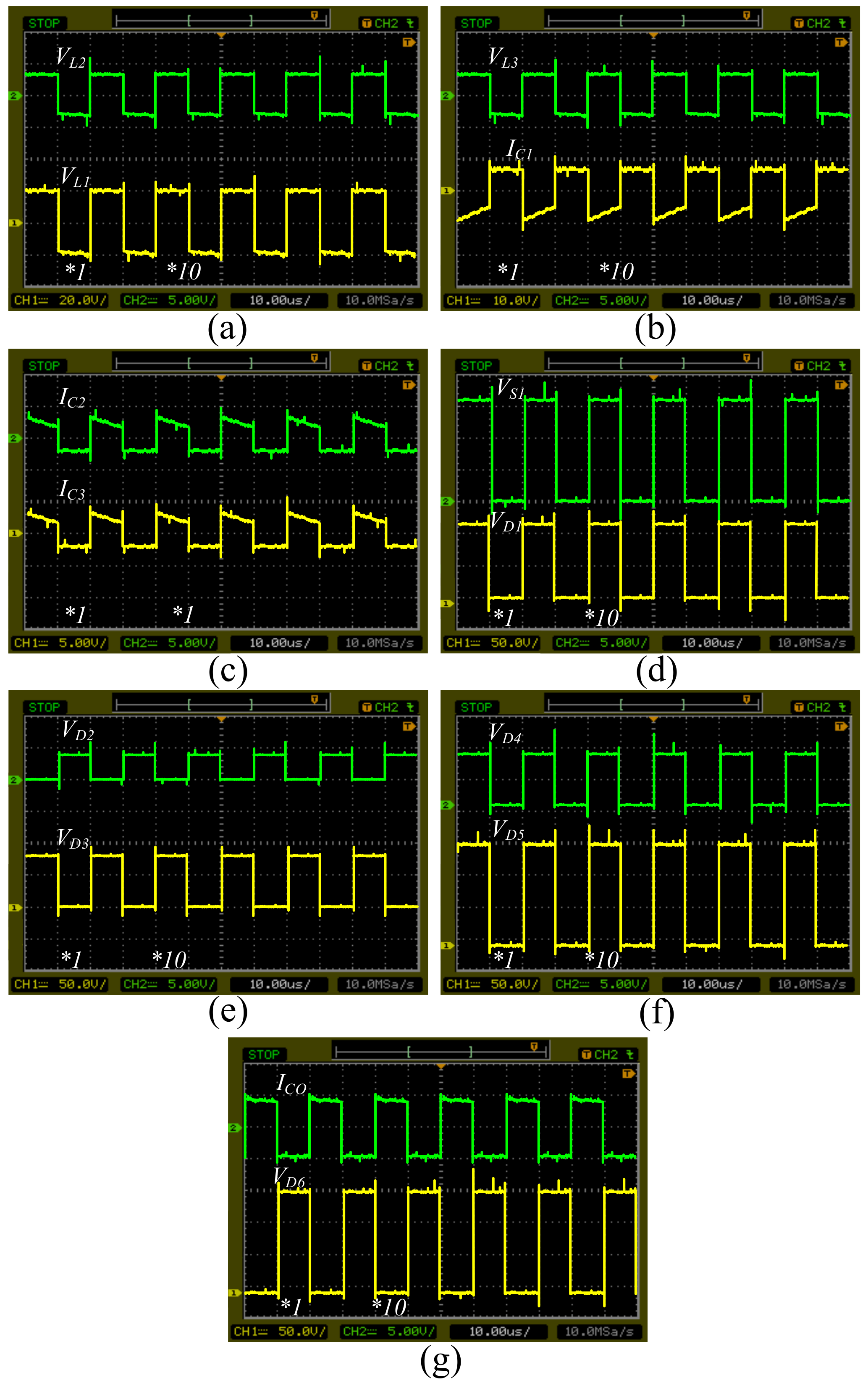
 Figure 17 and Figure 18, which present the experimental results. Figure 16 shows the current waveforms of the inductors and semiconductors, besides the capacitor’s voltage waveforms. Figure 17 shows the inductor voltage, the capacitor current, and the semiconductor voltage waveform. From Figure 17 and Figure 18, the average current and voltage of inductors are given by (12).
V C 1 = 38 V , V C 2 = 37 V , V C 3 = 36 V , V C o = 190 V I L 1 = 9.4 A , I L 2 = I L 3 = 1.9 A
Comparing the experimental results with the simulation results and primary design considerations, we can see the expected difference. This discrepancy relates to the voltage drop in the prototype’s diodes. Therefore, the voltage values are lower than the simulation results and design considerations. According to Figure 17, the average voltage of the inductors and the average current of the capacitors are zero, as assumed. Moreover, (13) gives the semiconductor current/voltage stresses according to Figure 17 and Figure 18, respectively.
I S 1 = 6.3 A , I D 1 = 4.5 A , I D 2 = 4.5 A , I D 3 = 1.8 A I D 4 = 1.8 A , I D 5 = 0.9 A , I D 6 = 0.9 A V S 1 = 154 V , V D 1 = 116 V , V D 2 = 38 V , V D 3 = 80 V V D 4 = 80 V , V D 5 = 154 V , V D 6 = 154 V
According to the theoretical relations of the voltage/current stresses, the mentioned values are as in (14).
I S 1 = 6.65 A , I D 1 = 4.75 A , I D 2 = 4.75 A , I D 3 = 1.9 A I D 4 = 1.9 A , I D 5 = 0.95 A , I D 6 = 0.95 A V S 1 = 160 V , V D 1 = 120 V , V D 2 = 40 V , V D 3 = 80 V V D 4 = 80 V , V D 5 = 160 V , V D 6 = 160 V
Based on the simulation results, the voltage/current stresses of the semiconductors are as in (15).
I S 1 = 7 A , I D 1 = 5 A , I D 2 = 5 A , I D 3 = 2 A I D 4 = 2 A , I D 5 = 1 A , I D 6 = 1 A V S 1 = 157 V , V D 1 = 117 V , V D 2 = 40 V , V D 3 = 78 V V D 4 = 78 V , V D 5 = 157 V , V D 6 = 157 V
The differences in the reported values stand from the average voltage in the capacitor prototype. Therefore, there is a difference in the semiconductor voltage compared to the theoretical values and simulation results. Moreover, the output voltage difference causes the contrast of the average output current. Therefore, the average currents of the inductors and semiconductors are different from the simulation/theoretical outcomes. In other words, there is a negligible difference.
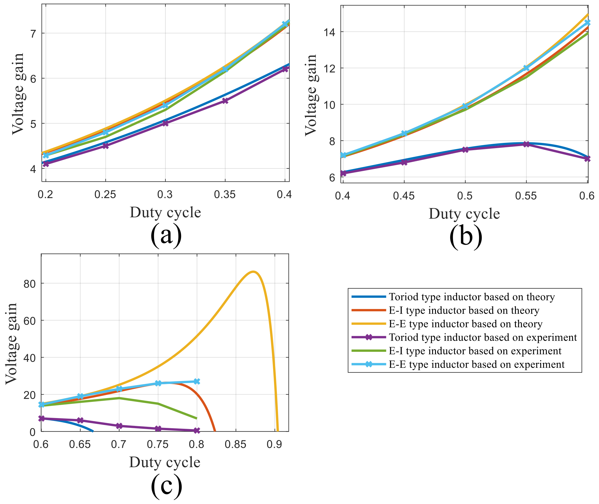
Notably, the proposed converter’s voltage gain was extracted based on the theoretical relation and experimental results for three different types of inductors. As can be understood from Figure 19, the E–E type, E–I type, and toroid type of the inductor were used. According to Figure 18, the E–E type of the inductor has better behavior regarding the voltage gain. In other words, due to the use of a low wire in the E–E type, the ESR of the inductor is low. Consequently, the corresponding figures of the E–E type have rising behaviors of wider spans. The differences in the corresponding figures regard the theoretical relations and the experimental results considering approximations. Therefore, the higher duty cycle makes the mentioned differences appear. In 
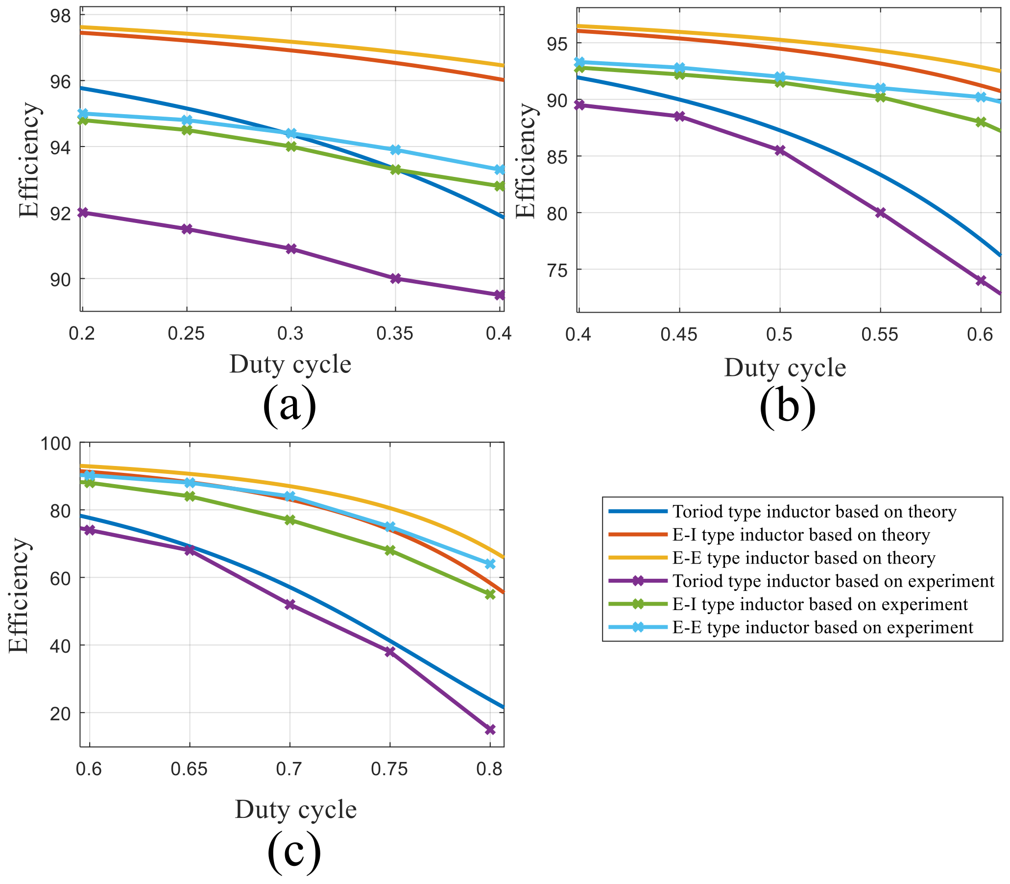
Figure 20, the converter’s efficiency based on the theoretical equations and the experimental outcomes were extracted for the E–E, E–I, and toroid types. We should note that the E–E type of inductor requires a lower wire value to achieve inductance than the rest. Therefore, the corresponding efficiency of the E–E type provides the highest value in the theoretical/experimental outcomes. The toroid type needs the highest value of the wire to achieve the same inductance. Therefore, the lowest value of the efficiency belongs to the toroid type. It is worth noting that the differences in the corresponding figures of the theoretical and experimental results were caused by neglecting some type of loss in the theoretical relation. Such an analysis was done for switches, and the results are illustrated in 
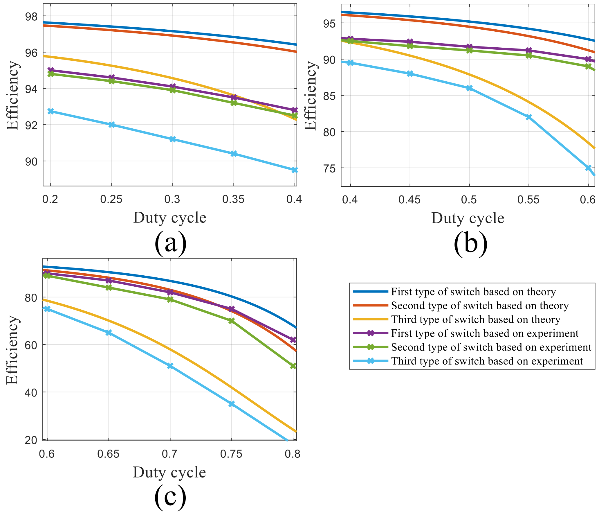
Figure 21. IRF540, IRF630, and VMK16N70OC2 are considered the first, second, and third types of switches. In Figure 21, the highest value of the efficiency (in both theory and experiment) belongs to IRF540. The dynamic resistance of the mentioned switch is lower than the rest. In addition, the VMK16N70C2, due to its high capabilities, has the highest dynamic resistance. According to the mentioned figure, IRF540 has a better function than the others. Finally, in 
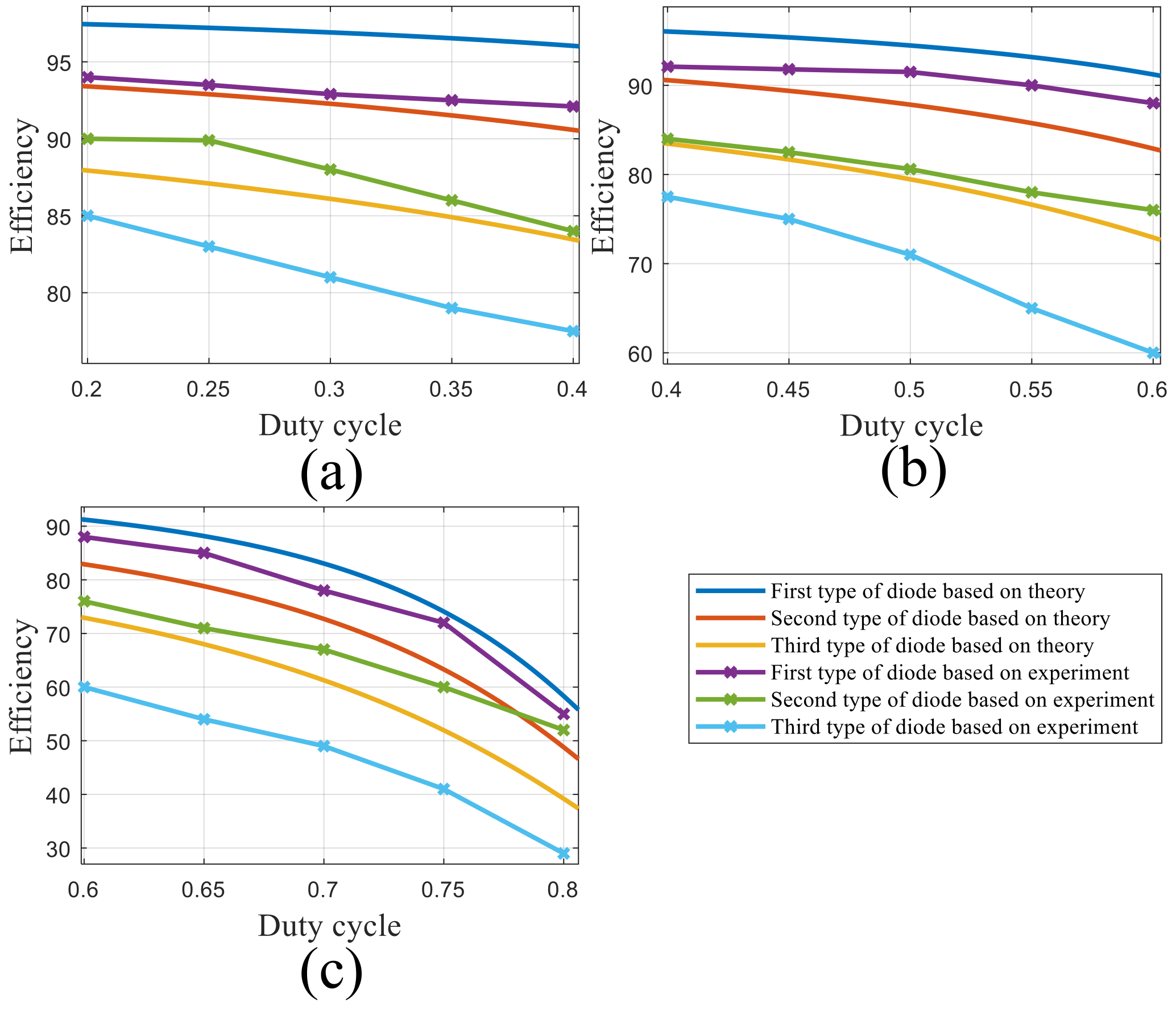
Figure 22, the converter’s efficiency was extracted for three different types of diodes. The first, second, and third diodes belong to MBRB1045G, 2015OCT, and FES8GT, respectively. In the mentioned figure, the corresponding figure of the first type obtained the highest value compared to the rest in both theory and experimental results. The last three figures explain the efficiency sensitivities according to the circuit element changes; it can be deduced that the diodes have significant effects due to their highest numbers in the proposed topology.

6. Conclusions

This paper introduced an ultra-high step-up DC–DC converter with a continuous input current. This converter’s architecture consists of a novel combination of VMC, POSLLC, and QBC topologies. When the duty cycle is at 50%, the converter attains a voltage gain of ten. The constant input current of the topology reduces the current stress on the input filter capacitor. This converter’s topology was investigated and studied under various operating conditions: ideal and non-ideal modes, as well as continuous and discontinuous current modes (CCM/DCM). The theoretical study of the proposed topology was studied for both CCM and DCM. The converter’s behavior was discussed for both the ideal and the non-ideal states of the circuit components. The proper functionality of the non-ideal case was discussed and compared with the recently suggested converter topologies. The mathematical derivation was further substantiated by a comparison of the theoretical non-ideal voltage gain relation with the experimental findings. Additionally, the efficiency of the converter was theoretically and experimentally compared to that of previously suggested converter topologies. Finally, a 200 W prototype was constructed using 20 V input voltage, 50 kHz switching frequency, 1 A output current, and operating at a 50% duty cycle. The inductors’ average current, capacitor average voltage, semiconductor average current, and semiconductor voltage were measured and compared with the theoretical results. Additionally, sensitivity analyses for the voltages were performed; it was determined that they were consistent with the derived relations. The extracted efficiency of the prototype was around 92%, which could be improved with better circuit components.

Author Contributions

Conceptualization, H.G. and L.B.-B.; methodology, H.G.; software, H.G.; validation, H.G., L.B.-B.; formal analysis, H.G.; investigation, H.G.; resources, H.G.; writing—original draft preparation, H.G., L.B.-B.; writing—review and editing, H.G., L.B.-B.; visualization, H.G.; supervision, L.B.-B.; project administration, L.B.-B.; funding acquisition, L.B.-B. All authors have read and agreed to the published version of the manuscript.

Funding

This research received no external funding.

Conflicts of Interest

The authors declare no conflict of interest.

References

  1. Maroti, P.K.; Al-Ammari, R.; Iqbal, A.; Ben-Brahim, L.; Padmanaban, S.; Abu-Rub, H. A Novel High Gain Configurations of Modified SEPIC Converter for Renewable Energy Applications. In Proceedings of the 2019 IEEE 28th International Symposium on Industrial Electronics (ISIE), Vancouver, BC, Canada, 12–14 June 2019; pp. 2503–2508. [Google Scholar]
  2. Bhaskar, M.S.; Ben-Brahim, L.; Iqbal, A.; Padmanaban, S.; Meraj, M.; Rahman, S. Hardware Implementation of a New Single Input Double Output L-L Converter for High Voltage Auxiliary Loads in Fuel-cell Vehicles. In Proceedings of the 2019 IEEE Applied Power Electronics Conference and Exposition (APEC), Anaheim, CA, USA, 17–21 March 2019; pp. 1595–1600. [Google Scholar]
  3. Hussein, B.; Alsalemi, A.; Ben-Brahim, L. High-Gain Non-isolated Single-Switch DC-DC Converters in Power Factor Correction Rectifiers: A Performance Assessment. In Proceedings of the 2022 3rd International Conference on Smart Grid and Renewable Energy (SGRE), Doha, Qatar, 20–22 March 2022; pp. 1–6. [Google Scholar]
  4. Lotfi Nejad, M.; Poorali, B.; Adib, E.; Motie Birjandi, A.A. New cascade boost converter with reduced losses. IET Power Electron. 2016, 9, 1213–1219. [Google Scholar] [CrossRef]
  5. Murad, Z.; Anzi, F.A.; Ben-Brahim, L. A Comparative Study of High-gain Cascaded DC-DC Converter Topologies. In Proceedings of the 2022 3rd International Conference on Smart Grid and Renewable Energy (SGRE), Doha, Qatar, 20–22 March 2022; pp. 1–6. [Google Scholar]
  6. Rahimi, T.; Ding, L.; Gholizadeh, H.; Shahrivar, R.S.; Faraji, R. An Ultra High Step-Up DC-DC Converter Based on the Boost, Luo, and Voltage Doubler Structure: Mathematical Expression, Simulation, and Experimental. IEEE Access 2021, 9, 132011–132024. [Google Scholar] [CrossRef]
  7. Amir, A.; Amir, A.; Che, H.S.; Elkhateb, A.; Abd Rahim, N. Comparative analysis of high voltage gain DC-DC converter topologies for photovoltaic systems. Renew. Energy 2019, 136, 1147–1163. [Google Scholar] [CrossRef]
  8. Pourjafar, S.; Shayeghi, H.; Hashemzadeh, S.M.; Sedaghati, F.; Maalandish, M. A non-isolated high step-up DC–DC converter using magnetic coupling and voltage multiplier circuit. IET Power Electron. 2021, 14, 1637–1655. [Google Scholar] [CrossRef]
  9. Forouzesh, M.; Siwakoti, Y.P.; Gorji, S.A.; Blaabjerg, F.; Lehman, B. Step-Up DC–DC Converters: A Comprehensive Review of Voltage-Boosting Techniques, Topologies, and Applications. IEEE Trans. Power Electron. 2017, 32, 9143–9178. [Google Scholar] [CrossRef]
  10. Liu, Z.; Du, J.; Yu, B. Design Method of Double-Boost DC/DC Converter with High Voltage Gain for Electric Vehicles. World Electr. Veh. J. 2020, 11, 64. [Google Scholar] [CrossRef]
  11. Sadaf, S.; Al-Emadi, N.; Maroti, P.K.; Iqbal, A. A New High Gain Active Switched Network-Based Boost Converter for DC Microgrid Application. IEEE Access 2021, 9, 68253–68265. [Google Scholar] [CrossRef]
  12. Zhang, G.; Yu, S.S.; Chen, W.; Zhang, B.; Zhang, Y. A General Polynomial Reverse Design of Step-Up Converters for EV Battery Applications. IEEE Trans. Veh. Technol. 2022, 71, 2628–2638. [Google Scholar] [CrossRef]
  13. Yuan, J.; Yang, Y.; Blaabjerg, F. A Switched Quasi-Z-Source Inverter with Continuous Input Currents. Energies 2020, 13, 1390. [Google Scholar] [CrossRef]
  14. Ahmed, H.Y.; Abdel-Rahim, O.; Ali, Z.M. New High-Gain Transformerless DC/DC Boost Converter System. Electronics 2022, 11, 734. [Google Scholar] [CrossRef]
  15. Khan, S.; Zaid, M.; Mahmood, A.; Nooruddin, A.S.; Ahmad, J.; Alghaythi, M.L.; Alamri, B.; Tariq, M.; Sarwar, A.; Lin, C.H. A New Transformerless Ultra High Gain DC–DC Converter for DC Microgrid Application. IEEE Access 2021, 9, 124560–124582. [Google Scholar] [CrossRef]
  16. Okati, M.; Eslami, M.; Jafari Shahbazzadeh, M.; Shareef, H. A new transformerless quadratic buck–boost converter with high-voltage gain ratio and continuous input/output current port. IET Power Electron. 2022, 1–15. [Google Scholar] [CrossRef]
  17. Li, H.; Cheng, L.; Sun, X.; Li, C. High step-up combined boost-Cuk converter with switched-inductor. IET Power Electron. 2022, 1–11. [Google Scholar] [CrossRef]
  18. Varesi, K.; Hassanpour, N.; Saeidabadi, S. Novel high step-up DC–DC converter with increased voltage gain per devices and continuous input current suitable for DC microgrid applications. Int. J. Circ. Theor. Appl. 2020, 48, 1820–1837. [Google Scholar] [CrossRef]
  19. Sarikhani, A.; Allahverdinejad, B.; Hamzeh, M. A Nonisolated Buck–Boost DC–DC Converter With Continuous Input Current for Photovoltaic Applications. IEEE J. Emerg. Sel. Top. Power Electron. 2021, 9, 804–811. [Google Scholar] [CrossRef]
  20. Lee, S.S.; Chu, B.; Lim, C.S.; Lee, K.-B. Two-inductor non-isolated DC-DC converter with high step-up voltage gain. J. Power Electron. 2019, 19, 1069–1073. [Google Scholar]
  21. Gupta, N.; Bhaskar, M.S.; Almakhles, D.; Sanjeevikumar, P.; Blaabjerg, F.; Leonowicz, Z. Two-Tier Converter: A New Structure of High Gain DC-DC Converter with Reduced Voltage Stress. In Proceedings of the 2020 IEEE International Conference on Environment and Electrical Engineering and 2020 IEEE Industrial and Commercial Power Systems Europe (EEEIC/I&CPS Europe), Madrid, Spain, 9–12 June 2020; pp. 1–6. [Google Scholar]
  22. Wang, F. A novel quadratic Boost converter with low current and voltage stress on power switch for fuel-cell system applications. Renew. Energy 2018, 115, 836–845. [Google Scholar] [CrossRef]
  23. Gholizadeh; Hossein; Shahrivar, R.S.; Hashemi, M.R.; Afjei, E.; Gorji, S.A. Design and Implementation a Single-Switch Step-Up DC-DC Converter Based on Cascaded Boost and Luo Converters. Energies 2021, 14, 3584. [Google Scholar] [CrossRef]
  24. Mohamed, H.E.; Fardoun, A.A. High gain DC-DC converter for PV applications. In Proceedings of the 2016 IEEE 59th International Midwest Symposium on Circuits and Systems (MWSCAS), Abu Dhabi, United Arab Emirates, 16–19 October 2016; pp. 1–4. [Google Scholar]
  25. Nakpin, A.; Khwan-on, S. A Novel High Step-up DC-DC Converter for Photovoltaic Applications. Procedia Comput. Sci. 2016, 86, 409–412. [Google Scholar] [CrossRef]
  26. Mohammed, A.T.; Alshamaa, N.K. Design and Implementation of a Modified Luo Converter with Higher Voltage Ratio Gain. IOP Conf. Ser. Mater. Sci. Eng. 2020, 881, 012124. [Google Scholar] [CrossRef]
  27. Gorji, S.A.; Mostaan, A.; Tran My, H.; Ektesabi, M. Non-isolated buck–boost dc–dc converter with quadratic voltage gain ratio. IET Power Electron. 2019, 12, 1425–1433. [Google Scholar] [CrossRef]
  28. Gholizadeh, H.; Totonchi, N.; Shahrivar, R.S.; Mahdizadeh, S.; Afjei, E.; Abbasi, A. Design and Implementation of A Transformerless High Step-Up DC-DC Converter Based on Conventional Boost Converter and Voltage Multiplier Cells. In Proceedings of the 2021 12th Power Electronics, Drive Systems, and Technologies Conference (PEDSTC), Tabriz, Iran, 2–4 February 2021; pp. 1–5. [Google Scholar]
  29. Totonchi, N.; Gholizadeh, H.; Afjei, E. A Transformer-less Double Quadratic Boost Converter with Positive Output Polarity and Non Zero Input Current. In Proceedings of the 2020 28th Iranian Conference on Electrical Engineering (ICEE), Tabriz, Iran, 4–6 August 2020; pp. 1–5. [Google Scholar]
  30. Mahdizadeh, S.; Gholizadeh, H.; Shahrivar, R.; Afjei, E.; Mosallanejad, A. An ultra high step-up DC-DC converter based on VMC, POSLLC, and boost converter. IET Power Electron. 2022, 15, 901–918. [Google Scholar] [CrossRef]
Figure 1. (a) Cascaded boost converter, (b) positive output super lift Luo converter, (c) modified form of the boost converter by a voltage multiplier cell.
Electronics 11 02900 g001
Figure 2. (a) The composition of the proposed converter, (b) the proposed converter.
Electronics 11 02900 g002
Figure 3. (a) The proposed converter, (b) the equivalent circuit of the first mode, (c) the equivalent circuit of the second mode.
Electronics 11 02900 g003
Figure 4. Drain current and drain-source voltage.
Electronics 11 02900 g004
Figure 5. The operating region of the converter in continuous/discontinuous conduction mode; (a) the constant output voltage, (b) the constant input voltage.
Electronics 11 02900 g005
Figure 6. (a) Comparing the ideal and non-ideal voltage gains while the duty cycle varies: (b) from 0% to 30%, (c) from 30% to 60%, (d) from 60% to 85%.
Electronics 11 02900 g006
Figure 7. The voltage gain comparing the various output powers as the duty cycle varies from (a) 0 to 33%, (b) 33% to 66%, (c) and 66% to 100%.
Electronics 11 02900 g007
Figure 8. The comparison of the voltage gain: (a) proposed converter, (b) introduced topology in [18], (c) introduced topology in [19], (d) introduced topology in [20], (e) introduced topology in [21], (f) introduced topology in [22], (g) introduced topology in [23], (h) introduced topology in [24], (i) introduced topology in [25], (j) introduced topology in [26], (k) introduced topology in [27], (l) introduced topology in [28], (m) introduced topology in [29], (n) introduced topology in [30].
Electronics 11 02900 g008
Figure 9. The efficiency comparing the various values of the output power while the duty cycle varies from: (a) 0 to 33%, (b) 33% to 66%, and (c) 66% from 100%.
Electronics 11 02900 g009
Figure 10. The efficiencies comparison: (a) proposed converter, (b) introduced topology in [18], (c) introduced topology in [19], (d) introduced topology in [20], (e) introduced topology in [21], (f) introduced topology in [22], (g) introduced topology in [23], (h) introduced topology in [24], (i) introduced topology in [25], (j) introduced topology in [26], (k) introduced topology in [27], (l) introduced topology in [28], (m) introduced topology in [29], (n) introduced topology in [30].
Electronics 11 02900 g010
Figure 11. (a) proposed converter, (b) introduced topology in [18], (c) introduced topology in [19], (d) introduced topology in [20], (e) introduced topology in [21], (f) introduced topology in [22], (g) introduced topology in [23], (h) introduced topology in [24], (i) introduced topology in [25], (j) introduced topology in [26], (k) introduced topology in [27], (l) introduced topology in [28], (m) introduced topology in [29], (n) introduced topology in [30].
Electronics 11 02900 g011
Figure 12. The comparison of the voltage stresses of the semiconductors and duty cycle among the proposed converter and recently suggested topologies for a duty cycle that provides a 10-times voltage gain: (a) proposed converter, (b) introduced topology in [18], (c) introduced topology in [19], (d) introduced topology in [20], (e) introduced topology in [21], (f) introduced topology in [22], (g) introduced topology in [23], (h) introduced topology in [24], (i) introduced topology in [25], (j) introduced topology in [26], (k) introduced topology in [27], (l) introduced topology in [28], (m) introduced topology in [29], (n) introduced topology in [30].
Electronics 11 02900 g012
Figure 13. Comparison of the current stresses of the semiconductors and duty cycle, which provides a 10-times voltage gain: (a) proposed converter, (b) introduced topology in [18], (c) introduced topology in [19], (d) introduced topology in [20], (e) introduced topology in [21], (f) introduced topology in [22], (g) introduced topology in [23], (h) introduced topology in [24], (i) introduced topology in [25], (j) introduced topology in [26], (k) introduced topology in [27], (l) introduced topology in [28], (m) introduced topology in [29], (n) introduced topology in [30].
Electronics 11 02900 g013
Figure 14. Simulation results: (a) first inductor current, (b) second inductor current, (c) third inductor current, (d) first capacitor voltage, (e) second capacitor voltage, (f) third capacitor voltage, (g) output capacitor voltage, (h) switch current, (i) first diode current, (j) second diode current, (k) third diode current, (l) fourth diode current, (m) fifth diode current, (n) sixth diode current.
Electronics 11 02900 g014
Figure 15. Simulation results: (a) first inductor voltage, (b) second inductor voltage, (c) third inductor voltage, (d) first capacitor current, (e) second capacitor current, (f) third capacitor current, (g) output capacitor current, (h) switch voltage, (i) first diode voltage, (j) second diode voltage, (k) third diode voltage, (l) fourth diode voltage, (m) fifth diode voltage, (n) sixth diode voltage.
Electronics 11 02900 g015
Figure 16. The prototype.
Electronics 11 02900 g016
Figure 17. The experimental outcomes: (a) first and second capacitors’ voltage, (b) third and last capacitors’ voltage, (c) first and second inductors’ current, (d) third inductor and switch current, (e) first and second diodes’ current, (f) third and fourth diodes’ current, (g) fifth and sixth diodes’ current.
Electronics 11 02900 g017
Figure 18. The experimental outcomes: (a) the first and second inductors’ voltage, (b) the third inductor’s voltage and first capacitor current, (c) second and third capacitors’ current, (d) switch and first diode’s voltage, (e) second and third diodes’ voltage, (f) fourth and fifth diodes’ voltage, (g) last capacitor’s current and sixth diode’s voltage.
Electronics 11 02900 g018
Figure 19. The voltage gain comparison based on the theory and experimental results of the toroid type, E–E type, and E–I type of the inductor cores while the duty cycle varies from (a) 0 to 33%, (b) 33% to 66%, and (c) 66% to 100%.
Electronics 11 02900 g019
Figure 20. The efficiency comparison based on the theory and experimental results of the toroid type, E–E type, and E–I type of the inductor cores as the duty cycle changes from (a) 0 to 33%, (b) 33% to 66%, and (c) 66% to 100%.
Electronics 11 02900 g020
Figure 21. The efficiency comparison based on the theory and experimental results of the three various switch types while the duty cycle changes from (a) 0 to 33%, (b) 33% to 66%, and (c) 66% to 100%.
Electronics 11 02900 g021
Figure 22. The efficiency comparison based on the theory and experimental results of the three various diode types while the duty cycle varies from (a) 0 to 33%, (b) 33% to 66%, and (c) 66% to 100%.
Electronics 11 02900 g022
Table 1. Comparison of Voltage/current stresses.
No. SwitchNo. DiodeNo. InductorNo. CapacitorContinuity of Input CurrentInput Current RippleCommon Ground
[18]2323yesNot negligibleyes
[19]2323yesNegligibleNo
[20]2323yesNot negligibleyes
[21]2222NoNot negligibleyes
[22]2222yesNegligibleyes
[23]2222yesNegligibleyes
[24]1524yesNegligibleyes
[25]1524yesNegligibleyes
[26]1423yesNot negligibleyes
[27]1322NoNot negligibleNo
[28]1524yesNot negligibleyes
[29]1533yesNot negligibleyes
[30]1634yesNot negligibleyes
proposed1634yesNegligibleyes
Publisher’s Note: MDPI stays neutral with regard to jurisdictional claims in published maps and institutional affiliations.

