Article

Performance Analysis of Custom Dual-Finger 250 nm InP HBT Devices for Implementation of 255 GHz Amplifiers

School of Electrical Engineering, Korea University, Seoul 02841, Korea
*
Author to whom correspondence should be addressed.
Electronics 2022, 11(16), 2614; https://doi.org/10.3390/electronics11162614
Submission received: 30 July 2022 / Revised: 16 August 2022 / Accepted: 19 August 2022 / Published: 20 August 2022
(This article belongs to the Special Issue Microwave, Millimeter and Terahertz Wave Power Electronic Devices)

Abstract

:
The performances of WR-3.4 monolithic amplifiers fabricated using dual-finger 6 µm InP HBT devices are investigated. While one amplifier uses the dual-finger devices formed by simply connecting two existing standard single-finger HBTs, the second amplifier uses newly formed devices that share a common collector metal on a single merged device isolation area. The amplifiers using two types of devices based on the identical matching networks are fabricated for on-wafer probing tests. The custom merged-device amplifier shows clear performance advantages over the separate-device amplifier, showing a peak gain of 10.5 dB and the maximum output power of 5.2 dBm at 255 GHz.

1. Introduction

Although the overall performance for communication systems is predominantly determined by the amounts of transmitted power, high-power amplifiers are very scarce in the terahertz frequency range where the transistor devices produce powers only in the milli-Watt range. Presently, few transistor technologies offer proper amplifier gains above 200 GHz except for the 250 nm InP HBT technology from Teledyne Scientific Company since 2008 [1]. The Teledyne process nominally permits only single-finger devices with emitter lengths shorter than 6 µm for the designs of terahertz monolithic circuits [2]. A pair of single-finger HBT amplifiers from Teledyne were demonstrated in the early stage of amplifier development. The first example achieved an output power of 9.8 dBm at 305 GHz with an output-stage power-added efficiency of 3.4% by connecting four differential common-base amplifier chains [3] utilizing special defective-ground four-way baluns [4]. In the second example, power cells, each consisting of four single-end cascode devices, were first established before they were combined using four-way Wilkinson couplers to produce 13.5 dBm of output power at 301 GHz [5].
These power amounts still fall short of most system requirements, and microstrip power combiners become impractical for connecting an exceedingly large number of devices due to conductor losses [6]. Therefore, the employment of multi-finger devices is essential to significantly increase the amounts of output power. As early as in 2012, a two-finger common-base device and a four-finger common-emitter device, both with the total device periphery of 24 µm, were examined for the purpose of building high-power amplifiers operating above 200 GHz [7]. Later, cascode power cells were built from these devices to complete a 16 power-cell amplifier with a total output periphery of 384 µm producing up to 24 dBm of output power at 220 GHz [8]. More compact four-way combiners were recently adopted to successfully combine powers from four-finger devices in common-base configuration to obtain 16.8 dBm at 270 GHz [9]. These previous four-finger HBTs have one of the transistor terminals directly grounded to form two-port devices. In this paper, we examine a device geometry for dual-finger HBTs that maintains three separate transistor terminals to conveniently form the differential configuration. In addition, the output powers from two separate amplifiers that employ two different types of dual-finger devices are fabricated for experimental comparisons.

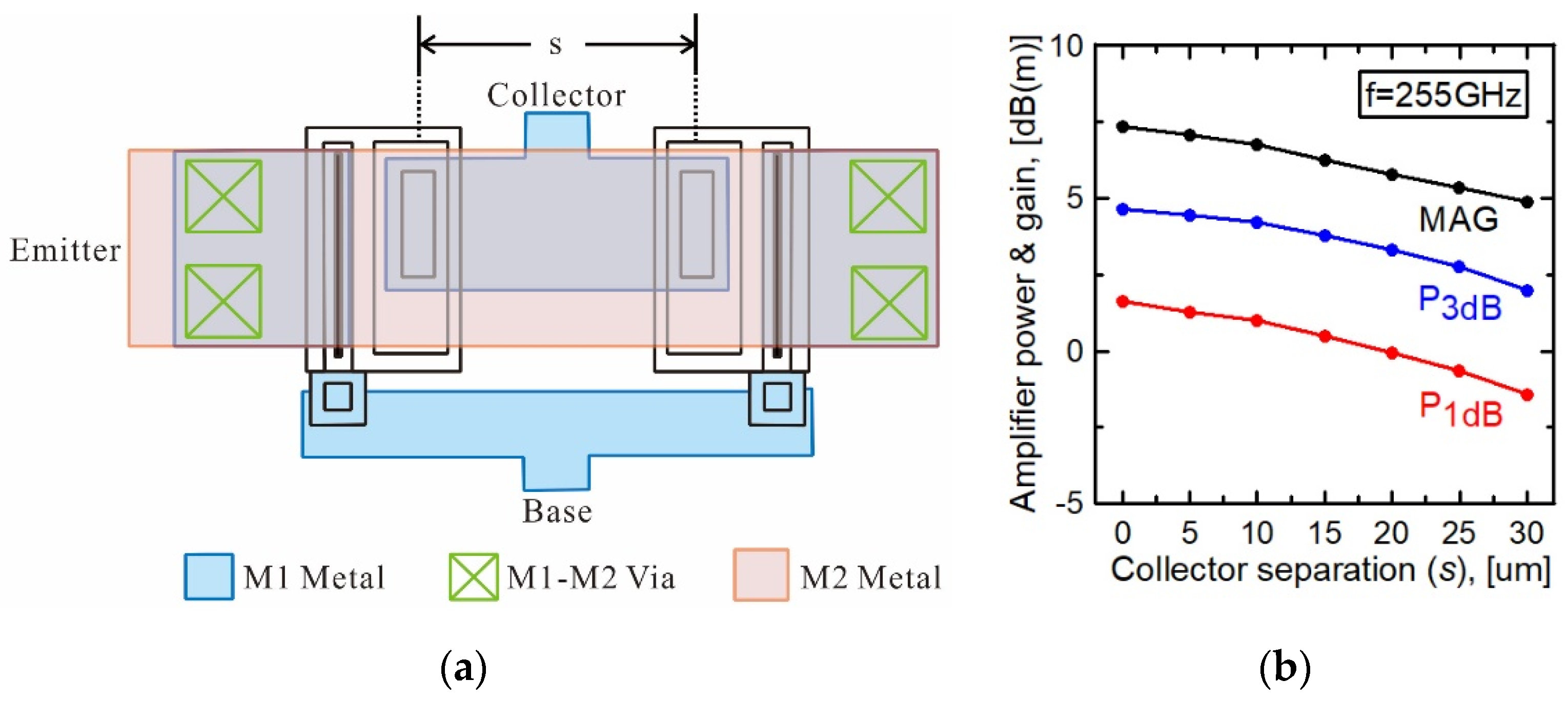
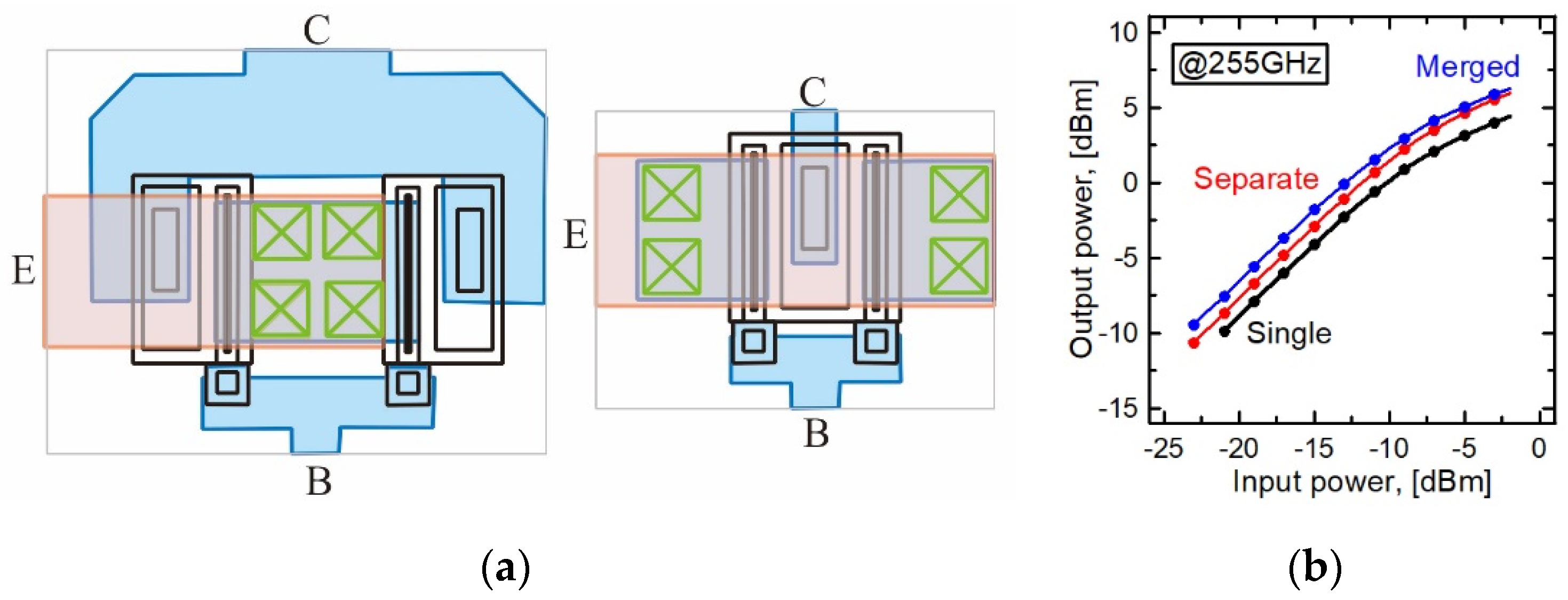
2. Dual-Finger HBT Analysis
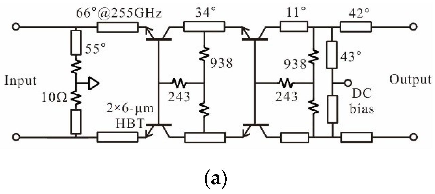
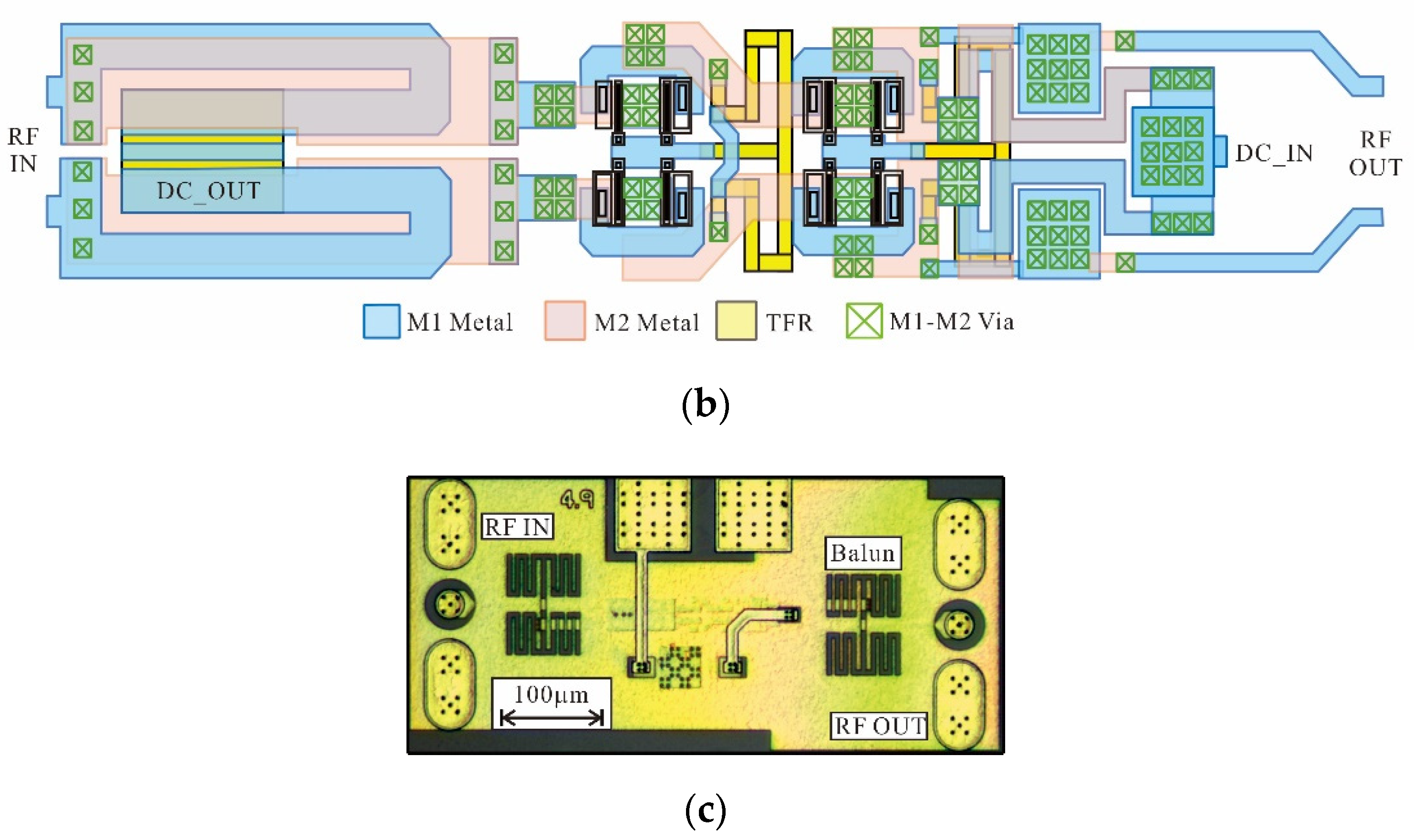
We begin the geometry analysis for the dual-finger devices with a total device width of 12 µm using the layout shown in Figure 1a. Since standard single-finger devices are recommended for guaranteed performances, modifications applied to the two-finger device layout are kept to a minimum. The layout consists of two separate 6 µm single-finger InP HBTs each with a device isolation area of 4.6 × 7.3 µm2. The analysis is carried out by using the nonlinear device model provided by Teledyne Scientific Company for the device fingers and the S-parameter data obtained from ADS Momentum simulations for the interconnected metal structures. The series parasitic inductor and resistor with a pH of 1.3 and 5.3 Ω are also added to the base of the device model. Three simulated performance parameters, the maximum available gain (MAG) and 1 and 3 dB gain-compressed output powers (P1 dB and P3 dB) for varying collector-to-collector distance (s) are plotted in Figure 1b. The results obtained under the optimum gain and power impedance matching conditions indicate that the performance worsens as the device separation is increased as the phase offset introduced by the interconnecting wiring becomes substantial. Because the adjacent isolation areas should have a minimum spacing of 2 µm, the distance between the two collector posts (s) should be at least 5 µm. In order to further decrease the separation distance to zero, we created a new geometry where two isolation areas are merged into one with a size of 6.6 × 7.3 µm2 such that the two collector posts overlap with each other. Compared to the separate-isolation device with 5-µm distance, the merged-isolation device should provide a higher MAG and a larger amount of output power even though the improvement seems marginal. However, the performance differences between the separate-isolation and merged-isolation devices should become greater as the number of fingers increases for the HBT devices.

3. Amplifier Design

Two amplifiers, each with different types of dual-finger HBT devices, are fabricated with identical matching networks. The layouts in Figure 2a show the 12 µm devices with separate and merged isolation areas. The separate-isolation device is formed by connecting two standard 6 µm single-finger HBTs, with each device flipped horizontally from the layout used in the analysis in Figure 1a. The separate-isolation device has an equivalent collector-to-collector distance (s) of 8.4 µm and has a total size of 19 × 16 µm2 including the structures in the interconnecting metal layers. The merged device, on the other hand, maintains the same layout used in the analysis in Figure 1a with a collector separation distance of zero. It is formed by sharing the collector metals of two single-finger HBTs implementing a new custom two-finger device that has zero collector-to-collector distance (s) with a total size of only 15 × 12 μm2. The performances of two types of 12 µm dual finger devices are estimated once again under ideal impedance matching conditions for the input and the output. The separate-isolation device is expected to possess an MAG at 255 GHz of 7.2 dB and the maximum frequency of oscillation (fmax) of 596 GHz, slightly worse than the values expected from a single-finger standard device. However, the 3 dB gain-compressed output power (P3 dB) of 4.3 dBm is better than that from a single-finger device by roughly 2 dB. The merged-isolation device shows similar performance with the single-finger device with an MAG and fmax of 7.4 dB and 608 GHz. The output powers are improved to a P3 dB of 4.7 dBm, resulting in an enhancement of 0.3 dB over those of the separate-isolation device.
The circuit schematic for the two-stage four-finger differential amplifier chain with a 24 μm output device periphery used in the initial stage of the design is shown in Figure 3a. The final circuit layout shown in Figure 3b contains separate-isolation devices that are to be replaced with merged devices for the second amplifier design. Both designs adopt the common-base configuration where the base terminals are self-biased from a single DC bias applied through the collector terminals using collector-base resistances of 2848 Ω per 6 μm finger. While portions of the self-bias resistors shown as 243 Ω and placed on the virtual ground have no impact on the RF performance, the 948 Ω resistors across the differential output ports lower the amplifier gain but improve the stability. Additional 10 Ω resistors are added to the emitter of the first-stage devices to further stabilize the design. A pair of defective-ground two-way baluns are added to both ends of the differential amplifier chain for connection to single-end RF probe pads. The whole differential amplifier chain is only 30 µm wide, meaning that it can be used as a building block to form a linear array in future power-combining circuit designs. Figure 3c is the photograph of the fabricated circuit showing a physical chip size of 600 × 270 µm2.

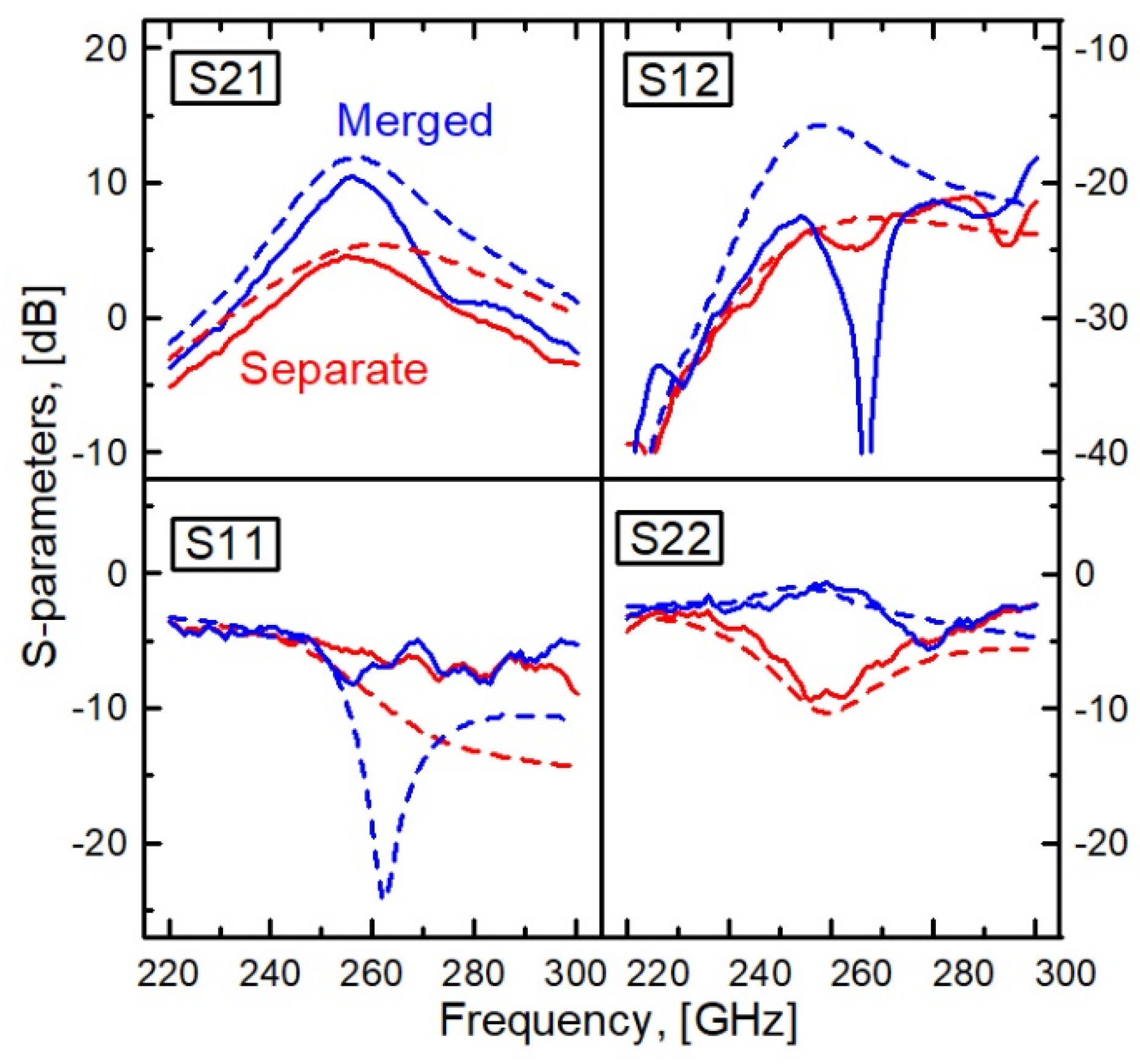
4. Measurement Results

The measured small-signal s-parameters for the two amplifiers are plotted in Figure 4 for the total bias voltage of 4 V and the total bias current of 40 mA. This bias condition translates to an adequate DC-bias for each HBT finger with a VCE of 1.76 V and IC of 10 mA. The measured data show reasonable agreements to the simulated data with no indication of oscillations in either amplifier. The separate-isolation amplifier shows a peak gain of 4.6 dB while the merged amplifier shows a peak gain of 10.5 dB at 255 GHz. While both dual-finger devices are expected to possess similar characteristics, the amplifier gains are substantially different with a difference of close to 6 dB. We suspect that the output instability for the common-base configuration [10] causes a large gain change even when the devices are connected to an identical matching network.
The power measurement is also carried out at 255 GHz where the two amplifiers possess the largest gain by using a pair of Cascade WR-3.4 RF probes, each with roughly 3 dB of insertion loss. The measured gain from the power test setup gives similar results to the small-signal gain using a network analyser as shown in Figure 5a validating the power calibration process. The output powers for separate and merged device amplifiers are plotted in Figure 5b. Because of the low small-signal gain of only 4.6 dB, the power saturation is barely noticeable for the separate-device amplifier. However, the measured 1 dB gain-compressed output power is significantly larger at −1.9 dBm for the merged amplifier compared to −8.3 dBm for the separate amplifier. The maximum output powers under the full saturation condition are 4.4 and 5.2 dBm for separate and merged amplifiers, respectively, confirming that the merged devices indeed produce a better power performance, as indicated in our analysis.

5. Conclusions

Table 1 shows a list of 250 nm InP HBT amplifiers operating above 200 GHz that have been reported in the past decade. Although SiGe amplifier developments are also beginning to make some progress in terms of frequency [11] and output power [12], InP devices are still the dominant technology in most terahertz integrated circuit research. The output power of an amplifier is proportional to the total periphery of the output devices, and it is imperative to increase the size of the output device. Thus, we have investigated a custom two-finger device by modifying standard single-finger HBTs by merging two device isolation areas. The amplifier tested at 255 GHz confirms that the device with the merged isolation area offers better power performances compared to the bulkier separate-isolation device amplifier. Although amplifiers using four-finger devices were introduced earlier, as listed in Table 1, our device maintains three transistor terminals, allowing the formation of a differential configuration. Currently, our amplifiers possess a total output periphery of only 24 μm, with a smaller power density per device length due to the use of the stabilization resistors. A new amplifier design using a four-finger device with an improved stability is currently being investigated.

Author Contributions

Investigation, formal analysis, data curation, and original draft preparation, Y.K.K.; investigation and data curation, Y.W.K.; supervision, project administration, and funding acquisition, M.K. All authors have read and agreed to the published version of the manuscript.

Funding

This research was supported by the National Research Foundation of Korea (NRF) grant funded by the Korea government (MSIT) (No. 2021R1A2C2009528).

Acknowledgments

The chip fabrication was supported by the IC Design Education Center (IDEC), Korea.

Conflicts of Interest

The authors declare no conflict of interest.

References

  1. Rodwell, M.; Le, M.; Brar, B. InP bipolar ICs: Scaling roadmaps, frequency limits, manufacturable technologies. Proc. IEEE 2008, 96, 271–286. [Google Scholar] [CrossRef]
  2. Urteaga, M.; Griffith, Z.; Seo, M.; Hacker, J.; Rodwell, M.J.W. InP HBT technologies for THz integrated circuits. Proc. IEEE 2017, 105, 1051–1067. [Google Scholar] [CrossRef]
  3. Yu, H.J.; Choi, S.H.; Jeon, S.; Kim, M. 300 GHz InP HBT amplifier with 10 mW output power. Electron. Lett. 2014, 50, 377–379. [Google Scholar] [CrossRef]
  4. Kim, M. Broadband coupled-line balun on a defected ground structure. Microw. Opt. Technol. Lett. 2012, 54, 2575–2577. [Google Scholar] [CrossRef]
  5. Kim, J.; Jeon, S.; Kim, M.; Urteaga, M.; Jeong, J. H-band power amplifier integrated circuits using 250-nm InP HBT technology. IEEE Trans. Terahertz Sci. Technol. 2015, 5, 215–222. [Google Scholar] [CrossRef]
  6. Li, L.; Ke, W. Integrated planar spatial power combiner. IEEE Trans. Microw. Theory Tech. 2006, 54, 1470–1476. [Google Scholar]
  7. Griffith, Z.; Urteaga, M.; Rowell, P.; Pierson, R.; Field, M. Multi-finger 250-nm InP HBTs for 220-GHz mm-wave power. In Proceedings of the 2012 International Conference on Indium Phosphide and Related Materials, Santa Barbara, CA, USA, 27–30 August 2012; pp. 204–207. [Google Scholar]
  8. Griffith, Z.; Urteaga, M.; Rowell, P. 180–265 GHz, 17–24 dBm output power broadband, high-gain power amplifiers in InP HBT. In Proceedings of the 2017 IEEE MTT-S International Microwave Symposium (IMS), Honololu, HI, USA, 4–9 June 2017; pp. 973–976. [Google Scholar]
  9. Ahmed, A.S.; Soylu, U.; Seo, M.; Urteaga, M.; Rodwell, M. A compact H-band Power Amplifier with High Output Power. In Proceedings of the 2021 IEEE Radio Frequency Integrated Circuits Symposium (RFIC), Atlanta, GA, USA, 7–9 June 2021; pp. 123–126. [Google Scholar]
  10. Green, J.E.; Tozer, R.; David, J.P.R. Stability in small signal common base amplifiers. IEEE Trans. Circuits Syst. I Regul. Pap. 2012, 60, 846–855. [Google Scholar] [CrossRef]
  11. Yoon, D.; Seo, M.; Song, G.; Kaynak, M. 260-GHz differential amplifier in SiGe heterojunction bipolar transistor technology. Electron. Lett. 2017, 53, 194–196. [Google Scholar] [CrossRef]
  12. Sarmah, N.; Aufinger, K.; Lachner, R.; Pfeifer, U.R. A 200–225 GHz SiGe power amplifier with peak P sat of 9.6 dBm using wideband power combination. In Proceedings of the ESSCIRC Conference 2016: 42nd European Solid-State Circuits Conference, Lausanne, Switzerland, 12–15 September 2016. [Google Scholar]
Figure 1. (a) Dual-finger device geometry used in the performance analysis, and (b) estimated devices performances vs. separation distance between two collector posts (s).
Electronics 11 02614 g001
Figure 2. (a) Layouts for fabricated dual-finger HBTs with separate and merged device isolation areas, and (b) their simulated optimum power performances.
Electronics 11 02614 g002
Figure 3. Differential amplifier chain design showing (a) initial circuit schematic, (b) final layout, and (c) photograph of the fabricated full amplifier circuit.
Electronics 11 02614 g003aElectronics 11 02614 g003b
Figure 4. S-parameters for amplifiers using merged-isolation devices (blue) and separate-isolation devices (red) showing measured (solid) and simulated (dashed) results.
Electronics 11 02614 g004
Figure 5. (a) Measured power gain using −15 dBm of input power (solid) plotted together with small-signal data (dashed), and (b) measured output power vs. input power.
Electronics 11 02614 g005
Table 1. List of amplifiers operating above 200 GHz using 250 nm InP HBT technology.
RefYearFreq. [GHz]Psat
[dBm]
Circuit
Size
[μm²]
Finger
Size [μm]
No. FingersNo. Dev.Output
Perphery [μm]
Power/μm
[μW]
[3]20143009.80.59 × 0.5251840239
[5]201530113.50.67 × 0.68611696233
[8]2017200242.14 × 1.586416384650
[9]202127016.80.89 × 0.5464496498
This work,
separate
20222554.40.59 × 0.2762224115
This work,
merged
20222555.20.59 × 0.2762224138
Publisher’s Note: MDPI stays neutral with regard to jurisdictional claims in published maps and institutional affiliations.

