Article

Fundamental Investigation of Wave Propagation inside IC-Striplines upon Excitation with Hertzian Dipole Moments

by
Dominik Kreindl
1,2,*,
Thomas Bauernfeind
2,
Bernhard Weiss
1,
Christian Stockreiter
1,
Suresh Kumar Yenumula
1,
Bhuvnesh Narayanan
1 and
Manfred Kaltenbacher
2
1
ams OSRAM Group, 8141 Premstaetten, Austria
2
Institute of Fundamentals and Theory in Electrical Engineering, Graz University of Technology, 8010 Graz, Austria
*
Author to whom correspondence should be addressed.
Electronics 2022, 11(16), 2488; https://doi.org/10.3390/electronics11162488
Submission received: 21 June 2022 / Revised: 5 August 2022 / Accepted: 7 August 2022 / Published: 10 August 2022
(This article belongs to the Special Issue Electromagnetic Interference, Compatibility and Applications)

Abstract

:
To characterize the electromagnetic compatibility (EMC) of integrated circuits (ICs), especially the radiated emissions in the near field, transversal electromagnetic cell (TEM cell) or IC-stripline measurements (IEC 61967) are utilized. Due to the ongoing miniaturization and the increasing operating frequencies, accurate EMC characterization of ICs is becoming more important to achieve first-time-right designs. In order to avoid expensive redesigns, the prediction of these measurements in terms of a simulation workflow would be of high interest. Because of the high computational burden needed to conduct 3D full-wave finite element (FEM) simulations of both the device under test (DUT) and the measurement system, an equivalent representation of the DUT by means of analytical incident fields, such as Hertzian dipole moments, can be considered. In order to develop an order-reduced model of this kind, it is essential to have a solid understanding of the coupling and wave propagation effects inside the measurement systems. In the present paper, a fundamental investigation of the coupling paths between an IC-stripline and electric or magnetic dipole moments is presented and the results are compared to the existing analytical models. The results show that these analytical models, originally developed for TEM cells, are only partially valid for IC-striplines. It has also been shown that even for simple test structures, such as loop and monopole antennas, the representation in terms of one single dipole moment is insufficient.

1. Introduction

In the past few years, the demand for integrating high-power laser modules into mobile or wearable electronic devices has increased strongly. Many integrated optical sensor modules of such devices use vertical cavity surface-emitting lasers (VCSELs). VCSELs are widely used as an infrared (IR) light source for applications such as time of flight (TOF) cameras or structured light systems, e.g., face recognition, automotive in-carbine sensing or light detection and ranging (LIDAR) [1,2,3,4]. Nevertheless, the operation of VCSELs demands fast pulsed currents of high amperage and fast rise times. Therefore, the integration of this technology into densely packed electronic systems bears the risk of electromagnetic interference (EMI) between the VCSEL driver circuit and other integrated systems. Possible victims of the interference are 5G antennas, wireless communication or sensor systems. Due to the high integration density and the increased operating frequencies, the EMC characterization in terms of measurement is becoming nearly impossible, especially when resolving different coupling paths. For this reason, an attempt is made to develop numerical field simulation methodologies to describe the electromagnetic behavior of ICs and packages before fabrication.
For the measurement of IC radiated emission (RE), transversal electromagnetic waveguides, such as TEM cells (IEC 61967-2) and IC-striplines (IEC 61967-8), are utilized [5,6]. In order to avoid redesigns, a simulation workflow for the prediction of the outcome of these measurements would be of high interest. However, a 3D full-wave FEM simulation of both the described measurement system and the DUT is very resource-consuming in terms of computational power. For this reason, an equivalent analytical representation of the DUT can be considered. The high currents of the above described VCSEL driver circuits are conducted to the diode via bond wires. These wires can be considered as a half-current loop over a ground plane and by thinking of the image theory [7], we can obtain a full current loop. Assuming that these current loops are the main RE sources, a reduced model, consisting of an array of electric and magnetic dipoles to represent a VCSEL system, is considered. A summarized literature study on these dipole moment methods can be found in [8]. An accurate order reduced model of this kind would decrease the computational burden and simulation time to predict the described measurements significantly. The usage of purely analytical formulas for the output voltages of the measurement systems would even decrease it by magnitudes.
It turns out that analytic descriptions of this kind have already been developed for TEM cell measurements. There, the purpose was to find an equivalent representation of the DUT to enable far-field (FF) open area test site (OATS) simulations of the DUT. Measurement methodologies to extract an array of equivalent dipole moments have been developed for two-port TEM cells by Sreenivasiah et al. [9,10,11] and Koepke et al. [12] and also for GTEM cells by Wilson [13]. All these models have in common that they are based on the field theory of guided waves [14,15], which will be described in more detail in Section 2. For instance, it is well known from the theories that for rectangular waveguides, the orientation and position of the moments strongly influence the voltage generation on the output of the test system. For example, horizontal current loops inside an IC cannot be characterized correctly by those measurement methods if the IC is mounted onto an EMC test PCB. This has been previously identified as a weakness [16].
These formulas are valid as long as the dipole sources are placed in the center of the upper or lower chamber of the TEM cell and only the dominant TEM mode exists. In this paper, an evaluation of this analytic model and the influence of the positioning of current sources inside IC-striplines are conducted by the means of full-wave FEM simulations and measurements.
The rest of this paper is organized as follows: Section 2 introduces the analytic dipole theory, the IC-stripline method, and the used test PCBs. Section 3 shows the measurement and simulation results and finally, in Section 4, the conclusion of this work is presented.

2. Measurement Methods, Theory and Test Structures

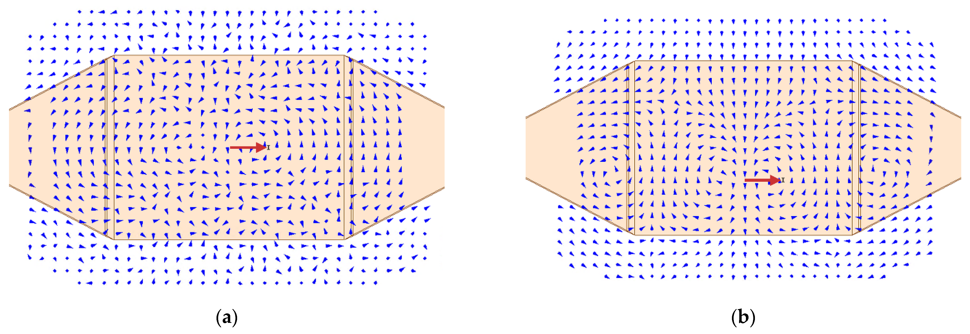
2.1. IC-Stripline Method

For EMC characterization of electronic equipment, TEM cells have been commonly used for quite a while [17]. To be able to not only characterize system level equipment, such as a notebook, but also just a single IC, smaller TEM cells with a cutout for standardized EMC test PCBs are utilized both for immunity and emission tests (IEC 61967 and IEC 62132). Since the immunity test with this kind of cells requires expensive amplifiers to generate the required electric field strength (E-field) inside the cell, the IC-stripline method was introduced [18], which is now also used for emission tests [6]. Figure 1 shows the cross-sections of both measurement systems. The physical background of both systems is similar. The DUT, connected to the EMC test board, generates an electromagnetic field, which propagates along the septum in form of a TEM wave towards the coax connectors on both sides. At the junction, the mode converts into a coaxial mode and travels further towards the 50 Ω termination resistance of either a termination resistor or a measurement device, such as a vector network analyzer (VNA) or an EMI receiver.

2.2. Hertzian Dipole Theory
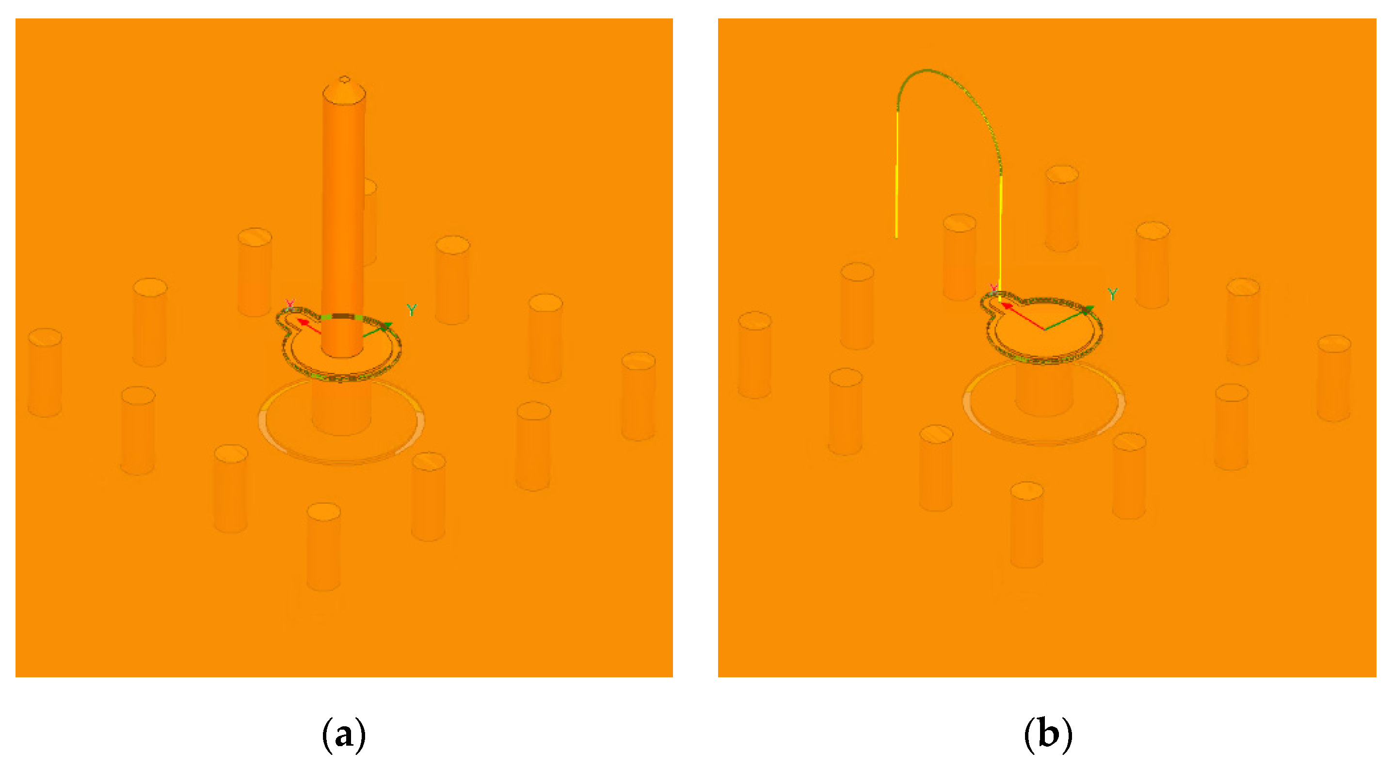
A Hertzian electric dipole can be thought of as an infinitesimal small straight wire antenna, with l << λ, ∀ λ, where l is the length of the dipole and λ is the wavelength. Additionally, the diameter of this wire is considered infinitesimal small as well (a << λ, ∀ λ). The antenna is excited with a uniform current distribution of constant current amplitude I 0 along the length of the antenna. This gives an electric dipole moment I 0 l of the dimension Am along the wire length.
For a magnetic Hertzian dipole on the other hand, a straight wire is not considered, but a closed circular wire loop with constant current amplitude I 0 . In this case, a magnetic dipole moment,
I m l = j S ω μ 0 I 0 ,
of the dimension Vm is evoked perpendicular to the loop area [19]. In this expression, j is the imaginary unit, S is the loop area, ω is the angular frequency and μ 0 is the vacuum permeability.
The emitted spherical field components of these radiators in free space, when positioned in the coordinate center aligned with the z-axis, can be found via the magnetic vector potential A and the electric vector potential F (see [19] as an example).
An electric dipole can be demonstrated by the following equations:
E ϕ = H r = H θ = 0 E r = Z 0 I 0 l c o s θ 2 π r 2 ( 1 + 1 j k r ) e j k r E θ = j Z 0 k I 0 l s i n θ 4 π r ( 1 + 1 j k r 1 k 2 r 2 ) e j k r H ϕ =   j k I 0 l s i n θ 4 π r ( 1 + 1 j k r ) e j k r
A magnetic dipole can be demonstrated by the following equations:
E r = E θ = H ϕ = 0 E ϕ = j k I m l s i n θ 4 π r ( 1 + 1 j k r ) e j k r H r = I m l c o s θ 2 π Z 0 r 2 ( 1 + 1 j k r ) e j k r H θ =   j k I m l s i n θ 4 π Z 0 r ( 1 + 1 j k r 1 k 2 r 2 ) e j k r
In these expressions, Z 0 is the characteristic impedance of free space, r is the distance of the investigated sphere from the source and k is the phase constant.
It can be observed from (1) that the strength of the magnetic dipole moment is frequency dependent when excited with constant wire current amplitude I 0 , while the electric dipole moment is not. This has great influence on the behavior of infinitesimal dipole moments inside a TEM cell. The analytical description of these behaviors is as follows [9,10,11].
By considering a rectangular waveguide with perfect electric side walls with the 0th order TEM mode propagating inside in positive and negative axial direction (x-direction), the field components are given by
E ( ± ) = ( a b ) E 0 ( ± ) H ( ± ) = ( a b ) H 0 ( ± ) .
In (4), a and b are the amplitudes of the propagating mode in positive and negative x-direction and E 0 and H 0 are the field components of this mode, described by
E 0 ( ± ) = ( z e 0 z + y e 0 y ) e j k 0 x H 0 ( ± ) = ± ( z h 0 z + y h 0 y ) e j k 0 x .
In (5), z and y are unity vectors, e 0 z ,   e 0 y , h 0 z , h 0 y are the transverse field components given for a certain geometry of a wave guide when excited with 1 W and k 0 is the phase constant of the TEM mode. To describe the relation between the amplitudes of the propagating mode and an exciting current source inside the wave guide, Lorentz reciprocity theorem can be used [14,15], shown by the following equation:
( a b ) = 1 2 Ω ( J · E 0 ( ) ) d Ω .
By thinking of an infinitesimal short current source, (6) can be rewritten as
( a b ) = 1 2 m e · E 0 ( )
and m e = J Ω represents an electric dipole moment. By considering an infinitesimal thin filament current, the strength of the dipole moment can be rewritten as I 0 l from (2).
If the current source, however, forms a closed loop and if one replaces J with I 0 , (6) can be written as
( a b ) = 1 2 I 0 S E 0 ( ) · d l = 1 2 I 0 S c u r l E 0 ( ) · n d S = 1 2 ( j ω μ 0 ) H 0 ( ) · m m
using Stoke’s theorem, Faraday’s law of induction and by introducing the magnetic dipole moment m m = I 0 S n . This also gives the relation to I m l in (1) and (3), which is as follows: I m l ω μ = | m m | = I 0 S . By expressing the magnetic field via
H 0 ( ± ) = ± x × E 0 ( ± ) Z 0
and using superposition of an electric and magnetic dipole source by deploying (5) to (7) and (8), one can obtain the following equation:
( a b ) = 1 2 ( m e · e 0 ± j k 0 m m · ( x × e 0 ) )
with
e 0 = ( z e 0 z + y e 0 y ) .
This implies that, when positioned in the center of the waveguide y-wise ( y = 0 e 0 y = 0 ), only the z-component of an electric dipole and the y-component of a magnetic dipole will contribute to the amplitudes of a and b. When it is not centered y-wise, e 0 y is not zero; therefore, the y-component of an electric dipole and the z-component of a magnetic dipole will also contribute to the amplitudes. However, dipole components aligned with the propagation direction (x-direction) will never have any influence on a and b according to this analytic model. The presented model is restricted by the assumption that only the zeroth order mode is able to propagate inside the waveguide, and therefore is not valid for higher frequencies that allow higher order modes. Typically, the frequency range for which TEM cells and IC-striplines are suited, according to the manufacturer, comply with this limit. The frequency range for the IC-stripline used in this work is 150 kHz to 3 GHz.
Due to the similar underlying operating principle of TEM cells and IC-striplines, the use of this model could be interesting for IC-striplines as well. Nevertheless, because of the non-rectangular cross section and the smaller dimensions of IC-striplines, this analytic model cannot be used without further investigation. Therefore, the behavior of dipoles for IC-striplines shall be investigated in terms of numerical simulations and measurements.

2.3. Test PCBs

To evaluate the analytical behavior of the dipole moments by measurement, an approach was made to build electrically small geometries onto two-layer test PCBs that behave as similar as possible to the theoretical moments, according to [20]. The PCB blanks can be observed in Figure 2. They feature just one central signal via with a signal pad on the top and bottom layer, respectively. The rest of the PCB top and bottom area consists of a ground plane, largely protected by solder resist, which is not taken into consideration for this investigation. On the top layer, a SMA connector is soldered to the signal pad and ground accordingly. The small test geometries are placed on the bottom layer. To represent an electric dipole, a small piece of wire is soldered onto the bottom layer signal pad vertically. To represent a magnetic dipole and also the bond wires of VCSEL drivers as described in Section 1, a bond wire is bonded in a loop from the bottom layer signal pad to the bottom layer ground plane, as shown in Figure 3. In both cases it is assumed that through the effects of the image theory due to the large ground area, the behavior of the small geometries will represent the dipoles accordingly. The PCBs are further referred to as E-PCB for the electric dipole and H-PCB for the magnetic dipole.
To confirm the dipole-like behavior of the test PCBs, a H-field scan of both PCBs was carried out and compared to the analytically calculated values using (2) and (3). The x- and y-component of the field were measured individually with the aid of a near field probe. The schematic test setup can be observed in Figure 4 and the results can be observed in Figure 5, Figure 6, Figure 7 and Figure 8. The intention of this experiment was to prove the dipole-like field distribution of the test PCBs. Therefore, the comparison between measurement and analytical solution is only performed qualitatively and provided without a magnitude scale. The used frequency for this experiment was 1 GHz. The measured area was bounded by the innermost row via stitching of the PCB, as can be observed from Figure 3a. The field distribution that was measured and analytically computed shows good qualitative agreement, and therefore confirms the usability of the test PCBs for these investigations. Nevertheless, there are noticeable deviations between the plots, which may be explained as follows:
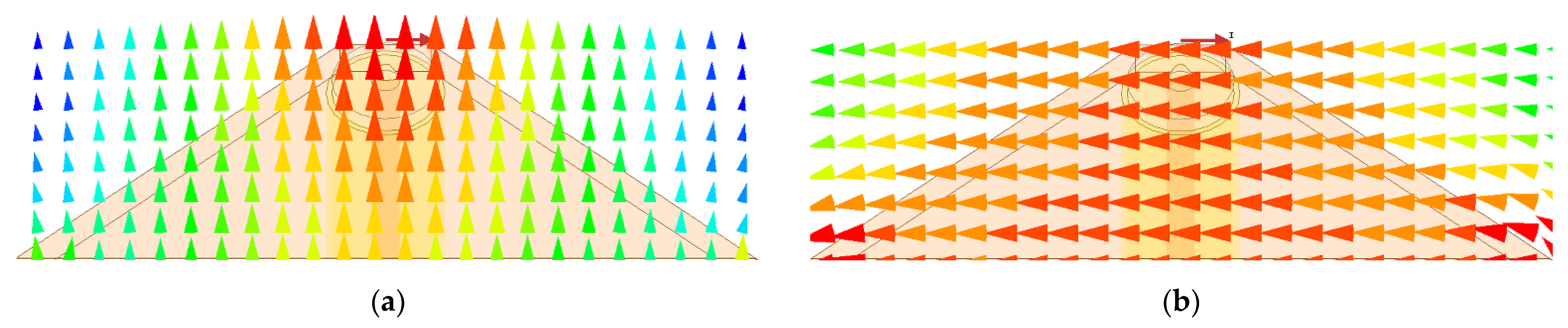
  • Offset of the minimum field strength from the center in Figure 6.
    The field distribution in Figure 5 assumes a perfectly positioned dipole (centered in x- and y-direction and aligned with the z-axis). The soldered-on wire piece of the E-PCB is not orientated perfectly perpendicular to the x-y-plane, and therefore produces a field distribution of similar shape as an electric dipole but shifted in the x and y direction.
  • Non-touching low-magnitude arcs in Figure 8a.
    In contrast to Figure 7a, the areas of low magnitude are not touching at y = 0 but form two non-touching arcs in Figure 8a. This can be explained by the bond wire not being perfectly aligned to the edges of the PCB, while the probe tip was aligned with the PCB during the measurement. Because of this rotation angle between the wire and the measurement coil, the minimum of the measured field is not located directly above the wire.
  • Differences in general between Figure 5 and Figure 6 or Figure 7 and Figure 8, respectively.
    It should be noted that the two test PCBs do not behave in a similar way to perfect Hertzian dipole sources due to their non-infinitesimal small size. Consequently, there will be additional effects, evoked by the PCB.

2.4. Simulation Models

To conduct 3D FEM investigations on the behavior of dipole moments inside an IC-stripline, a simulation model of the investigated IC-stripline was implemented. To validate the model, simulation models of the test PCBs were also made and the conducted S-parameter simulations were compared to VNA-measurements of the setup (Figure 9, Figure 10 and Figure 11). The investigated frequency range was 150 kHz to 3 GHz, in agreement with [6].

3. Results

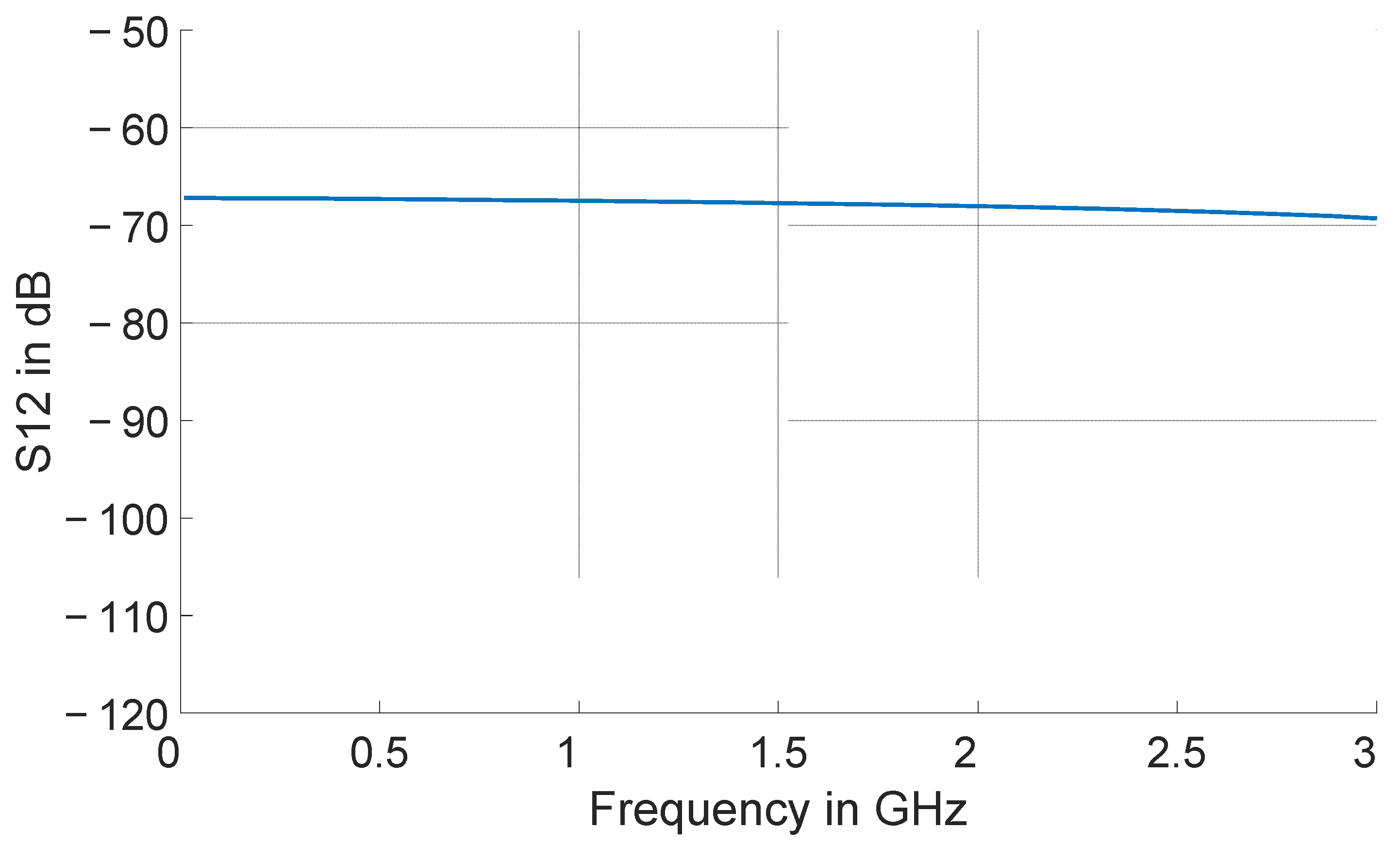
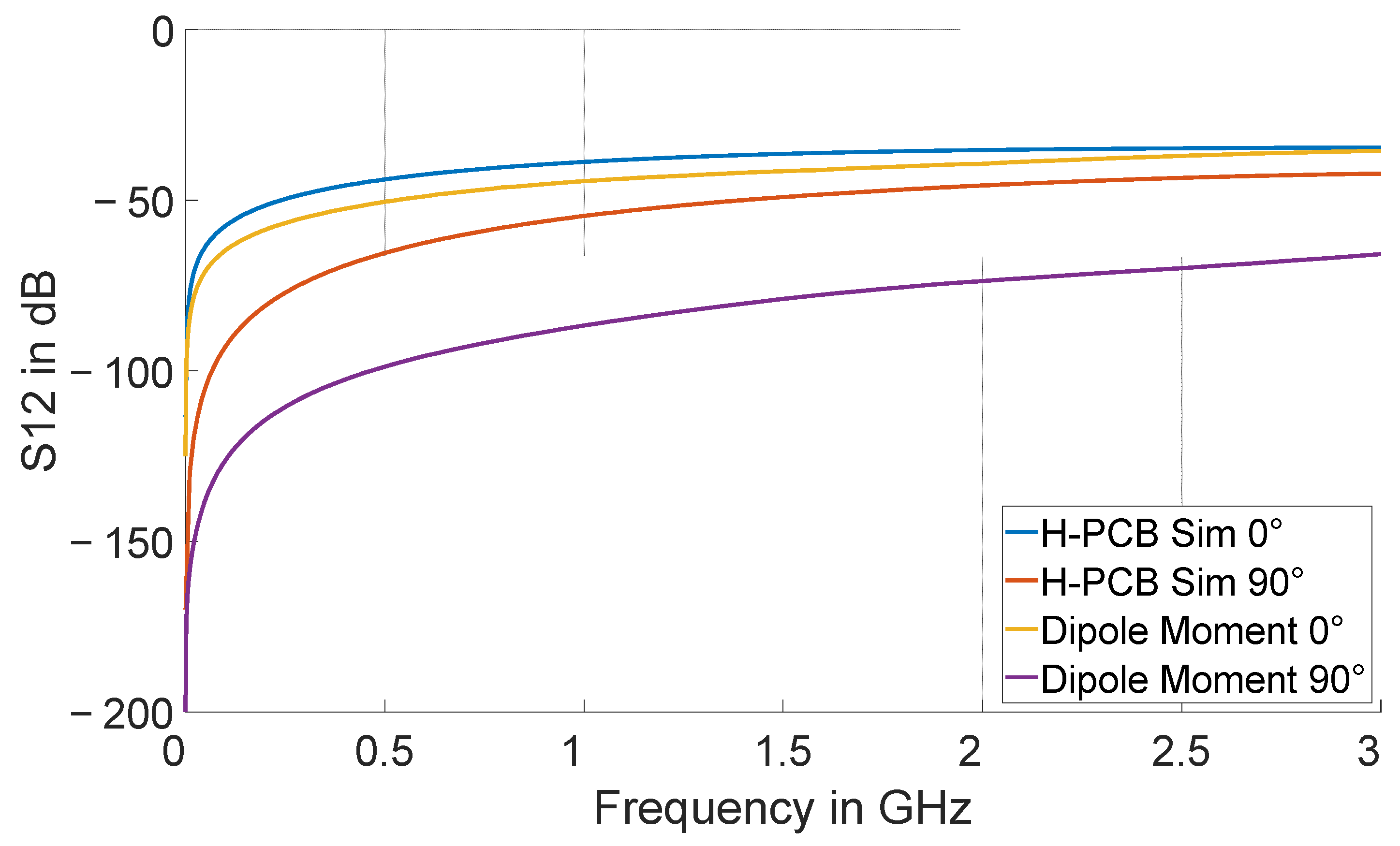
3.1. Comparison of Test PCB Measurements and Full Wave Simulation

Figure 12 and Figure 13 show the comparison of the measured coupling factor S12 (see Figure 9) with the simulated values. For the H-PCB, two measurements were carried out, one with the bond wire being parallel to the orientation of the septum and one with the bond wire being perpendicular to the septum. They are referred to as the 0° and 90° case. The simulation results were compared with the measurement results of two different IC-striplines of the same construction type to compare them with regard to manufacturing imperfections.
To match the measurement, the realistic structure of the bond wire had to be modeled in a very accurate way. The real bond wire was not aligned perfectly to the PCB edges, but rotated by 4°. This rotation angle must also be introduced in the simulation models.
The results show very good agreement, and therefore confirm the usability of the simulation models as a fundament for further investigations. The deviation between the measurements and simulation is within 3 dB, which can be considered a good result if the noticeable deviation between the two IC-striplines is taken into account.

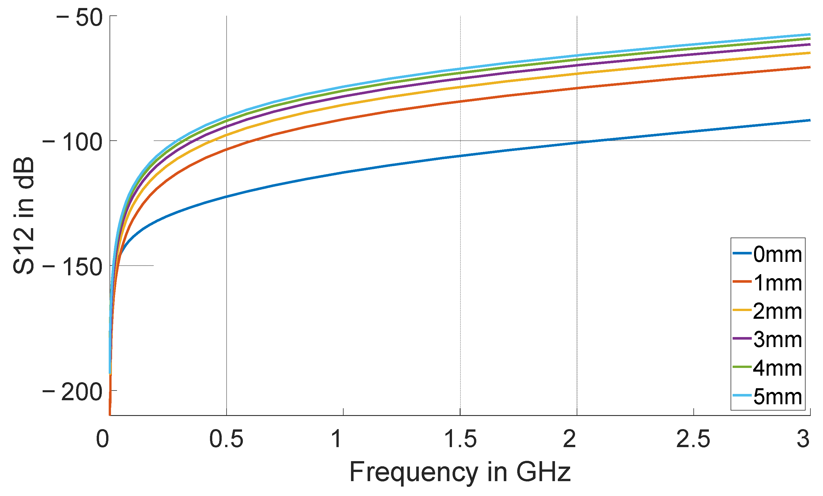
3.2. Dipole Moments inside IC-Stripline

Before the simulation can be carried out, one has to think about the magnitude of the inserted dipole waves to be able to compare the results with the test PCBs. For this purpose, a dipole extraction method as proposed in [21] could be used. For that, the VNA measurement, as shown in Figure 9, could be extended by a third port connected to the 2nd connector of the IC-stripline, instead of the 50 Ω termination resistor. In this way, the phase difference between the two measured IC-stripline port voltages is not lost; therefore, this measurement methodology can replace a hybrid junction because the measurement of both ports is synchronized [21].
In the first step, however, the test PCBs are compared to a single dipole moment. For this, the current amplitude I 0 in (2) and (3) of the dipole moments is searched for. For the E-PCB, it is difficult to find the correct equivalent dipole intensity due to the triangle shaped current distribution on the wire piece [19]. Therefore, the results of the dipole moment experiment can only be compared to the E-PCB measurement and simulation qualitatively. For the H-PCB, on the other hand, the current flow in the bond wire can be extracted through simulations, and then a moment according to (1) can be introduced.
The chosen position for the dipole moments is along the z-axis in the center of the test PCB for the electric dipole and perpendicular to the bond wire area plane in the center between the two points, where the wire is bonded to the copper for the magnetic dipole. One must note that this position is not in the center of the H-PCB, and therefore not in the center of the IC-stripline. Figure 14 shows the positions of the dipole moment on the test PCBs. Figure 15 and Figure 16 show the results of this experiment for an electric dipole moment in z direction and a magnetic one in x- and y-direction.
Because a comparison to the analytical model is aspired, the bond wire in the H-PCB simulation is now idealized and parallel to the PCB edges (not rotated by 4°). Therefore, the curve for the 90° case is different in Figure 13 and Figure 16. For the 0° case, this has no noticeable impact.
One must note that a direct S-parameter simulation cannot be conducted in this experiment, since the excitation is not carried out via a wave-port. Instead, the voltage or power at the stripline ports has to be computed in terms of a post-processing routine. The methodology to compare the S-parameter curves of the test PCBs and the measured port voltages of the dipole moment is the following:
  • Set the dipole strength according to the geometry of the test PCB and the simulated current amplitude I 0 , when exiting the port with 0 dBm;
  • Compute the root mean square value of the output port voltage and convert the result to dBV;
  • Calculate the power of the output port with
    d B m = d B V 10 l o g 10 ( 50 Ω ) + 30 .
This value can then be compared to S-parameters.
It can be observed in Figure 15 that for the electric dipole, the coupling factor is approximately constant over a wide frequency range. This matches very well with the analytical model described by (10). The curve is only provided for frequencies above 10 MHz because at lower frequencies, simulation errors occurred that could not be resolved up to now. Since the fundamental operating frequencies of VCSEL pulse currents are typically above this value, the results are considered sufficient for this work. It can be further observed that the curve shape does not match the E-PCB simulations or measurements at all when comparing Figure 12 and Figure 15. The reason for this is that with voltage excitation, as used in the measurements and the E-PCB simulations, it is not possible to provide a constant dipole current amplitude I 0 . Because this current is strongly frequency dependent, it is not possible to generate a constant electric dipole moment over the investigated frequency range with this test structure.
For the H-PCB, on the other hand, the curve shapes of the H-PCB and the dipole moment are very similar, as shown in Figure 16. This becomes even clearer when looking at on a double logarithmic scale (Figure 17). The change in steepness for the 90° case is clearly observable for both curves. While the magnitude of the curve for the magnetic dipole fits the curve for the H-PCB in the 0° case rather well with the estimated excitation intensity for I 0 , in the 90° case, the H-PCB coupling factor is significantly underestimated by the dipole moment.
Looking at (1), the analytical model predicts a coupling factor, which increases linearly with the frequency for the 0° degree case and with no coupling at all for the 90° case. The results for the 0° case fulfill the analytical prediction quite well. For the 90° case, however, contrary to the analytic model, there is a noticeable coupling factor. Although in the range of under −80 dB over the whole frequency range, at higher frequencies, the magnitude is in a range that could be measured by standard EMC laboratory equipment.
In the next step, the sensitivity of the coupling factor with regard to the position of the magnetic dipole inside the IC-stripline is investigated. When shifting the dipole moment parallel along the y-axis in the 90° case, the analytic model predicts that there should not be any influence on the coupling factor. The model predicts no coupling at all at any position along the y-axis according to (10). The FEM results for this experiment in the 90° case can be observed in Figure 18 and Figure 19.
It can be observed that only a slight shift outside the center has a large influence. The explanation for this behavior is found when looking at the field distribution inside the IC-stripline. For the 0° degree case, the propagating TEM mode can be observed in Figure 20 and the Poynting vector distribution can be observed in Figure 21. The Poynting vector distribution of the 90° case can be observed in Figure 22. It is observed that in the 0° case, the Poynting vector (and therefore the power flow) points towards the connectors, while in the 90° case, no power flow towards the connectors exists. When shifting the moment away from the center in 90° case, the curls of the Poynting vector field are also not centered; therefore, a component pointing towards the connectors exists (Figure 22b). This effect is also observable in Figure 23. In the 0° case (Figure 23a), the current density is visible on the surface of the inner conductor of the coax connector, whilst in the 90° case, it is not.
A position shift in x- and z-direction was also carried out but since the influence on the coupling factors is less significant, these cases are not further investigated.

4. Discussion and Conclusions

This paper attempts to compare the behavior of dipole moments inside IC-striplines with test geometries and analytic formulas originally developed for TEM cells. It has been shown that for an electric dipole, it is not possible to build a test structure that delivers a constant electric dipole moment over the investigated frequency range, due to the non-uniform current density. For the test structure that represents a magnetic dipole moment, it was possible to replicate the curve shapes of the test structure with just one dipole moment. It was also possible to show that the coupling factor of a single bond wire is heavily dependent on its orientation in relation to the septum, as suggested by the analytical models. However, the results further show that even for a very simplistic test structure, one single dipole moment alone is not sufficient to match the curves either qualitatively or quantitatively. Therefore, for the prediction of radiated emission measurements of bond wires that conduct high currents, more sophisticated equivalent DUT representation models have to be developed. It has been further shown that other than in the analytic model, the position of a magnetic dipole moment has strong influence on the coupling factor when placed parallel to the direction of wave propagation. This behavior is assumed to be caused by the non-rectangular cross-section of the waveguide and needs to be further investigated in future work.

Author Contributions

Methodology, D.K.; software, D.K., S.K.Y. and B.N.; investigation, D.K.; writing—original draft preparation, D.K.; writing—review & editing, T.B., B.W. and M.K.; supervision, T.B., B.W., C.S. and M.K.; funding acquisition, T.B., C.S. and M.K. All authors have read and agreed to the published version of the manuscript.

Funding

This research received no external funding.

Acknowledgments

Supported by the TU Graz Open Access Publishing Fund.

Conflicts of Interest

The authors declare no conflict of interest.

References

  1. Zhou, D.; Seurin, J.-F.; Xu, G.; Zhao, P.; Xu, B.; Chen, T.; Van Leeuwen, R.; Matheussen, J.; Wang, Q.; Ghosh, C. Progress on High-Power High-Brightness VCSELs and Applications; Lei, C., Choquette, K.D., Eds.; SPIE: San Francisco, CA, USA, 2015; p. 93810B. [Google Scholar]
  2. Seurin, J.-F.; Zhou, D.; Xu, G.; Miglo, A.; Li, D.; Chen, T.; Guo, B.; Ghosh, C. High-Efficiency VCSEL Arrays for Illumination and Sensing in Consumer Applications; Choquette, K.D., Guenter, J.K., Eds.; SPIE: San Francisco, CA, USA, 2016; p. 97660D. [Google Scholar]
  3. Warren, M.E.; Block, M.K.; Dacha, P.; Carsonn, R.F.; Podva, D.; Helms, C.J.; Maynard, J. Low-Divergence High-Power VCSEL Arrays for Lidar Application. In Vertical-Cavity Surface-Emitting Lasers XXII; Choquette, K.D., Lei, C., Eds.; SPIE: San Francisco, CA, USA, 2018; p. 14. [Google Scholar]
  4. Warren, M.E. Automotive LIDAR Technology. In Proceedings of the 2019 Symposium on VLSI Circuits, Kyoto, Japan, 9–14 June 2019; pp. C254–C255. [Google Scholar]
  5. IEC 61967-2; Integrated Circuits Measurement of Electromagnetic Emissions, 150 kHz to 1 GHz, Part 2: Measurement of Radiated Emissions-TEM Cell and Wideband TEM Cell Method. International Electrotechnical Commission: Geneva, Switzerland, 2005.
  6. IEC 61967-8; Integrated Circuits-Measurement of Electromagnetic Emissions-Part 8: Measurement of Radiated Emissions-IC Stripline Methode. International Electrotechnical Commission: Geneva, Switzerland, 2013.
  7. Balanis, C.A. Advanced Engineering Electromagnetics; WILEY Intersience: Hoboken, NJ, USA, 1989. [Google Scholar]
  8. Ramesan, R.; Madathil, D. Modeling of Radiation Source Using an Equivalent Dipole Moment Model. PIER B 2020, 89, 157–175. [Google Scholar] [CrossRef]
  9. Sreenivasiah, I.; Chang, D.C.; Ma, M.T. Characterization of Electrically Small Radiating Sources by Tests inside a Transmission Line Cell; Rep. NBS TN 1017; US Department of Commerce, National Bureau of Standards: Gaithersburg, MD, USA, 1980.
  10. Sreenivasiah, I.; Chang, D.C.; Ma, M.T. A “Method of Determining the Emission and Susceptibility Levels of Electrically Small Objects Using a TEM Cell; Rep. NBS TN 1040; US Department of Commerce, National Bureau of Standards: Gaithersburg, MD, USA, 1981.
  11. Sreenivasiah, I.; Chang, D.; Ma, M. Emission Characteristics of Electrically Small Radiating Sources from Tests Inside a TEM Cell. IEEE Trans. Electromagn. Compat. 1981, EMC-23, 113–121. [Google Scholar] [CrossRef]
  12. Koepke, G.H.; Ma, M.T. A New Method for Determining the Emission Characteristics of an Unknown Interference Source. In Proceedings of the 1982 IEEE International Symposium on Electromagnetic Compatibility, Santa Clara, CA, USA, 8–10 September 1982; pp. 1–6. [Google Scholar]
  13. Wilson, P. On correlating TEM cell and OATS emission measurements. IEEE Trans. Electromagn. Compat. 1995, 37, 1–16. [Google Scholar] [CrossRef]
  14. Collin, R.E. Field Theory of Guided Waves. In The IEEE/OUP Series on Electromagnetic Wave Theory, 2nd ed.; IEEE: Piscataway, NJ, USA, 1991; ISBN 978-0-87942-237-0. [Google Scholar]
  15. Simonyi, K. Theoretische Elektrotechnik; VEB Deutscher Verlag der Wissenschaften: Berlin, Germany, 1977. [Google Scholar]
  16. Fiori, F.; Musolino, F.; Pozzolo, V. Weakness of the TEM cell method in evaluating IC radiated emissions. In Proceedings of the 2001 IEEE EMC International Symposium. Symposium Record. International Symposium on Electromagnetic Compatibility (Cat. No.01CH37161), Montreal, QC, Canada, 13–17 August 2001; pp. 135–138. [Google Scholar]
  17. Fang, W.; Li, Z.; Chen, R.; Huang, Q.; Shao, W.; Tian, X.; Wang, L.; En, Y. Orientation Effect of the Electromagnetic Field Coupling for Device in a TEM Cell. IEEE Trans. Microw. Theory Tech. 2022, 70, 980–991. [Google Scholar] [CrossRef]
  18. Koerber, B.; Trebeck, M.; Mueller, N.; Klotz, F. IC-stripline: Anew proposal for susceptibility and emission testing of ICs. In Proceedings of the 6th International Workshop on Electromagnetic Compatibility of Integrated Circuits, Torino, Italy, 28–30 November 2007; pp. 125–129. [Google Scholar]
  19. Balanis, C.A. Antenna Theory, Analysis and Design; WILEY Intersience: Hoboken, NJ, USA, 2003. [Google Scholar]
  20. IEC 61967-8; Integrated Circuits–Measurement of Electromagnetic Immunity–Part 1: General Conditions and Definitions. International Electrotechnical Commission: Geneva, Switzerland, 2015.
  21. Pan, S.; Kim, J.; Kim, S.; Park, J.; Oh, H.; Fan, J. An equivalent three-dipole model for IC radiated emissions based on TEM cell measurements. In Proceedings of the 2010 IEEE International Symposium on Electromagnetic Compatibility, Fort Lauderdale, FL, USA, 25–30 July 2010; pp. 652–656. [Google Scholar]
Figure 1. Cross-sections: (a) TEM cell; (b) IC-stripline.
Electronics 11 02488 g001
Figure 2. Test PCB blank: (a) top view (b) bottom view.
Electronics 11 02488 g002
Figure 3. Test PCBs: (a) E-PCB with an electrically short (<3.75 GHz) monopole of length l = 4 mm; (b) H-PCB with an electrically short (<2.2 GHz) bond-wire of length l 1 ≈ 6.7 mm.
Electronics 11 02488 g003
Figure 4. Schematic sketch of the test setup for the near field scan experiment.
Electronics 11 02488 g004
Figure 5. Analytic solution for the H-field of an electric Hertzian dipole in the measurement plane in dB-scale: (a) x-component of the H-field; (b) y-component of the H-field.
Electronics 11 02488 g005
Figure 6. Measured H-field of the E-PCB in dB-scale: (a) x-component of the H-field; (b) y-component of the H-field.
Electronics 11 02488 g006
Figure 7. Analytic solution for the H-field of a magnetic Hertzian dipole in the measurement plane in dB-scale: (a) x-component of the H-field; (b) y-component of the H-field.
Electronics 11 02488 g007
Figure 8. Measured H-field of the H-PCB with dB-scale: (a) x-component of the H-field; (b) y-component of the H-field.
Electronics 11 02488 g008
Figure 9. Schematic sketch of the test setup for the test PCB VNA measurements.
Electronics 11 02488 g009
Figure 10. Simulation model of the used IC-stripline: (a) 3D section view of the model; (b) 3D view of the septum group with two cutting planes.
Electronics 11 02488 g010
Figure 11. Simulation models of the test PCBs: (a) E-PCB; (b) H-PCB.
Electronics 11 02488 g011
Figure 12. Measurement results of the VNA measurements of the E-PCB mounted in the IC-stripline for two different IC-striplines of the same type compared to the simulation results of the E-PCB.
Electronics 11 02488 g012
Figure 13. Measurement results of the VNA measurements of the H-PCB mounted in the IC-stripline for two different IC-striplines of the same type compared to the simulation results of the H-PCB in 0° and 90° rotation case.
Electronics 11 02488 g013
Figure 14. Simulation model of the test geometries on the test PCBs with the presumed dipole moment position and direction represented by the black vectors: (a) E-PCB and the electric dipole moment; (b) H-PCB and magnetic dipole moment.
Electronics 11 02488 g014
Figure 15. Behavior of an electric dipole moment when positioned inside an IC-stripline perpendicular to the stripline lid and the septum plane.
Electronics 11 02488 g015
Figure 16. Behavior of a magnetic dipole moment with presumed constant amplitude I 0 inside an IC-stripline compared to the H-PCB simulations.
Electronics 11 02488 g016
Figure 17. Behavior of a magnetic dipole moment inside an IC-stripline compared to the H-PCB with a double logarithmic scale.
Electronics 11 02488 g017
Figure 18. Influence of a position shift of the magnetic dipole away from the center in y-direction inside an IC-stripline for the 90° case.
Electronics 11 02488 g018
Figure 19. Influence of a position shift of the magnetic dipole away from the center in y-direction inside an IC-stripline different frequencies in the 90° case.
Electronics 11 02488 g019
Figure 20. Field distribution on the vertical sectional plane in Figure 10b when excited with a magnetic dipole moment according to the 0° case: (a) E-field distribution; (b) H-field distribution.
Electronics 11 02488 g020
Figure 21. Poynting vector distribution on the horizontal sectional plane in Figure 10b when excited with a magnetic dipole moment according to the 0° case; red: magnetic dipole moment; blue: Poynting vector.
Electronics 11 02488 g021
Figure 22. Poynting vector distribution on the horizontal sectional plane in Figure 10b when excited with a magnetic dipole moment according to the 90° case; red: magnetic dipole moment; blue: Poynting vector: (a) no offset of the moment with respect to the strip line center; (b) 5 mm offset of the moment with respect to the strip line center.
Electronics 11 02488 g022
Figure 23. Surface current density on the septum and the inner coaxial cable conductors of an IC-stripline when excited with a magnetic dipole moment: (a) in the 0° case; (b) in the 90° case.
Electronics 11 02488 g023
Publisher’s Note: MDPI stays neutral with regard to jurisdictional claims in published maps and institutional affiliations.

