Article

A Fully Polarity-Aware Double-Node-Upset-Resilient Latch Design

1
Department of Electrical and Computer Engineering, University of Washington, Seattle, WA 98195, USA
2
Department of Electronic Engineering, Kyung Hee University, Yongin 17104, Korea
*
Author to whom correspondence should be addressed.
Electronics 2022, 11(15), 2465; https://doi.org/10.3390/electronics11152465
Submission received: 27 June 2022 / Revised: 18 July 2022 / Accepted: 2 August 2022 / Published: 8 August 2022
(This article belongs to the Special Issue Radiation Tolerant Electronics, Volume II)

Abstract

:
Due to aggressive scaling down, multiple-node-upset hardened design has become a major concern regarding radiation hardening. The proposed latch overcomes the architecture and performance limitations of state-of-the-art double-node-upset (DNU)-resilient latches. A novel stacked latch element is developed with multiple thresholds, regular architecture, increased number of single-event upset (SEU)-insensitive nodes, low power dissipation, and high robustness. The radiation-aware layout considering layout-level issues is also proposed. Compared with state-of-the-art DNU-resilient latches, simulation results show that the proposed latch exhibits up to 92% delay and 80% power reduction in data activity ratio (DAR) of 100%. The radiation simulation using the dual-double exponential current source model shows that the proposed latch has the strongest radiation-hardening capability among the other DNU-resilient latches.

1. Introduction

Recent advances in scaling down technology have led to a substantial decrease in supply voltage and node capacitance, resulting in a smaller amount of critical charge, the minimum charge necessary to maintain a logic state. This implies that a soft error caused by single-event upset (SEU) may occur not only in harsh radiation environments at high altitudes but also at the terrestrial level [1]. Considering the decreasing feature size in the current nanometer technology, multiple-node-upset (MNU) is more likely to occur because of charge sharing among nodes [2]. An empirical study reported that 40-nm flip-flops implemented using single-node upset (SNU)-hardened dual-interlocked memory cell (DICE) [3] do not entirely prevent the soft error and exhibit only approximately 30% better cross sections compared with non-radiation hardened flip-flops [4]. Thus, recent research on radiation hardening by design (RHBD) has focused on the double-node-upset (DNU)-hardened designs, extending the SNU-hardened latches as primitive circuit elements.
The DNU-hardened latch designs can be classified into three circuit elements: the Muller C-element (MCE) [5,6], DICE [7,8], and Schmitt-trigger (ST) cell [9]. The MCE-based DNU latches [5,6] are capable of blocking SEU propagation to adjacent nodes by changing the high-impedance state of the MCE outputs when the input nodes suffer from SEU. The output’s floating state may cause state flipping at system level when the system accesses them. Because of charge sharing between the access node and the floating output node, the dynamic voltage ripple can flip the state of the floating node. The DICE-based DNU latches extend the DICE to a delta-like [7] or a donut-like [8] architecture. When new input data are written, they consume more power and require longer write time because all the internal feedback loops should be activated and flipped. Additionally, when an upset occurs, the upset node may cause an adjacent node to transit and be suffered from the short path. The ST-based DNU latch [9] is based on the ST inverters. Therefore, it features a high noise margin, low complexity, and low power dissipation. However, its radiation hardening capability is no longer maintained when there is a ratio issue between two feedback inverters.
Recently, an approach [10] to reduce the number of SEU-sensitive nodes in DNU-hardened latches was proposed. The concept was derived from the upset polarity [11] of a CMOS logic inverter. When an energetic particle hits an off-pMOSFET, only 0-to-1 positive upset occurs at the drain node because the pMOSFET only collects positive charges. In contrast, when an energetic particle hits an off-nMOSFET, only 1-to-0 negative upset occurs at the drain node because the nMOSFET only collects negative charges. Based on this principle, a node avoids a negative upset if pMOSFETs are stacked at the node and avoids a positive upset if nMOSFETs are stacked. However, the polarity-aware latch inevitably suffers from V t h drop because the latch should stack the same type of MOSFETs. This V t h drop causes high power consumption during the state-holding phase.
This paper proposes a fully polarity-aware DNU-resilient latch (FPADRL) featuring up to a reduction of 92% delay and 80% power in data activity ratio (DAR) of 100% over existing DNU-resilient latches. Furthermore, the proposed FPADRL overcomes the limitations in the previous research works: (1) resilience to SEU without the charge sharing issue at the system level; (2) fully polarity-aware latch elements, resulting in the maximum possible number of SEU-insensitive internal nodes; (3) fewer short path cases during the SEU with lower power dissipation; (4) much robust radiation-hardening capability; (5) radiation-aware layout.
The rest of this paper is organized as follows. The proposed DNU-resilient latch is described in Section 2. Next, the simulation and evaluation results are presented in Section 3. Finally, Section 4 concludes this paper.

2. Proposed DNU-Hardened Latch Design

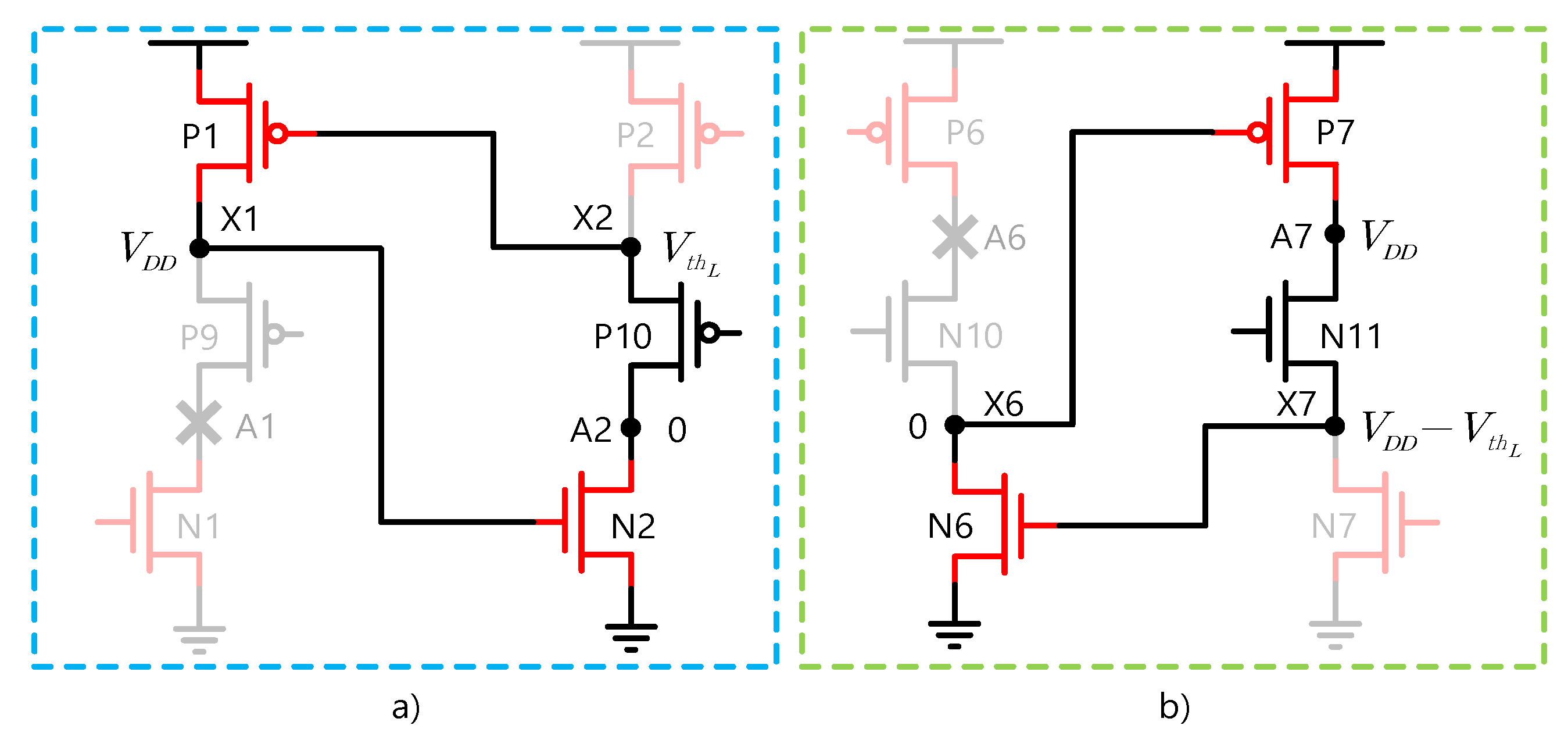
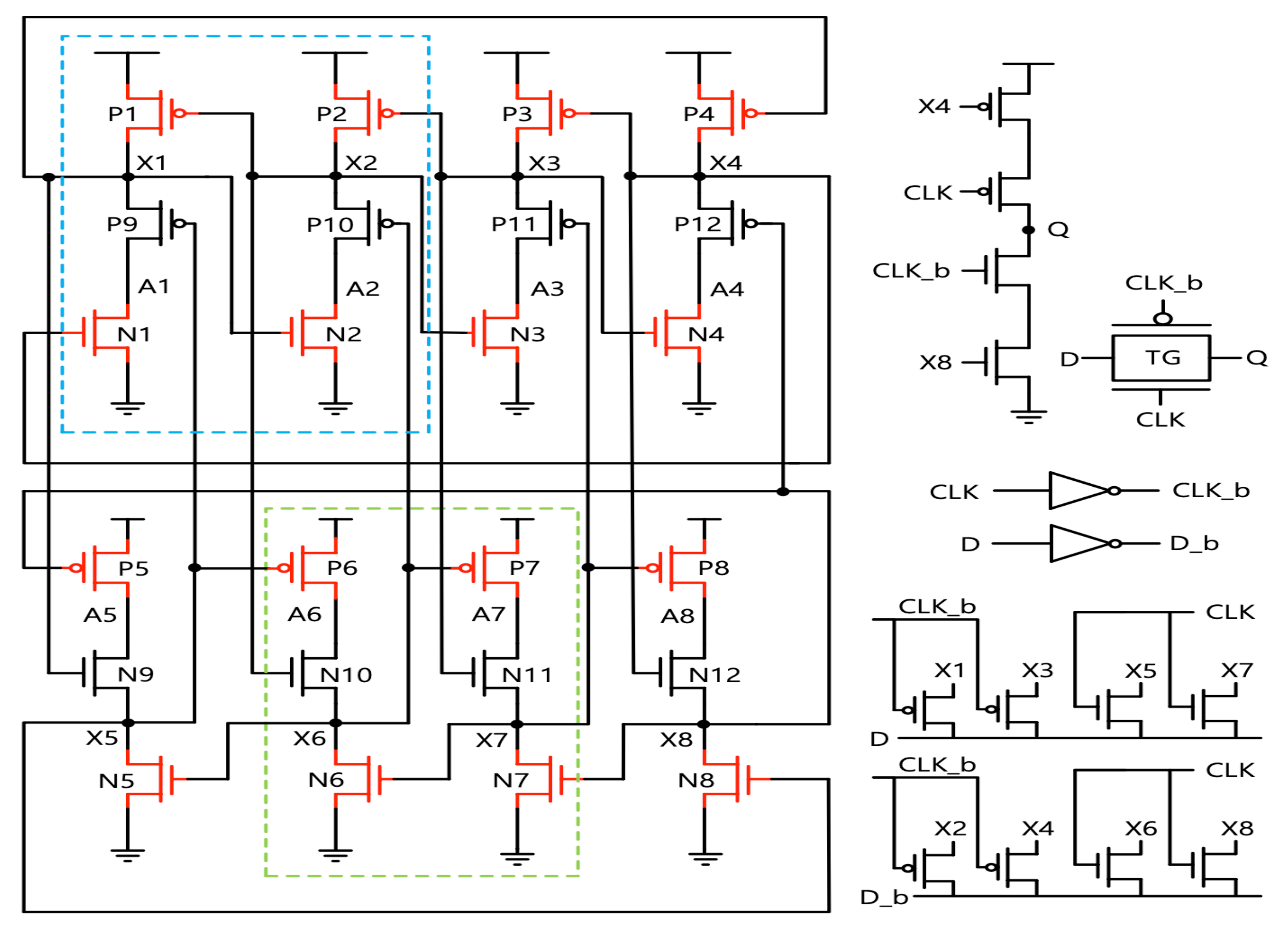
2.1. Overall Structure and Design Idea

Figure 1 shows the structure of the two latch elements in the proposed DNU-resilient latch. As shown in Figure 1a, the pMOSFET-stacked latch with the cross-coupled inverter structure has additional stacked pMOSFETs, whose operations are controlled by other latch nodes. When node X1 stores logic “1”, this node is insensitive to SEU due to the error polarity principle [11]. Node X2 is only sensitive to the 0-to-1 transition. Similarly, as shown in Figure 1b, when node X6 initially stores logic “0”, this node is insensitive to SEU, and node X7 is only sensitive to the 1-to-0 transition. When a radiation particle strikes the floating nodes A1 or A6, the initial value of these nodes may change. However, the floating nodes are not connected to any inputs; thereby, their upsets do not affect any data nodes Xn (n = 1, …, 8). The nodes between the on-transistors, such as A2 and A7, are also insensitive to SEU. Therefore, the proposed four-node latch element has only one single polarity SEU sensitive node, one floating node, and two SEU-insensitive nodes.
Simultaneously, the stacked MOSFETs play an essential role in blocking the SEU error propagation. Unlike the DICE-based latch structures, the proposed latch does not propagate the error in all SNU cases and some DNU cases due to the off-stacked transistors. Moreover, the off-stacked transistors generally block the propagation of the upset on the floating node to the data nodes. The detailed mechanism will be explained in Section 2.3.
Figure 2 shows the schematic of the proposed FPADRL. The FPADRL consists of the stacked latches shown in Figure 1, the access transistor module, and the clocked output. The upper P-stacked and lower N-stacked latch parts (PSLP and NSLP) consists of the stacked pMOSFET latches and the stacked nMOSFET latches, respectively. Thus, only positive upset occurs in the PSLP, and only negative upset occurs in the NSLP. The operations of the stacked MOSFETs are controlled by the internal nodes of the opposite latch part. Given that the two latch parts store the same data in order (i.e., X1 = X5, X2 = X6, X3 = X7, and X4 = X8), the respective node values are fed into the gate inputs of the correspondent stacked transistors to form the DICE-like dual-interlocked loops. Compared with recent research works [5,6,10], the proposed FPADRL has regular latch element architecture, and the number of sensitive nodes is maximally reduced from sixteen to eight.
Because of the stacked MOSFETs in the pull-down (up) paths, all the data nodes have the body effect, i.e., V t h drop. To reduce the leakage power by decreasing the overdrive voltage, the proposed latch uses multiple V t h transistors. The transistors shown in red in Figure 2 use high V t h , and others use low V t h . Additionally, the leakage power can be minimized by connecting one strong signal node to the off-transistor and one weak state node to the on-transistor of the output inverter. The high V t h transistors shrink the activated feedback loop time, resulting in a shorter write time compared to the DICE-based DNU latches.

2.2. Circuit Operation

The operation of the proposed latch is outlined when the input D is logic “1” (i.e., X1 = X3 = X5 = X7 = 1 and X2 = X4 = X6 = X8 = 0). Considering the error polarity, the access transistors of the PSLP are pMOSFETs, and the access transistors of the NSLP are nMOSFETs. When CLK = 1, the latch is in the transparent mode, and these access transistors drive the internal nodes. During this mode, the output Q is only driven by D through the transmission gate. The driven nodes turn on the nMOSFETs (N2, N4, N6, N8, N9, and N11) and the pMOSFETs (P1, P3, P5, P7, P10, and P12) simultaneously. As a result, nodes X1 and X3 are strong “1” state, and the nodes X2 and X4 are weak “0.” In contrast, nodes X5 and X7 are weak “1” state, and nodes X6 and X8 are strong “0.” In the CLK = 0 phase, the latch is in the hold mode, the access transistors and the transmission gate are opened, and the clock-gated inverter drives the output Q using the logic values of the internal nodes. When D = 1, the data nodes X2, X4, X5, and X7 and the floating nodes A1, A3, A6, and A8 are SEU-sensitive. Likewise, when D = 0, the latch operates complementary.

2.3. SEU-Resilience Analysis

As explained in Section 2.1, the proposed latch reduces the SEU-sensitive internal nodes as fully as possible, from sixteen to eight. Moreover, the sensitive nodes have not both-way transitions but one-way error polarity with 0-to-1 or 1-to-0 transitions. Therefore, the proposed latch has 8 SNU nodes and 28 DNU node pairs. As shown in Table 1, the proposed latch has ten different upset cases. Each case includes example node(s), SEU polarity and recovery mechanism; “↑” (“↓”) denotes 0 (1)-to-1 (0) SEU transition, “←” and “→” denote that SEU propagates to that node, “↚” and “↛” denote that SEU does not propagate to that node. Table 1 shows only the cases when D = 1. The SEU recovery of the complementary input, D = 0, has the same recovery mechanism since the circuit topology is symmetric.
When an ionizing particle strikes at the floating node, like Case 2 in Table 1, the upset does not affect data nodes since the floating node is not connected to any inputs. Considering Case 2 mechanism, Case 4 and Case 5, DNU between data node and adjacent (a) or remote (r) floating node, can be simplified to Case 1. In Case 6 and Case 7, the upset occurs on the node that controls the off-stacked transistors, so the error propagates to the adjacent data node and temporarily creates the short (s) path. However, the proposed latch can recover in these cases. For example, in Case 7, the error-propagated node X3’s voltage does not turn off N11, even though node X3 is short. Therefore, only the recover-charging current through P7 and N11 flows to node X7, causing node X3’s race to nullify by turning off P11 gradually. The recovery of node X3 results in the recovery of node X2. Like Case 8, deposited charge on a floating node A6 can be shared with a data node X6 by turning on N10. In this case, the node X5 voltage can turn on P6 and P9. However, since those weak inversion transistor currents are smaller than the strong driven currents from the neighboring transistors, the logic value of node X1 does not change, and node X6 can be recovered. The proposed latch can also recover cases when the SNU or DNU occurs at the output node Q since the proposed latch guarantees the SNU resiliency of all internal nodes. Consequently, the proposed latch is resilient to all SNU and DNU cases. The detailed transistor sizing scheme for SEU-resilience will be explained in Section 3.1.

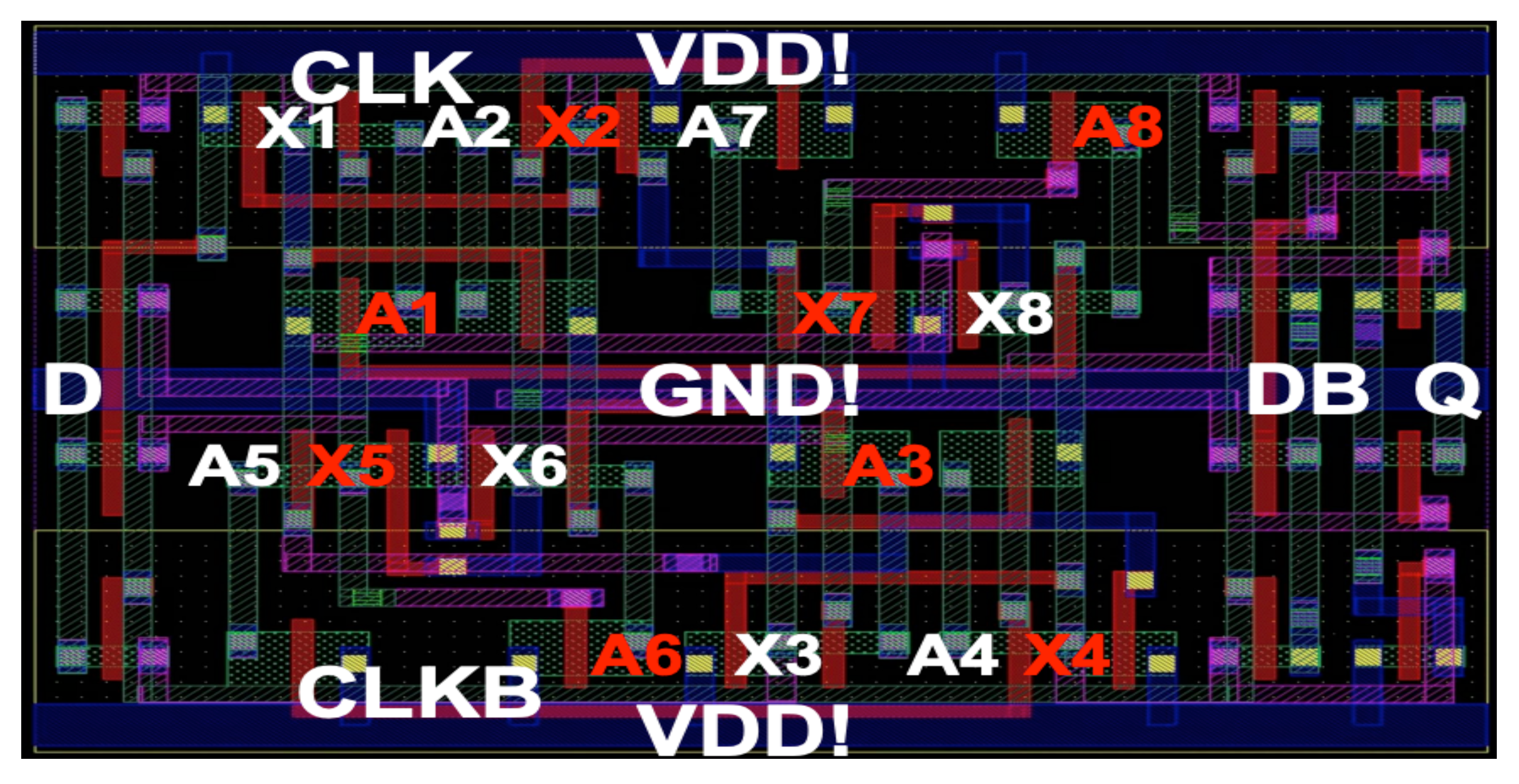
2.4. Radiation-Aware Layout

Figure 3 shows the proposed layout considering layout-level issues such as incidence angle, charge sharing (CS), and parasitic bipolar effect (PBE) [2]. Sensitive nodes are colored in orange when D = 1. The proposed layout utilizes double height cell design [12]: N-well at the top and bottom, P-well in the middle. The middle P-well acts as a canceling area between two N-wells. Based on this principle, the chance of multiple-node-upsets in different wells (severe cases such as Case 6–8) can be lowered. Moreover, our node placement can mitigate CS and PBE in sensitive data nodes. We separated NSLP’s two sensitive data nodes as far as possible in P-well. Two sensitive data nodes in PSLP are in the different N-well. To reduce the effective amount of injected charge, we placed on- and off-transistors repeatedly. Off-transistors with Ax nodes act as a strong collector, and on-transistors with Ax nodes act as a weak collector when the upset occurs on the data node. Therefore, the data node’s upset threshold increases [13]. However, we need to reconfigure the layout in more advanced technology nodes because of the polysilicon bends.

3. Evaluation Results

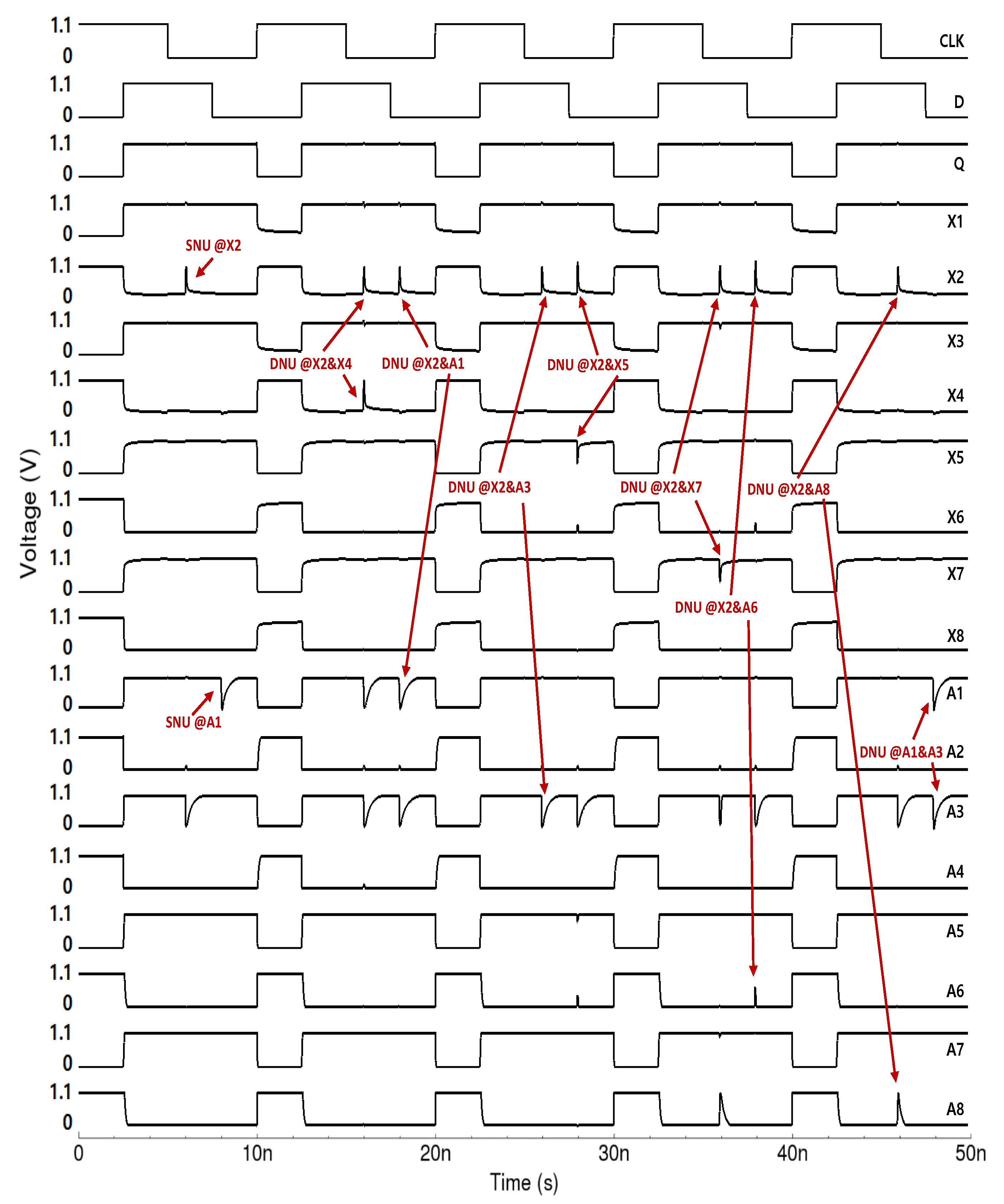
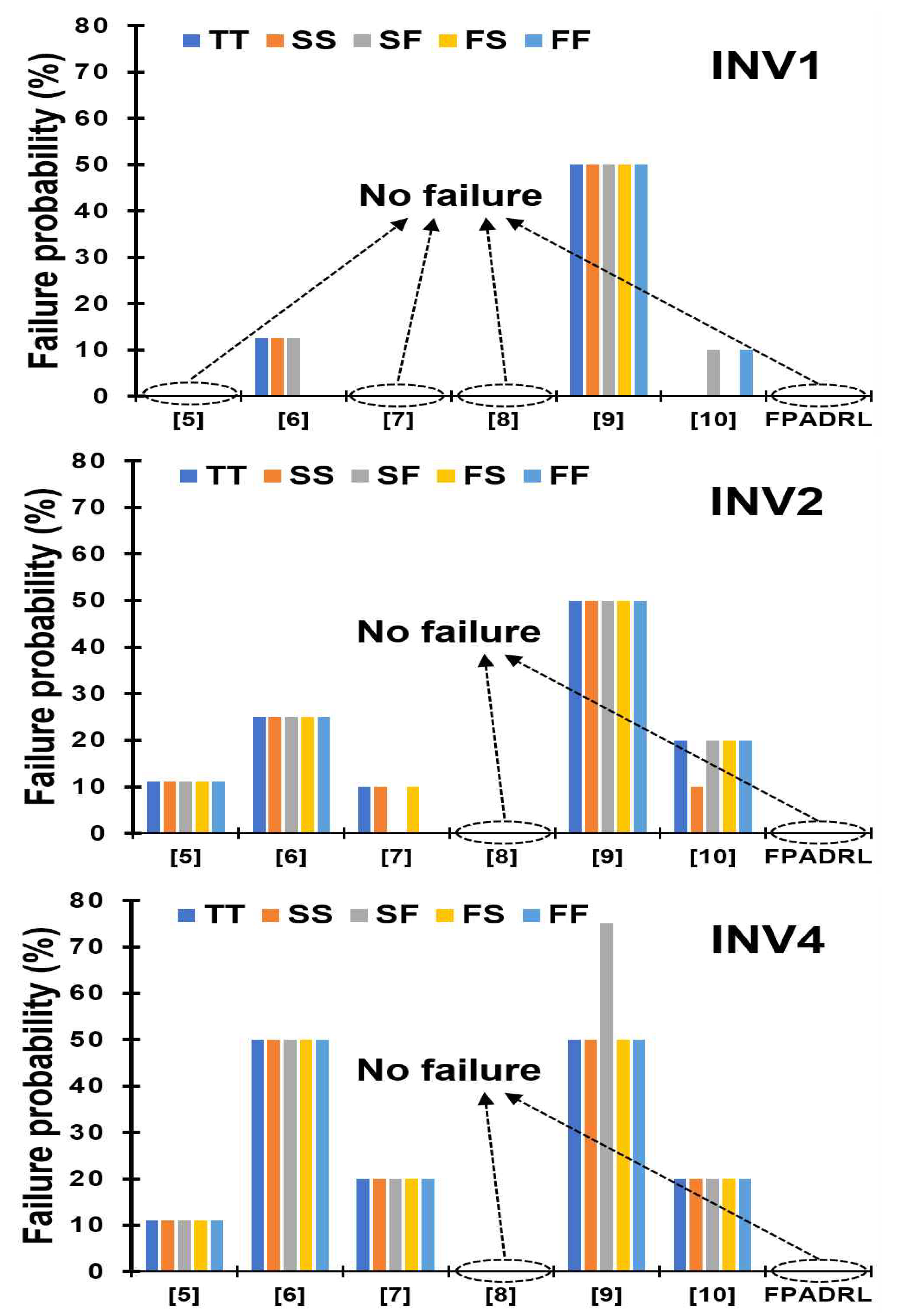
3.1. Radiation Simulation Results

The proposed latch was designed using the 45-nm NCSU CMOS technology. Due to its unique recovery process, the DICE-based latch provides a large margin of transistor sizes while keeping the SEU resilience. Therefore, we can aggressively optimize the sizes with minimum PDP. However, this approach may result in many different transistor sizes not suitable for the state-of-the-art layout. Considering both PDP and layout, we decided on smaller groups of uniform size for transistor sizes. Table 2 shows the transistor sizes, in which the aspect ratio of 1 is W/L = 90 nm/50 nm. The low (high) V t h of n(p)MOSFET are 0.322 V (−0.302 V) and 0.608 V (−0.505 V), respectively.
To validate the proposed latch’s SEU-resilience, the dual-double exponential current source [14] model was used instead of the conventional double exponential upset model because it provides a current shape similar to the actual SEU-current. The simulations were performed using Smartspice from Silvaco. Figure 4 shows the radiation simulation waveforms for all the cases in Table 1. These waveforms show that the output Q is always error-free, and all the internal nodes are recovered in all SNU and DNU cases. Therefore, it is clearly demonstrated that the proposed latch is resilient to both SNU and DNU.

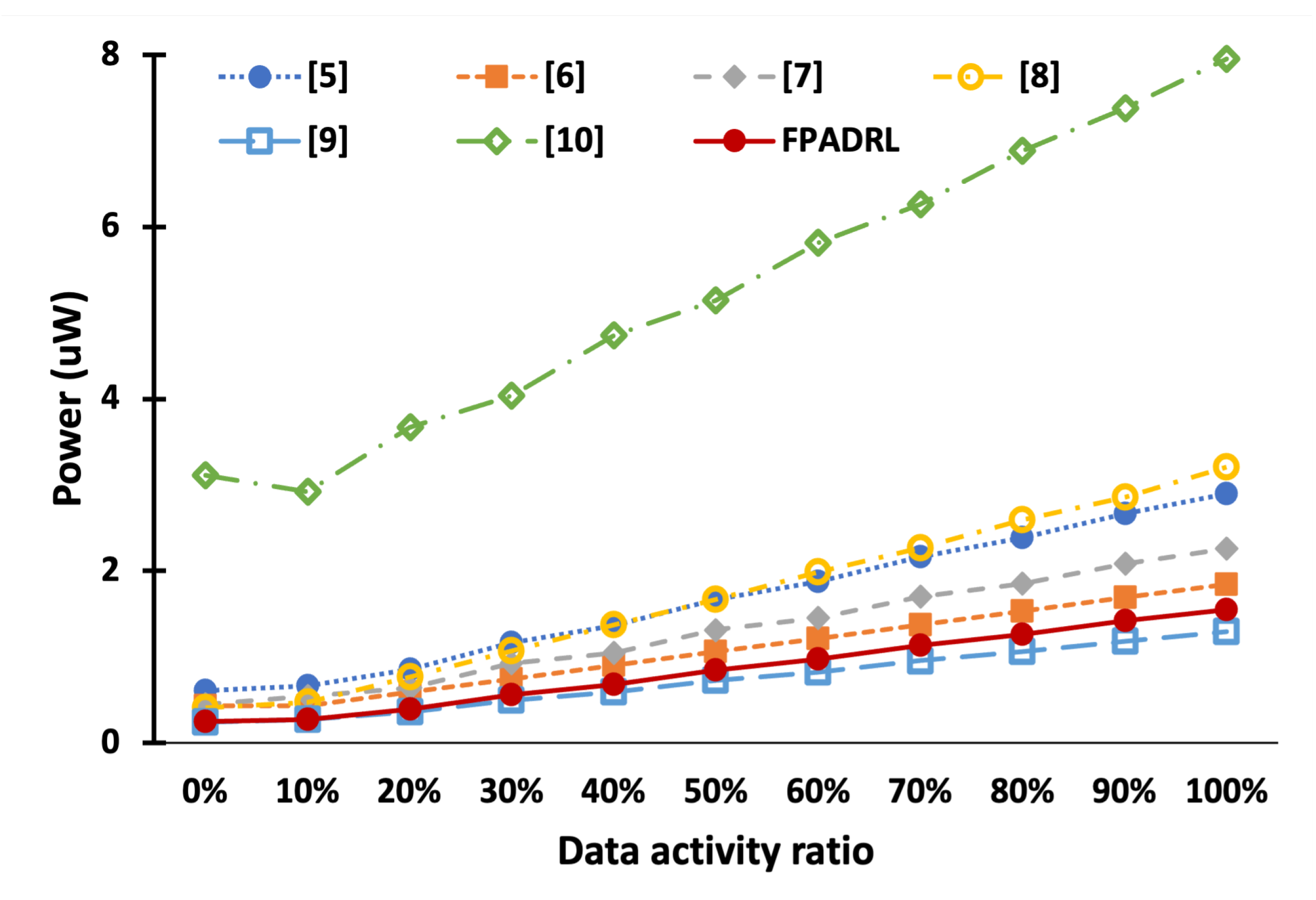
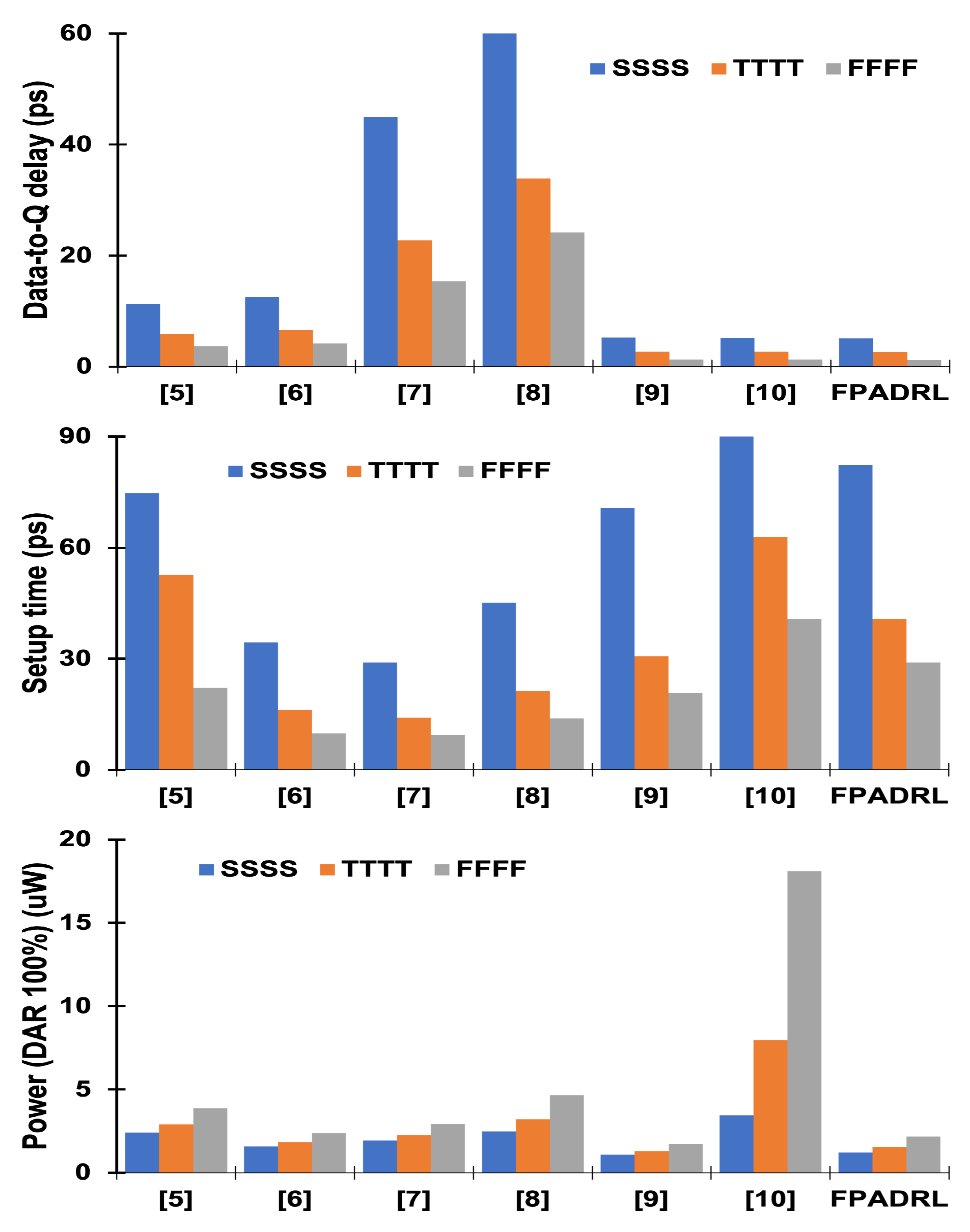
3.2. Performance Comparison and Evaluation

Table 3 shows the comparison results at the TTTT (1.1 V/25 °C/TT). Using the same technology with the proposed latch, the referred designs were re-implemented with the same size ratio the corresponding manuscripts provided. The simulation was conducted under a clock frequency of 100 MHz. The clock frequency was set enough for checking normal operation and recovery operation simultaneously.
By stacking the transistors with regular latch architecture, the proposed latch fully reduces the SEU-sensitive nodes by half from sixteen to eight. Moreover, among the eight sensitive nodes, four floating nodes are less sensitive to SEU, and the other four nodes are one-way sensitive, not both ways. The area of the proposed layout is compared based on the scaled-down results of [10]. Even though the proposed layout is radiation-aware and others are not, its regular latch architecture makes 12% less area compared with the state-of-the-art polarity-aware latch [10]. Although the number of transistors in the FPADRL is not the lowest, its layout area can be easily optimized because of its lower design complexity than regular latch architecture. In terms of delay, t d q and t s e t u p are evaluated. Power consumption profiles are divided into static power during opaque mode and dynamic power in DAR of 100%.
The MCE-based DNU latches [5,6] require extra transistors to achieve upset resilience. Fundamentally, the MCE relies on high impedance for radiation hardening. However, because of this property, the MCE-extended design usually needs a plethora of transistors for resilience. When the upset occurs, the MCE blocks not only error propagation to adjacent nodes but also the feedback path for recovery. Therefore, [5,6] consist of 66 and 48 transistors, which are the top two largest number of transistors. The more transistors used, the higher the power consumption. In terms of delay, [5,6] have a moderate speed compared to the DICE-extended design [7,8] due to directly driven output Q through the transmission gates. However, the input D should drive the nodes with large capacitance, so its delay is longer than our proposed design. As a result, [5,6] have up to 60% delay and 47% power overhead compared with the proposed FPADRL.
The DICE-extended designs [7,8] have a considerable delay and power consumption. Because they inherit DICE, the designs should activate all DICE feedback loops when the data are switching. It indicates that input D should have the large driving capability to write new data, resulting in performance penalties. Moreover, the input D does not drive the output Q directly, so the t d q delay is more considerable than other reference designs. As a result, the proposed FPADRL achieves a reduced delay and power (in DAR 100%) up to 92% and 52%, respectively, compared with [7,8].
The ST-extended design [9] has similar delay and power compared to the proposed FPADRL. The design uses the least number of transistors among the reference designs and our proposed design. However, the design is susceptible to the ratio issue. Hence, its radiation-hardening capability is weak, as presented in Section 3.3.
Lastly, the conventional polarity-aware latch [10] consumes considerable power due to its irregular cross-coupled latch structures with only single V t h transistors. By using regular latch structures and high-threshold voltage transistors to make shorter activated feedback time and to minimize the leakage power, the proposed FPADRL achieves 80% power (in DAR 100%) reduction compared with [10].
Regarding setup time, the proposed latch pales in comparison to [6,7,8,9]. Like the DICE-extended designs [7,8], FPADRL activates all feedback loops when writing new data. However, the setup performance is degraded due to the high V t h device and the stacked MOSFETs. The MCE-extended design [5] and the polarity-aware latch [10] require a longer setup time than the proposed latch because of the circuit topology for DNU-resilience and irregular latch structure.
For a more detailed evaluation of the power consumption, the comparison was made in the range of the DAR 0% to 100% at the TTTT. Figure 5 shows the proposed latch outperforms power against the MCE-based DNU latches [5,6] and the DICE-based DNU latches [7,8]. Because of the V t h drop issue, the recent polarity-aware latch [10] shows huge power consumption than all other circuits. Although the ST-based DNU latch [9] is shown to have superiority in the power over the proposed latch, the ratio issue of the ST’s recovery yields inferior radiation-hardening capability, as shown in Section 3.3.
A simulation with the process, voltage, and temperature (PVT) corner analysis was performed according to the commercial standard. The following three extreme conditions were set: (1) SSSS: 0.99 V/125 °C/SS, (2) TTTT: 1.1 V/25 °C/TT, (3) FFFF: 1.21 V/−40 °C/FF. Figure 6 shows the performance comparison with the PVT corner analysis. From the reasons described in the previous paragraph, the DICE-based DNU latches [7,8] have the most extensive t d q variation, and the MCE-based DNU latches [5,6] follow next. Although the conventional polarity-aware latch [10] has a shorter delay and smaller variation, [10] consumes more power. The ST-based latch [9] has the lowest delay and power due to its simple architecture. However, it suffers from the ratio issue for the radiation hardening. FPADRL has longer setup time in three conditions than [6,7,8,9]. Note that the setup time of the proposed latch increases significantly in the SSSS corner due to the high V t h device like [9].

3.3. Radiation-Hardening Capability Comparison

The robustness of the proposed latch against SEU was simulated and compared with those of other latches. In order to analyze the effect of robustness according to the process corner, the simulation was conducted for five corners at 1.1 V/25 °C: SS, SF, TT, FS, FF. For the comparison, different amounts of charge according to the inverter size (INVX) were injected into key node pairs of each design. Table 4 shows the peak and plateau currents of the DDECS and the total amount of charge. Given that the SEU width depends on the LET radiation [15,16], the SEU width of the INV1, INV2, and INV4 were set to be 50 ps, 100 ps, and 200 ps, respectively. The INV1’s nMOSFET size is W/L = 90 nm/50 nm and pMOSFET size is W/L = 180 nm/50 nm. The INV2 is the double size of the INV1, and the INV4 is the quadruple size of the INV1.
Using the various injection parameter settings in Table 4, the current was injected to key node pairs. The failure probability is calculated by the number of cases in which DNU are not recovered among all cases. Figure 7 shows the failure probability among the DNU-resilient latches with different corners. The ST-based [9] shows the weakest radiation-hardening capability. In contrast, the proposed FPADRL and [8] can recover every case in all corners.
Table 5 shows the recovery power at the TTTT. The recovery power is defined as the power difference between upsets and normal operation (no upsets). Although the MCE-based DNU latches [5,6] consume less recovery power than FPADRL, FPADRL overwhelms the radiation-hardening capability than [5,6] as shown in Figure 7. Unlike the DICE-based DNU latches [7,8] which are suffered from the short path when the upset occurs, the proposed latch does not create the short path in most cases due to the stacked MOSFETs. Thus, FPADRL consumes less power for recovery than [8] which has the same radiation-hardening capability.
To summarize, FPADRL is the best candidate among state-of-the-art DNU-resilient latches in a comprehensive view comparison. Although the FPADRL does not show the best performance, it has the strongest radiation-hardening capability with low recovery power.

4. Conclusions

A fully polarity-aware DNU-resilient latch with high performance and low power was proposed. The proposed latch is self-recoverable for all SNU and DNU cases. Its performance and radiation-hardening capability comparison against other latches indicate that the proposed FPADRL is performance-effective and highly robust with less overhead. Consequently, the proposed FPADRL exhibits certain advantages compared with state-of-the-art DNU-resilient latches.

Author Contributions

Conceptualization, J.-J.P., Y.-M.K. and J.K.; methodology, J.-J.P. and Y.-M.K.; software, J.-J.P. and Y.-M.K.; validation, J.-J.P., Y.-M.K. and G.-H.K.; formal analysis, J.-J.P., Y.-M.K. and J.K.; investigation, J.-J.P., Y.-M.K., G.-H.K., I.-J.C. and J.K.; resources, J.-J.P., Y.-M.K. and J.K.; data curation, J.-J.P. and J.K.; writing—original draft preparation, J.-J.P.; writing—review and editing, J.-J.P., Y.-M.K., G.-H.K., I.-J.C. and J.K.; visualization, J.-J.P., Y.-M.K. and G.-H.K.; supervision, I.-J.C. and J.K.; project administration, I.-J.C. and J.K.; funding acquisition, J.K. All authors have read and agreed to the published version of the manuscript.

Funding

This research was funded by National Research Foundation of Korea, grant number: 2019R1F1A1054130 and Institute for Information and Communications Technology Promotion, grant number: 2021001764.

Institutional Review Board Statement

Not applicable.

Informed Consent Statement

Not applicable.

Data Availability Statement

The data presented in this study are available on request from the corresponding author. The data are not publicly available due to licensing agreements.

Conflicts of Interest

The authors declare no conflict of interest.

References

  1. Pudi N S, A.K.; Baghini, M.S. Robust Soft Error Tolerant CMOS Latch Configurations. IEEE Trans. Comput. 2016, 65, 2820–2834. [Google Scholar] [CrossRef]
  2. Black, J.D.; Dodd, P.E.; Warren, K.M. Physics of multiple-node charge collection and impacts on single-event characterization and soft error rate prediction. IEEE Trans. Nucl. Sci. 2013, 60, 1836–1851. [Google Scholar] [CrossRef]
  3. Calin, T.; Nicolaidis, M.; Velazco, R. Upset hardened memory design for submicron CMOS technology. IEEE Trans. Nucl. Sci. 1996, 43, 2874–2878. [Google Scholar] [CrossRef]
  4. Loveless, T.; Jagannathan, S.; Reece, T.; Chetia, J.; Bhuva, B.; McCurdy, M.; Massengill, L.; Wen, S.J.; Wong, R.; Rennie, D. Neutron-and proton-induced single event upsets for D-and DICE-flip/flop designs at a 40 nm technology node. IEEE Trans. Nucl. Sci. 2011, 58, 1008–1014. [Google Scholar] [CrossRef]
  5. Yan, A.; Huang, Z.; Yi, M.; Xu, X.; Ouyang, Y.; Liang, H. Double-node-upset-resilient latch design for nanoscale CMOS technology. IEEE Trans. Very Large Scale Integr. (VLSI) Syst. 2017, 25, 1978–1982. [Google Scholar] [CrossRef]
  6. Yan, A.; Yang, K.; Huang, Z.; Zhang, J.; Cui, J.; Fang, X.; Yi, M.; Wen, X. A Double-Node-Upset Self-Recoverable Latch Design for High Performance and Low Power Application. IEEE Trans. Circuits Syst. II Express Briefs 2019, 66, 287–291. [Google Scholar] [CrossRef]
  7. Eftaxiopoulos, N.; Axelos, N.; Zervakis, G.; Tsoumanis, K.; Pekmestzi, K. Delta DICE: A double node upset resilient latch. In Proceedings of the 2015 IEEE 58th International Midwest Symposium on Circuits and Systems (MWSCAS), Fort Collins, CO, USA, 2–5 August 2015; IEEE: Piscataway, NJ, USA, 2015; pp. 1–4. [Google Scholar]
  8. Eftaxiopoulos, N.; Axelos, N.; Pekmestzi, K. DONUT: A double node upset tolerant latch. In Proceedings of the 2015 IEEE Computer Society Annual Symposium on VLSI, Montpellier, France, 8–10 July 2015; IEEE: Piscataway, NJ, USA, 2015; pp. 509–514. [Google Scholar]
  9. Li, Y.; Cheng, X.; Tan, C.; Han, J.; Zhao, Y.; Wang, L.; Li, T.; Tahoori, M.B.; Zeng, X. A Robust Hardened Latch Featuring Tolerance to Double-Node-Upset in 28nm CMOS for Spaceborne Application. IEEE Trans. Circuits Syst. II Express Briefs 2020, 67, 1619–1623. [Google Scholar] [CrossRef]
  10. Guo, J.; Liu, S.; Zhu, L.; Lombardi, F. Design and evaluation of low-complexity radiation hardened CMOS latch for double-node upset tolerance. IEEE Trans. Circuits Syst. I Regul. Pap. 2020, 67, 1925–1935. [Google Scholar] [CrossRef]
  11. Kelin, L.H.H.; Klas, L.; Mounaim, B.; Prasanthi, R.; Linscott, I.R.; Inan, U.S.; Subhasish, M. LEAP: Layout design through error-aware transistor positioning for soft-error resilient sequential cell design. In Proceedings of the 2010 IEEE International Reliability Physics Symposium, Anaheim, CA, USA, 2–6 May 2010; IEEE: Piscataway, NJ, USA, 2010; pp. 203–212. [Google Scholar]
  12. Uemura, T.; Tosaka, Y.; Matsuyama, H.; Shono, K.; Uchibori, C.J.; Takahisa, K.; Fukuda, M.; Hatanaka, K. SEILA: Soft error immune latch for mitigating multi-node-SEU and local-clock-SET. In Proceedings of the 2010 IEEE International Reliability Physics Symposium, Anaheim, CA, USA, 2–6 May 2010; IEEE: Piscataway, NJ, USA, 2010; pp. 218–223. [Google Scholar]
  13. Kawakami, Y.; Hane, M.; Nakamura, H.; Yamada, T.; Kumagai, K. Investigation of soft error rate including multi-bit upsets in advanced SRAM using neutron irradiation test and 3D mixed-mode device simulation. In Proceedings of the IEDM Technical Digest. IEEE International Electron Devices Meeting, San Francisco, CA, USA, 13–15 December 2004; IEEE: Piscataway, NJ, USA, 2004; pp. 945–948. [Google Scholar]
  14. Black, D.A.; Robinson, W.H.; Wilcox, I.Z.; Limbrick, D.B.; Black, J.D. Modeling of single event transients with dual double-exponential current sources: Implications for logic cell characterization. IEEE Trans. Nucl. Sci. 2015, 62, 1540–1549. [Google Scholar] [CrossRef]
  15. Gadlage, M.; Schrimpf, R.; Benedetto, J.; Eaton, P.; Mavis, D.; Sibley, M.; Avery, K.; Turflinger, T. Single event transient pulse widths in digital microcircuits. IEEE Trans. Nucl. Sci. 2004, 51, 3285–3290. [Google Scholar] [CrossRef]
  16. Cohn, L. Single-event effects in advanced digital and analog microelectronics. In Proceedings of the Microelectronics Reliability and Qualification Workshop, Manhattan Beach, CA, USA, 4–5 December 2007. [Google Scholar]
Figure 1. Latch elements: (a) pMOSFET-stacked latch, (b) nMOSFET-stacked latch.
Electronics 11 02465 g001
Figure 2. The proposed fully polarity-aware DNU-resilient latch (FPADRL) (when X1 = X3 = X5 = X7 = 1, X2 = X4 = X6 = X8 = 0, and D = Q = 1).
Electronics 11 02465 g002
Figure 3. The proposed double-height radiation-aware layout of FPADRL (when X1 = X3 = X5 = X7 = 1, X2 = X4 = X6 = X8 = 0, and D = Q = 1).
Electronics 11 02465 g003
Figure 4. Radiation simulation waveforms of all the SNU and DNU cases.
Electronics 11 02465 g004
Figure 5. Power consumption under different data activity ratio (DAR).
Electronics 11 02465 g005
Figure 6. Performance Comparison in PVT corner analysis.
Electronics 11 02465 g006
Figure 7. Failure probability comparison in different process corner.
Electronics 11 02465 g007
Table 1. SEU-Resilience Mechanism (D = 1).
Case: Node(s)ExamplePolarityRecovery Mechanism
1: dataX2X1(P1-off) ↚ X2 → A3(N3-on) ↛ X3(P11-off)
⇒ X2↓ (P2-off, P10, N2-on)
2: floatingA1XA1(∄ connected input) ↛ X1(P9-off)
3: data pair
(same part)
X2, X4 ↑, ↑X1(P1-off) ↚ X2 → A3(N3-on) ↛ X3(P11-off)
X3(P3-off) ↚ X4 → A1(N1-on) ↛ X1(P9-off)
⇒ X2↓ (P2-off, P10 and N2-on) and X4↓ (P4-off, P12 and N4-on)
4: data, (a)floating
(same part)
X2, A1↑, XA1(∄ connected input) ↛ X1(P9-off)
⇒ Case 4 ≈ Case 1
5: data, (r)floating
(same part)
X2, A3↑, XA3(∄ connected input) ↛ X3(P11-off)
⇒ Case 5 ≈ Case 1
6: data pair
propagation in NSLP
(different part)
X2, X5 ↑, ↓X1(P1-off) ↚ X2 → A3(N3-on) ↛ X3(P11-off)
X8(N8-off) ↚ X5 → A6(P6-on) → X6↑ (s, N10-on) ↛ A7(P7-off)
⇒ X2↓ (P2-off, N2 and P10-on) (∵ V X 6 < V D D V t h p L )
⇒ X6↓ (P6 and N10-off, N6-on) ⇒ X5↑ (N5-off, P5 and N9-on)
7: data pair
propagation in PSLP
(different part)
X2, X7↑, ↓X1(P1-off) ↚ X2 → A3(N3-on) → X3↓ (s, P11-on) ↛ A4(N4-off)
X6(N6-off) ↚ X7 → A8(P8-on) ↛ X8(N12-off)
⇒ X7↑ (N7-off, P7 and N11-on) (∵ V X 3 > V t h n L )
⇒ X3↑ (P11 and N3-off, P3-on) ⇒ X2↓ (P2-off, P10 and N2-on)
8: data, (a)floating
(different part)
X2, A6↑, XX1(P1-off) ↚ X2 → A3(N3-on) ↛ X3(P11-off)
X5↓ (s, N5-on) ← X6 ↑ (by A6, N10-on) ↛ A7(P7-off)
⇒ X6↓ (P6-on, N10 and N6-on) (∵ P6 weak inversion)
⇒ X2↓ (P2-off, P10 and N2-on) and X5↑ (N5-off, P5 and N9-on)
9: data, (r)floating
(different part)
X2, A8↑, XA8(∄ connected input) ↛ X8(N12-off)
⇒ Case 9 ≈ Case 1
10: floating pairA1, A3 X, XA1(∄ connected input) ↛ X1(P9-off)
A3(∄ connected input) ↛ X3(P11-off)
Table 2. Transistor Characteristics.
TransistorAspect Ratio V th
P1–P42.5High
P9–P121Low
N1–N42High
P5–P82High
N9–N121Low
N5–N82.5High
Table 3. Performance Comparison results of DNU hardened circuits.
[5][6][7][8][9][10]FPADRL
# of Transistors66484238283642
# of Nodes2124101061216
# of Sensitive nodes21241010698
Area ( μ m 2 )10.48N/A11.638.80N/A10.989.69
t d q (ps)5.906.5722.7933.862.702.702.66
t s e t u p (ps)52.6516.2114.0221.2830.6262.7840.73
Power ( μ W)Opaque0.710.470.440.330.194.140.43
DAR 100%2.901.842.263.211.297.951.55
Table 4. Injected charge configuration.
Cell
Name
LoadPolarity I Peak p
( μ A)
I Peak h
( μ A)
Q total
(fC)
SEU Width
(ps)
INV1INV1461208.4150
4116210.91
INV2INV212712116.22100
12616421.01
INV4INV415212229.06200
15916438.11
Table 5. Radiation-hardening Comparison of DNU-Resilient Latches.
[5][6][7][8][9][10]FPADRL
INV1Recovery Power ( μ W)5.678.1614.9813.318.9214.9614.29
INV2Recovery Power ( μ W)17.5519.0731.0530.6520.2919.4624.35
INV4Recovery Power ( μ W)54.8938.5853.9955.9345.6434.2841.01
Publisher’s Note: MDPI stays neutral with regard to jurisdictional claims in published maps and institutional affiliations.

