
A 500 kHz to 150 MHz Multi-Output Clock Generator Using Analog PLL and Open-Loop Fractional Divider with 0.13 μm CMOS

Abstract
:1. Introduction
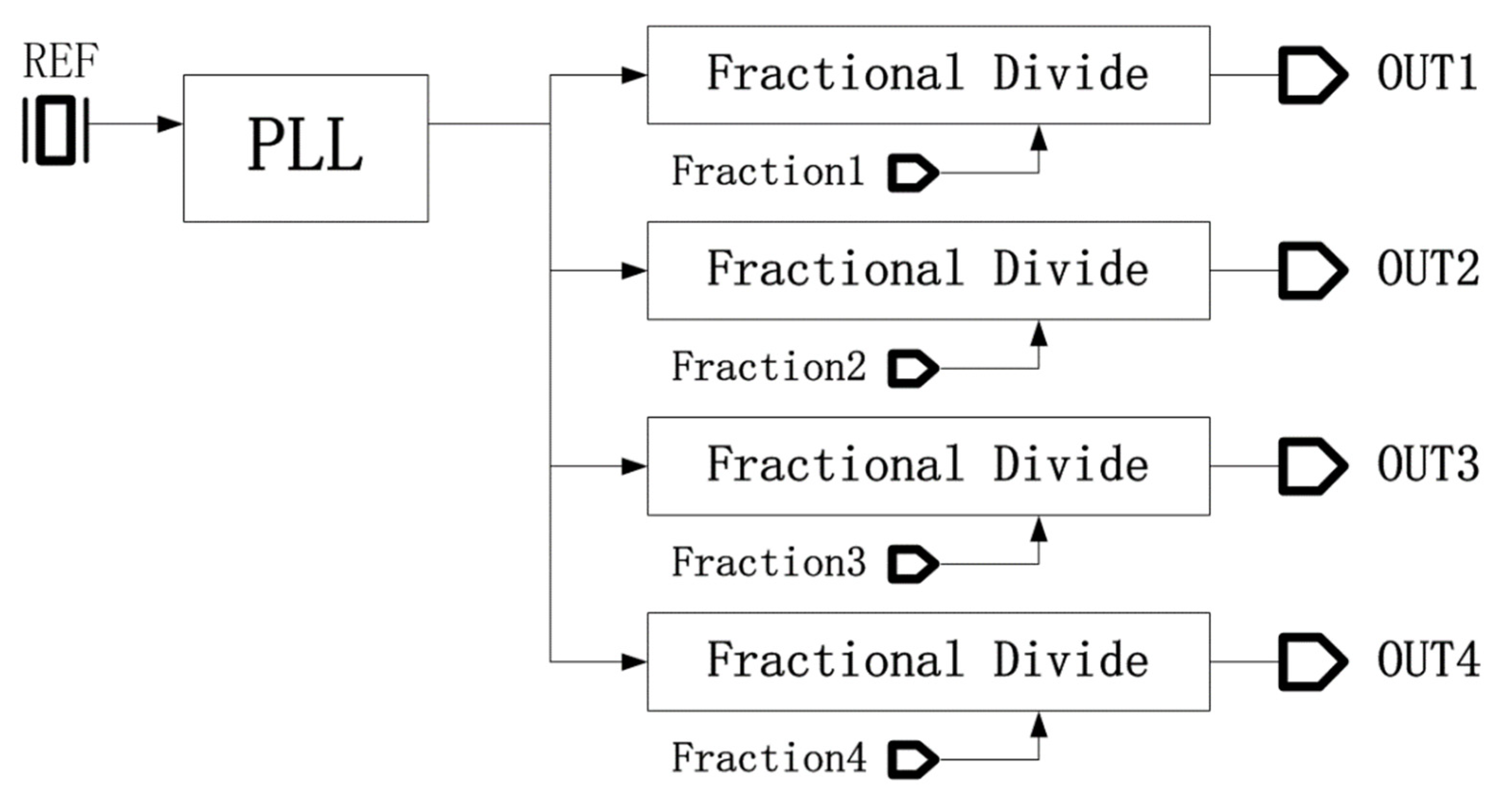
2. Materials and Methods
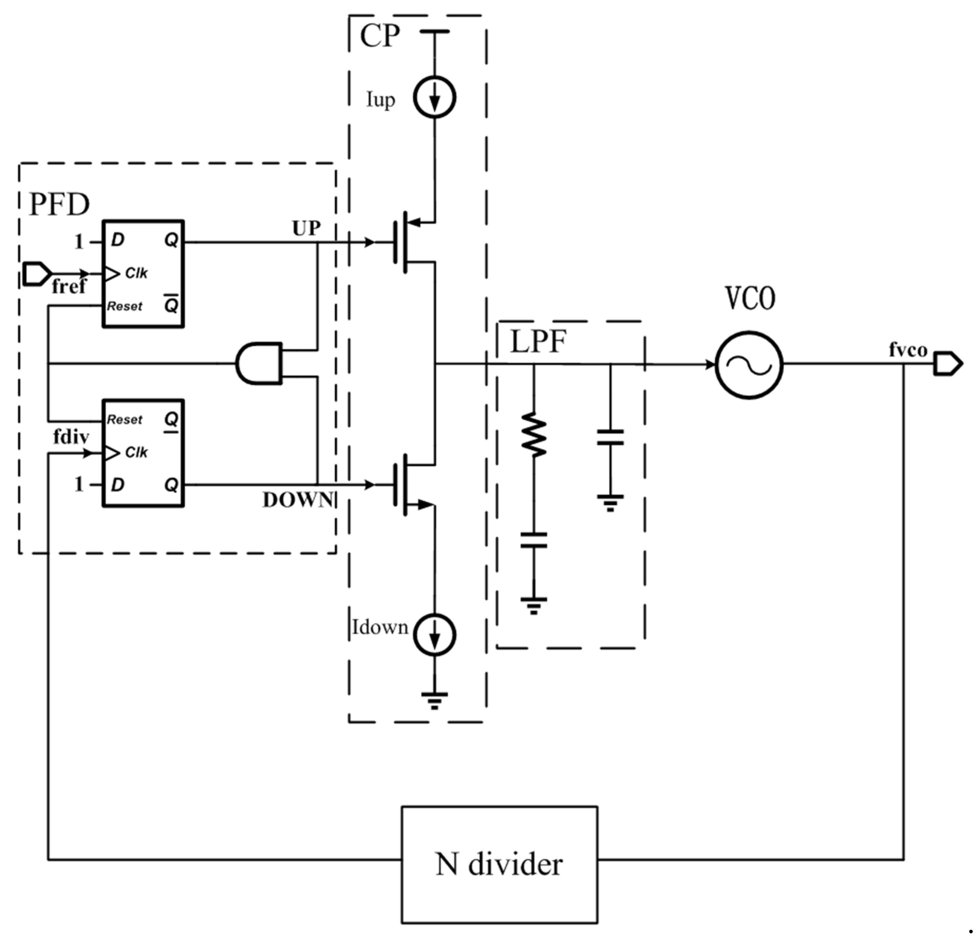
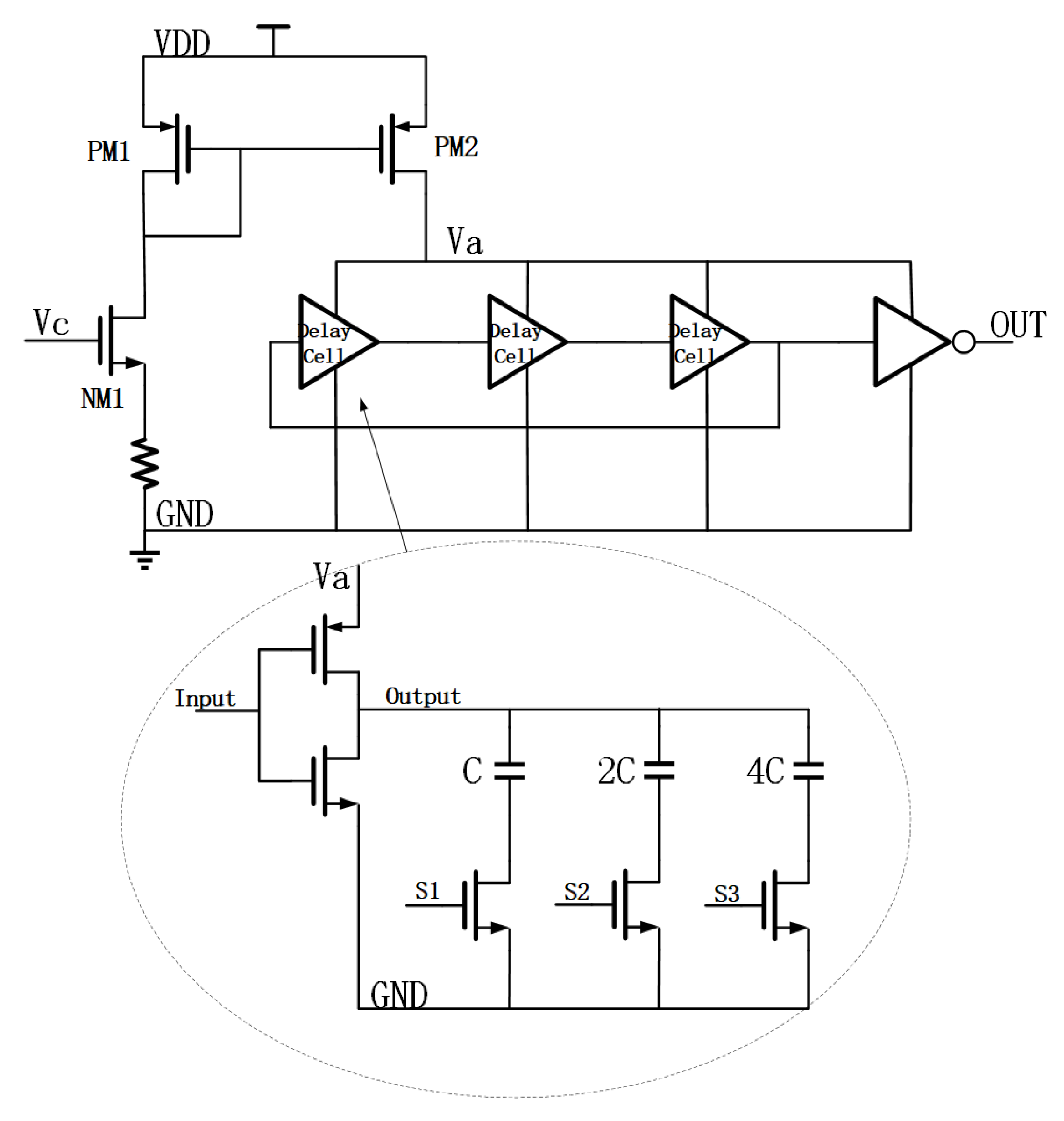
2.1. PLL Design
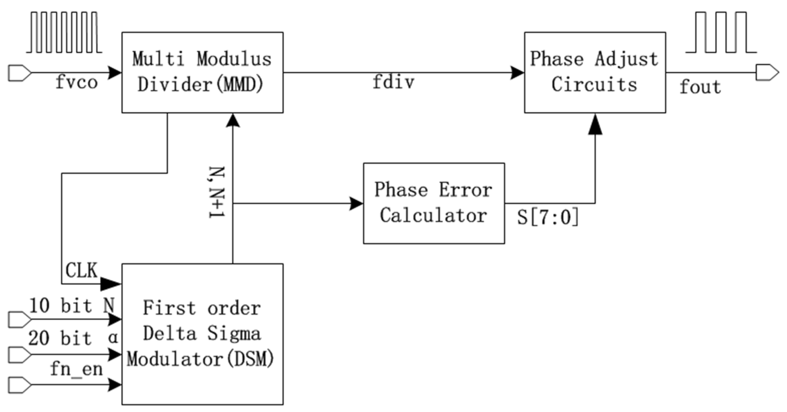
2.2. Open-Loop Fractional Divider Design
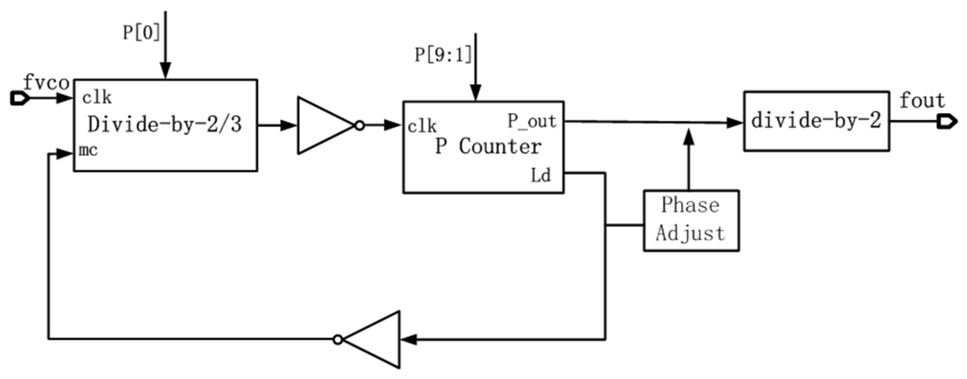
2.2.1. Multi-Modulus Divider
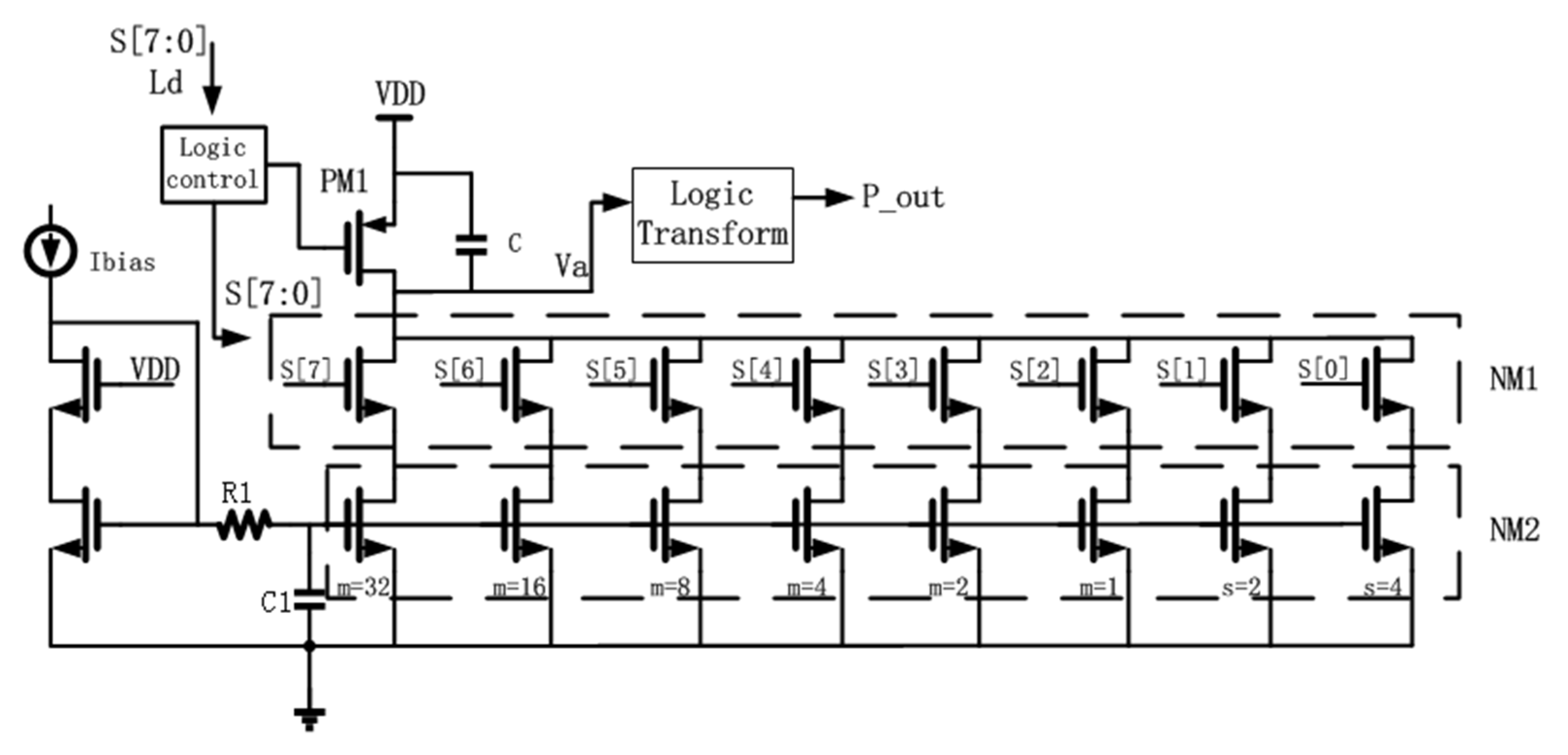
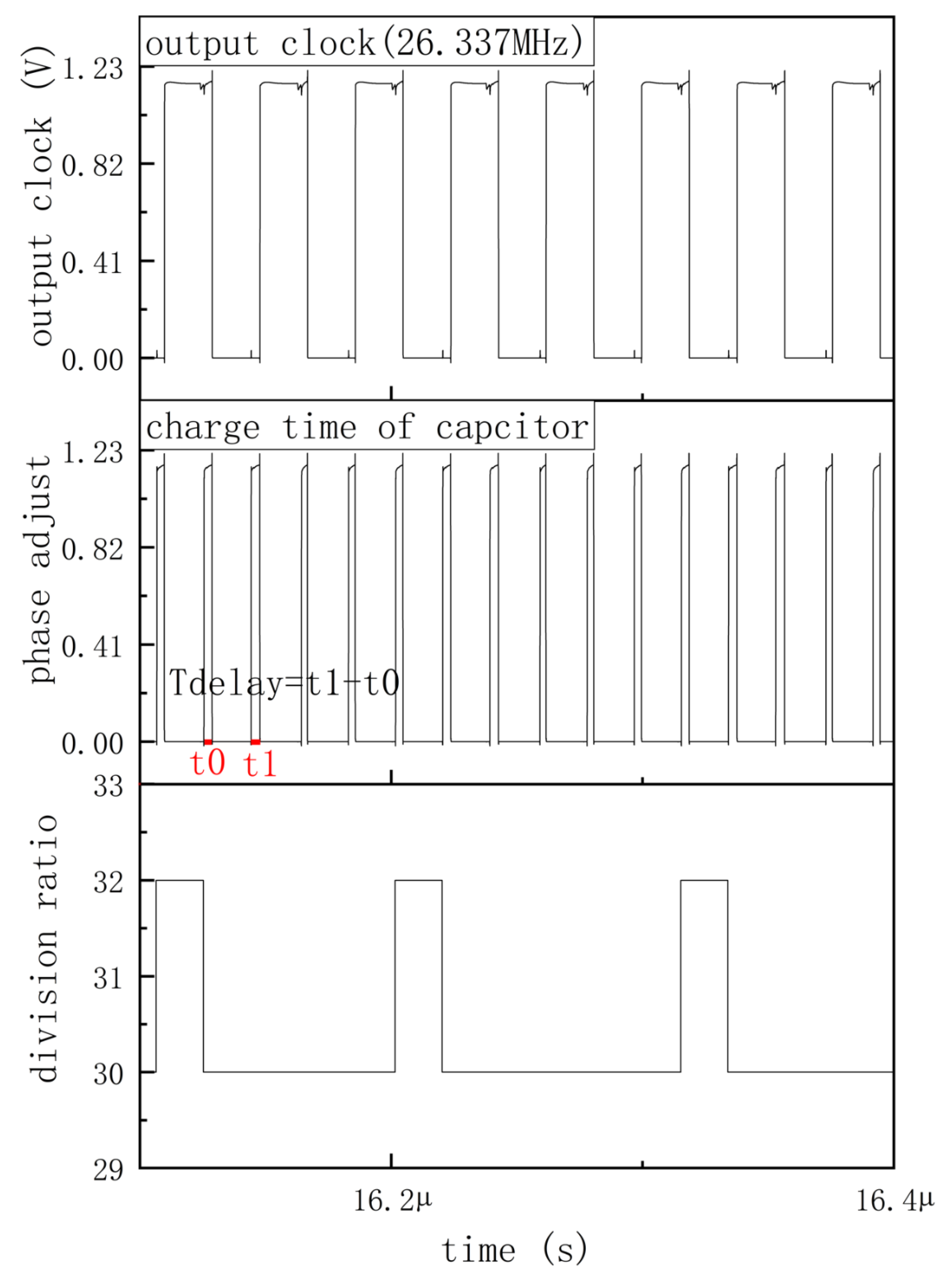
2.2.2. Phase-Adjusting Circuits
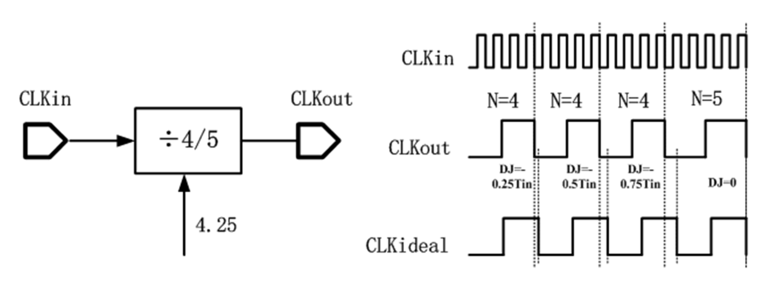
2.2.3. DSM and Phase Error Calculator
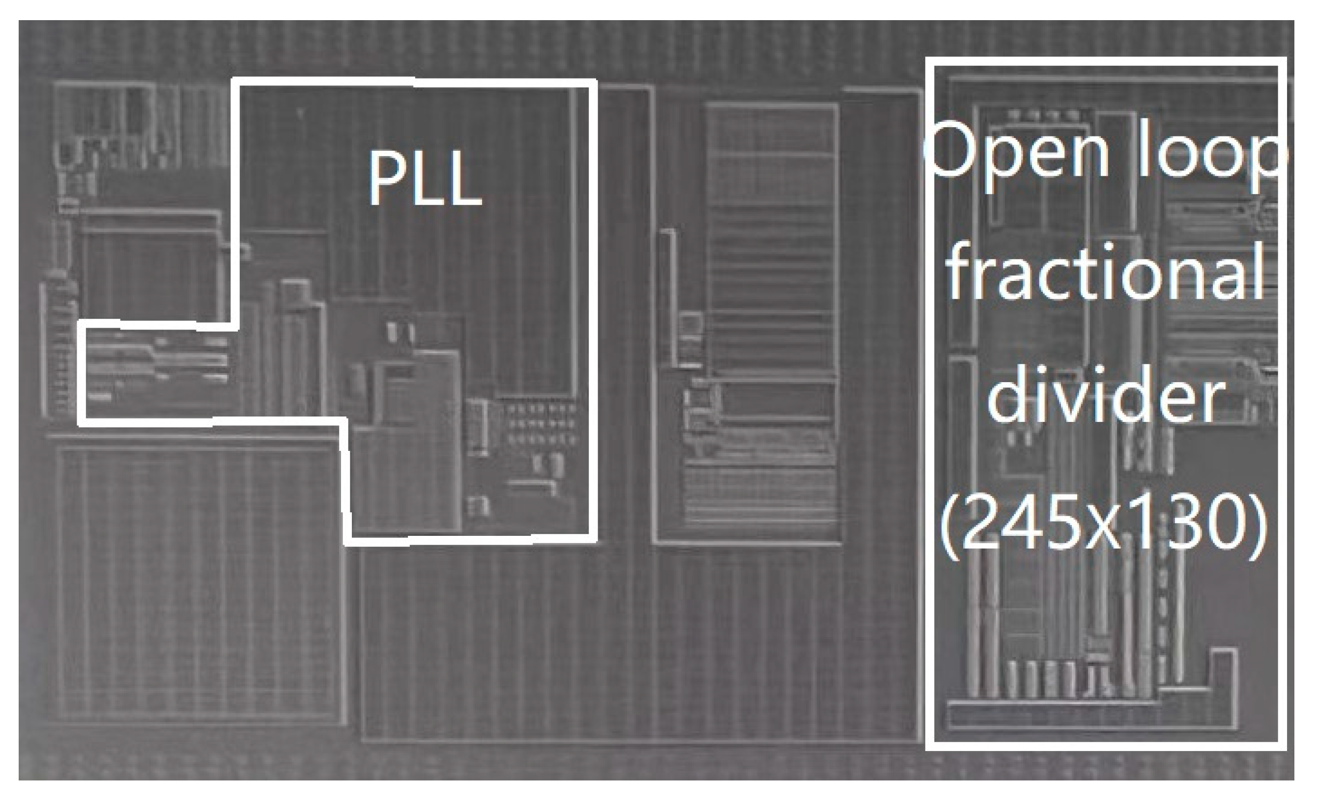
3. Results
3.1. Simulation Results
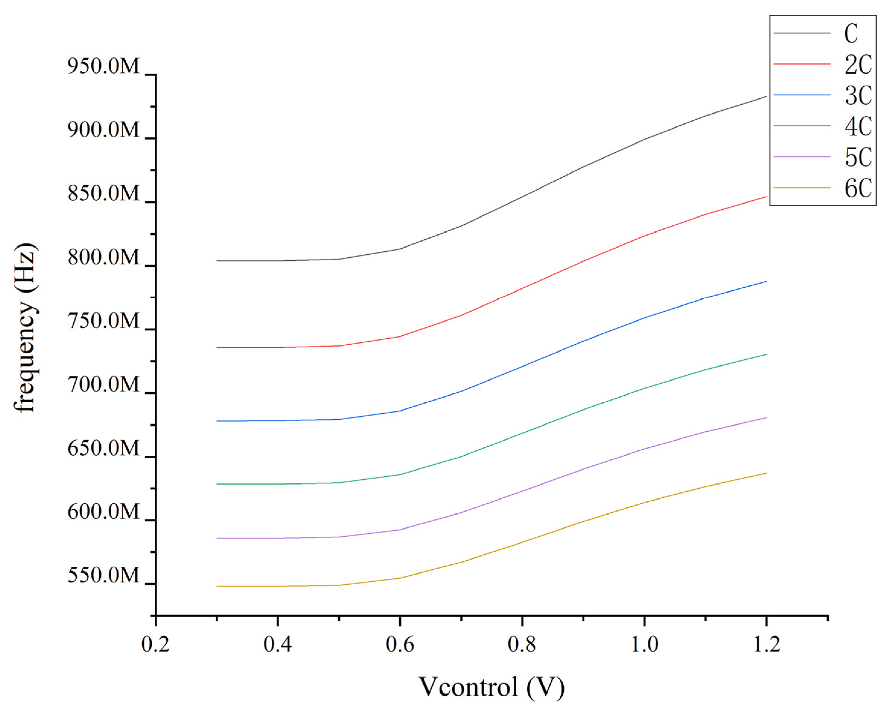
3.1.1. Tuning Range of VCO
3.1.2. Whole Performance
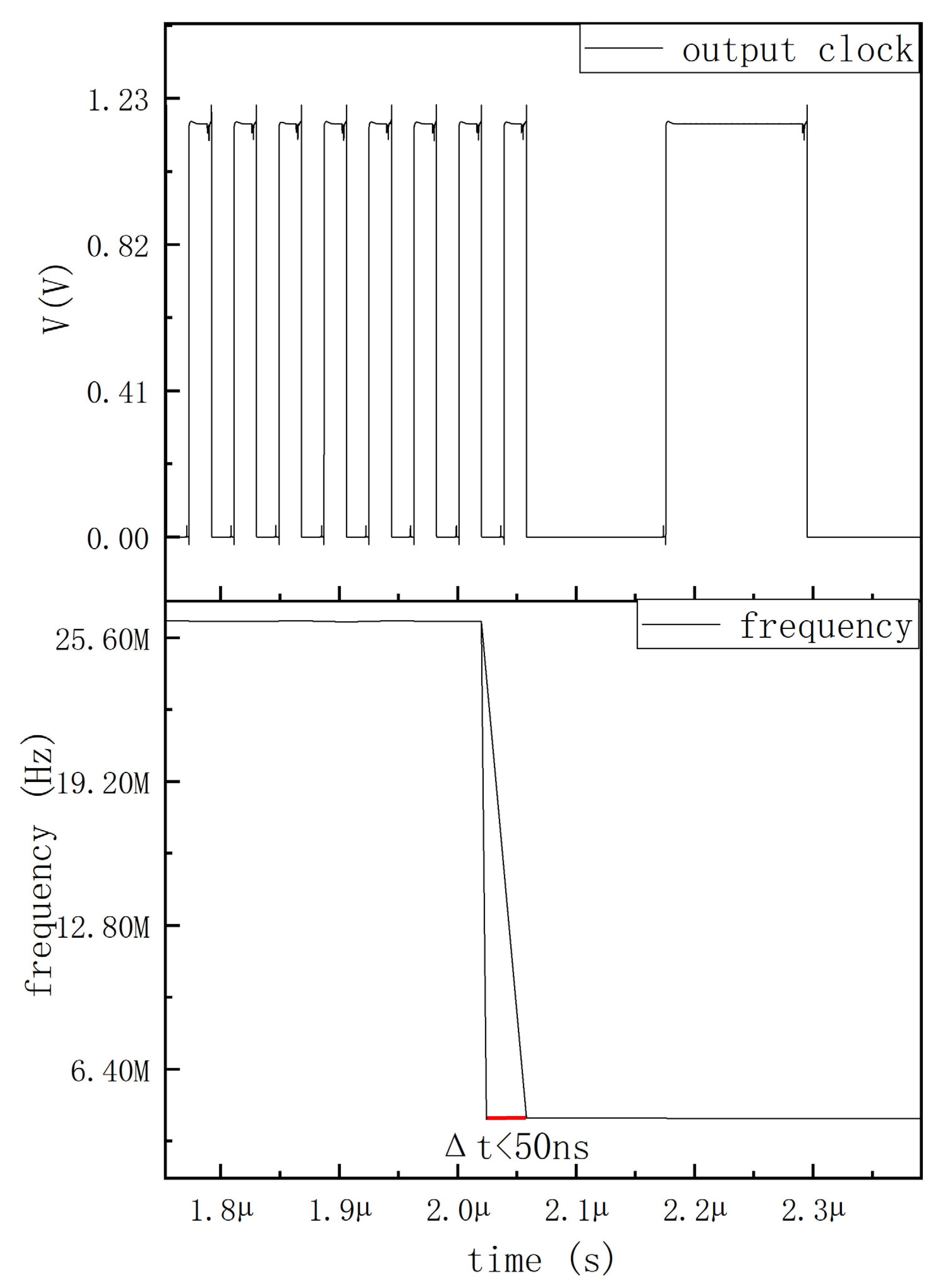
3.1.3. Frequency Switching Speed of Open-Loop Fractional Divider
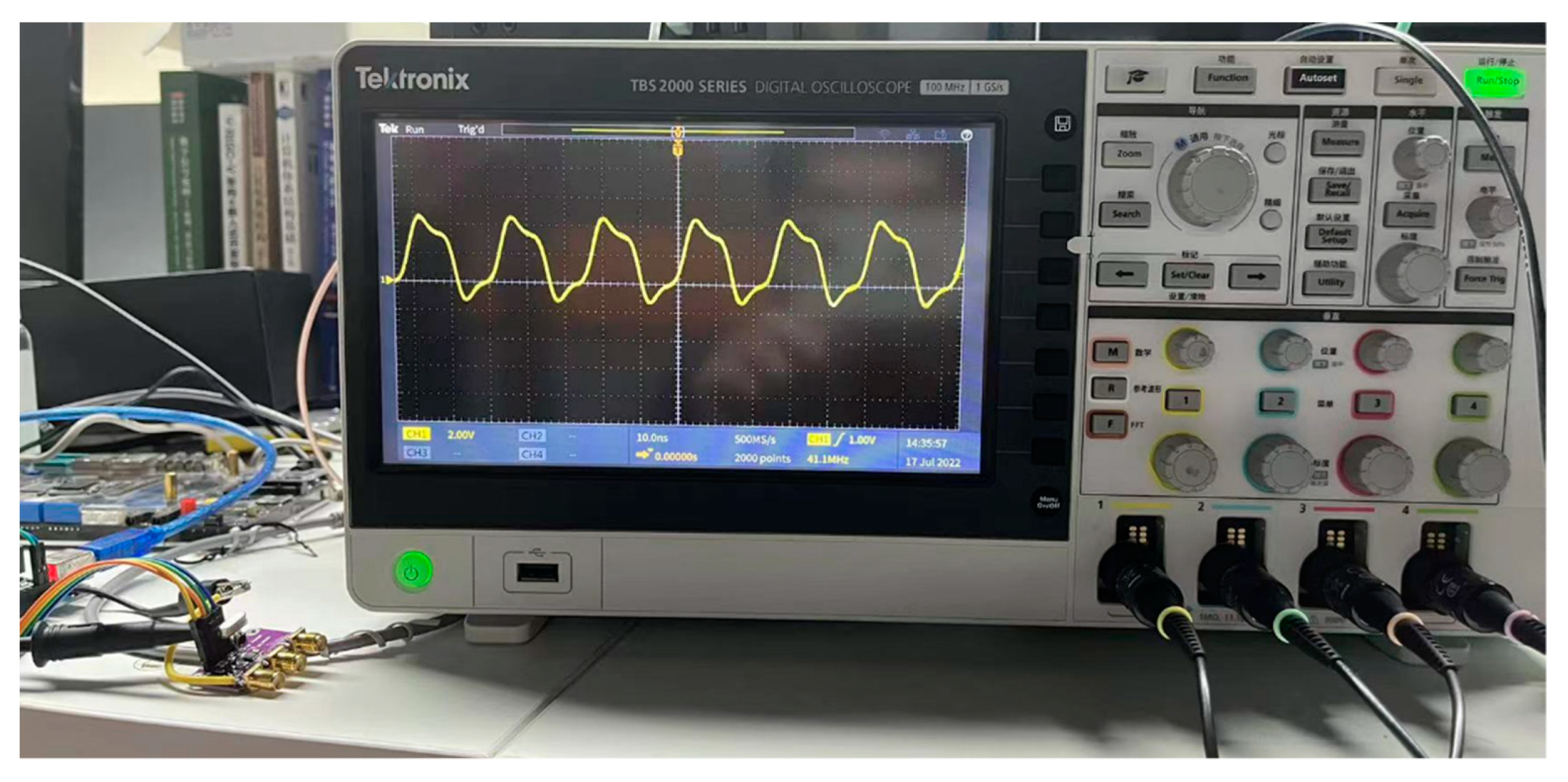
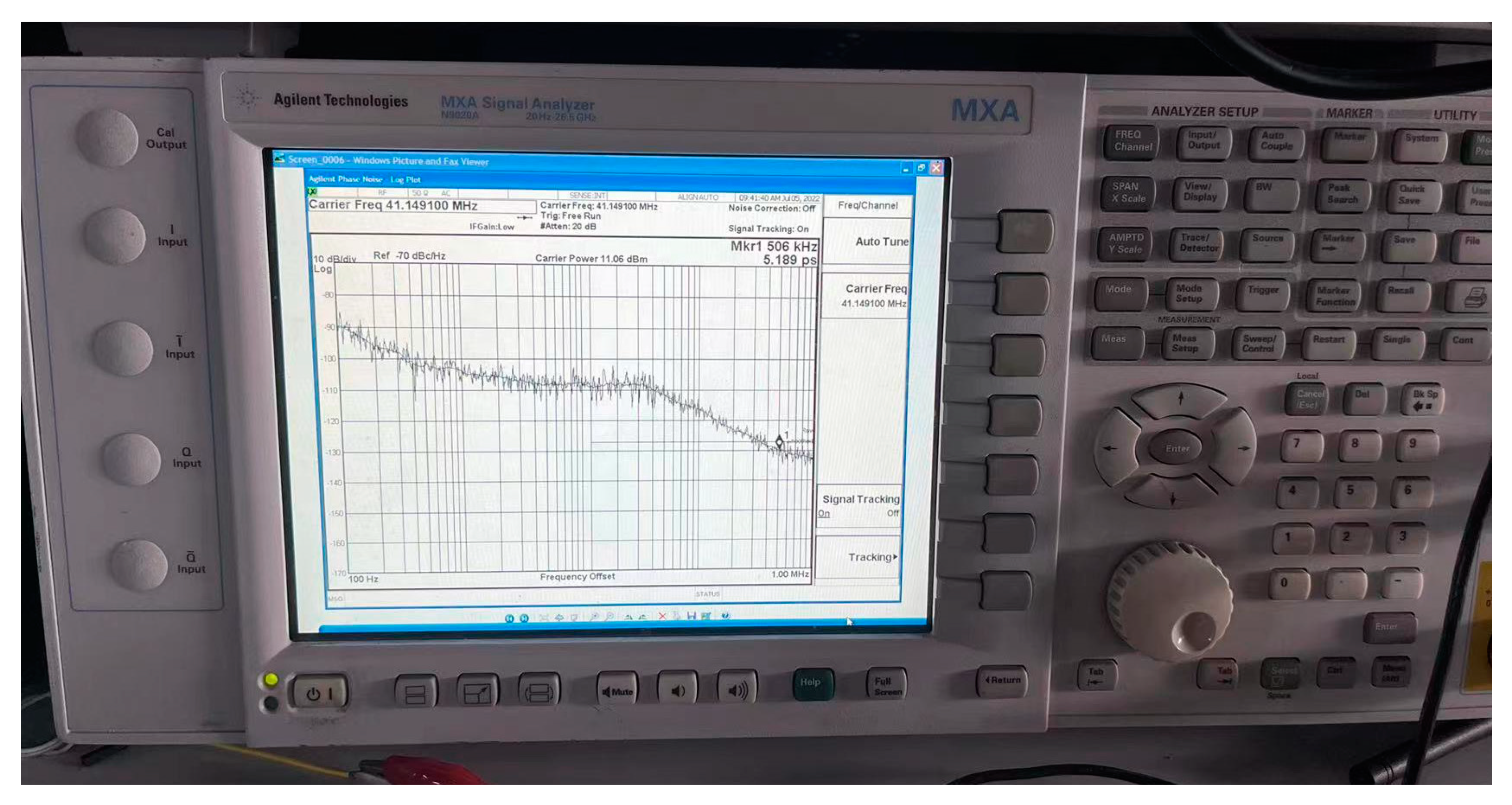
3.2. Test Results
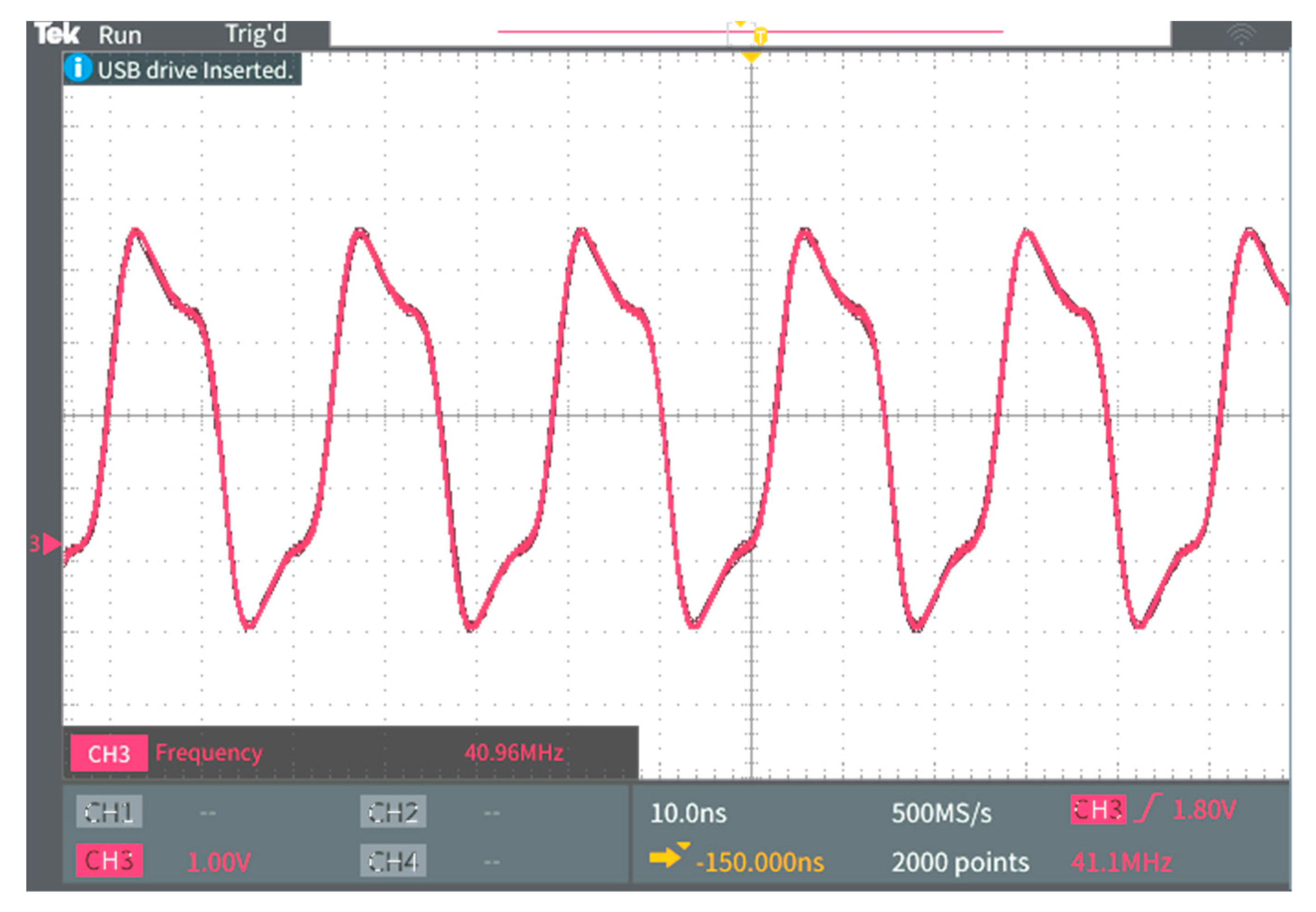
3.2.1. Output Clock
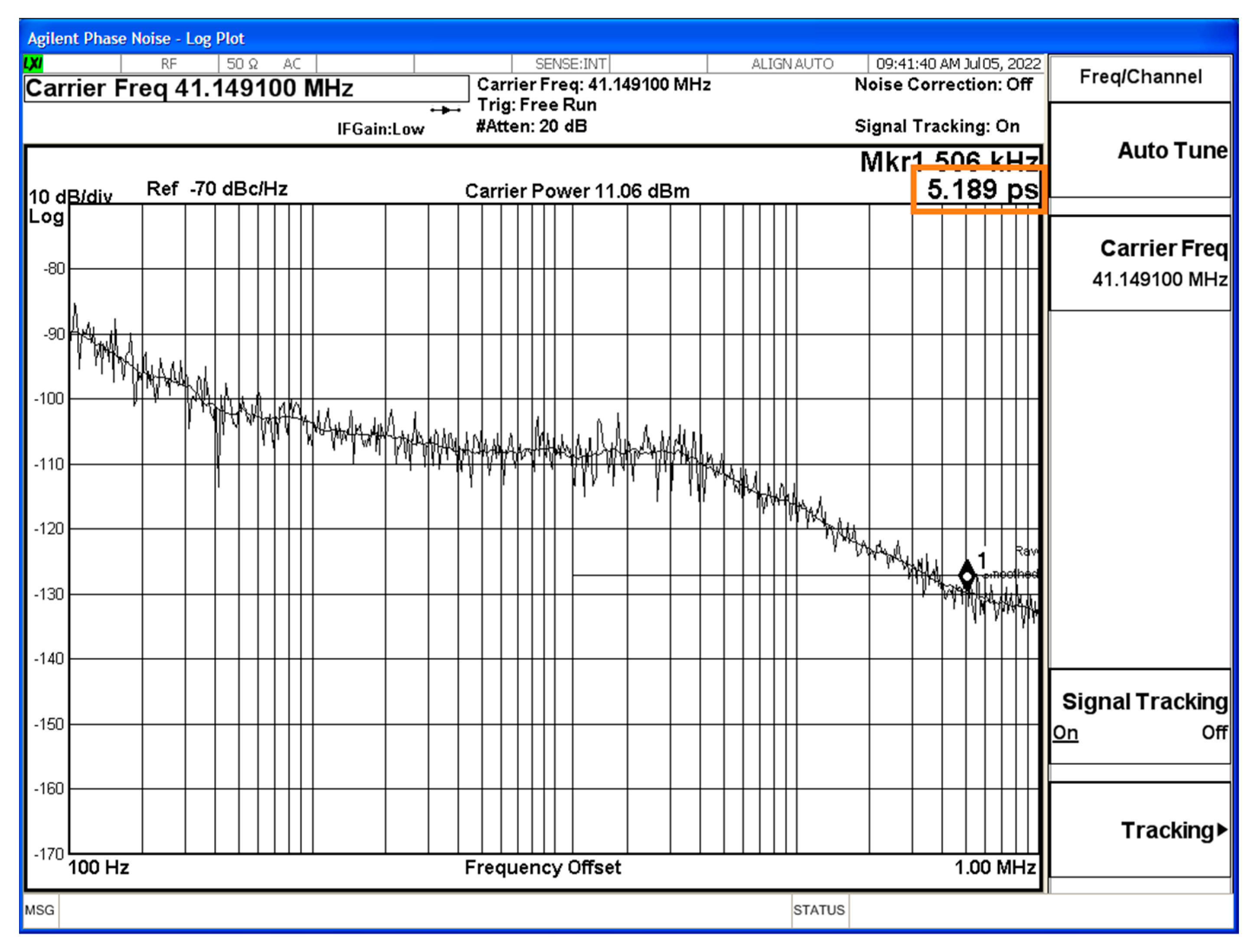
3.2.2. RMS Jitter
4. Discussion
5. Conclusions
Author Contributions
Funding
Institutional Review Board Statement
Informed Consent Statement
Data Availability Statement
Conflicts of Interest
Appendix A


References
- Kim, J.H.; Kwak, Y.H.; Kim, M.; Kim, S.W.; Kim, C. A 120-MHz–1.8-GHz CMOS DLL-Based Clock Generator for Dynamic Frequency Scaling. IEEE J. Solid-State Circuits 2006, 41, 2077–2082. [Google Scholar] [CrossRef]
- Hwang, J.; Jeong, G.S.; Chu, S.H.; Kim, W.; Jeong, D.K. A Crystal-Less Programmable Clock Generator with RC-LC Hybrid Oscillator for GHz Applications in 14 nm FinFET CMOS. In Proceedings of the BCICTS, San Diego, CA, USA, 15–17 October 2018. [Google Scholar]
- Fan, Y.; Guo, H.; Wang, R.; Zhang, Z.; Liao, H. A low-power calibration-free fractional-N digital PLL with high linear phase interpolator. In Proceedings of the 2016 IEEE Asian Solid-State Circuits Conference (A-SSCC), Toyama, Japan, 7–9 November 2016. [Google Scholar]
- Jamali, M.; Ebrahimi, E. A new Fractional-N frequency synthesizer using Nested-PLL architecture. In Proceedings of the Electrical Engineering, Tehran, Iran, 2–4 May 2017. [Google Scholar]
- Mahmoud, A.; Andreani, P.; Ping, L. A 65nm CMOS fraction-N digital PLL with shaped in-band phase noise. In Proceedings of the Nordic Circuits and Systems Conference (NORCAS): NORCHIP & International Symposium on System-on-Chip (SoC), 2015, Oslo, Norway, 26–28 October 2015. [Google Scholar]
- Allen, A.; Desai, J.; Verdico, F.; Anderson, F.; Mulvihill, D.; Dan, K. Dynamic frequency-switching clock system on a quad-core Itanium® processor. In Proceedings of the IEEE International Solid-State Circuits Conference-Digest of Technical Papers, San Francisco, CA, USA, 8–12 February 2009. [Google Scholar]
- Tierno, J.; Rylyakov, A.; Friedman, D.; Chen, A.; Stawiasz, K. A DPLL-based per core variable frequency clock generator for an eight-core POWER7 microprocessor. In Proceedings of the VLSI Circuits (VLSIC), 2010 IEEE Symposium on, Honolulu, HI, USA, 16–18 June 2010. [Google Scholar]
- De Caro, D.; Tessitore, F.; Vai, G.; Imperato, N.; Petra, N.; Napoli, E.; Parrella, C.; Strollo, A.G.M. A 3.3 GHz Spread-Spectrum Clock Generator Supporting Discontinuous Frequency Modulations in 28 nm CMOS. IEEE J. Solid-State Circuits 2015, 50, 2074–2089. [Google Scholar] [CrossRef]
- Elkholy, A.; Saxena, S.; Shu, G.; Elshazly, A.; Hanumolu, P.K. Low-Jitter Multi-Output All-Digital Clock Generator Using DTC-Based Open Loop Fractional Dividers. IEEE J. Solid-State Circuits 2018, 53, 1806–1817. [Google Scholar] [CrossRef]
- Suman, S.; Sharma, K.G.; Ghosh, P.K. Analysis and Design of Current Starved Ring VCO. In Proceedings of the International Conference on Electrical, Electronics, and Optimization Techniques (ICEEOT)-2016, Mysuru, India, 9–10 December 2016. [Google Scholar]
- Mishra, A.; Sharma, G.K.; Boolchandani, D. Performance analysis of power optimal PLL design using five-stage CS-VCO in 180nm. In Proceedings of the International Conference on Signal Propagation & Computer Technology, Ajmer, India, 12–13 July 2014. [Google Scholar]
- Blasco, G.; Isern, E.; Martin, E. Design of a stable pulse generator system based on a Ring-VCO Phase-Locked Loop using 180nm CMOS technology. In Proceedings of the Design of Circuits & Integrated Systems, Estoril, Portugal, 25–27 November 2016. [Google Scholar]
- Elkholy, A.; Saxena, S.; Nandwana, R.K.; Elshazly, A.; Hanumolu, P.K. A 2.0–5.5 GHz Wide Bandwidth Ring-Based Digital Fractional-N PLL With Extended Range Multi-Modulus Divider. IEEE J. Solid-State Circuits 2016, 51, 1771–1784. [Google Scholar] [CrossRef]
- Riley, T.A.D.; Copeland, M.A. Delta-sigma modulation in fractional-N frequency synthesis. IEEE J. Solid-State Circuits 1993, 28, 553–559. [Google Scholar] [CrossRef] [Green Version]
- Xu, X.; Rhee, W.; Wang, Z. A Low-Spur Current-Biasing-Free Fractional-N Hybrid PLL for Low-Voltage Clock Generation. In Proceedings of the 2020 IEEE International Symposium on Circuits and Systems (ISCAS), Seville, Spain, 12–14 October 2020. [Google Scholar]
- De Caro, D.; Romani, C.A.; Petra, N.; Strollo, A.G.M.; Parrella, C. A 1.27 GHz, All-Digital Spread Spectrum Clock Generator/Synthesizer in 65 nm CMOS. IEEE J. Solid-State Circuits 2010, 45, 1048–1060. [Google Scholar] [CrossRef]
- Ho, Y.-H.; Yao, C.-Y. A Fast-Acquisition All-Digital Delay-Locked Loop Using a Starting-Bit Prediction Algorithm for the Successive-Approximation Register. IEEE Trans. Very Large Scale Integr. (VLSI) Syst. 2016, 24, 759–763. [Google Scholar] [CrossRef]
- Elkholy, A.; Elshazly, A.; Saxena, S.; Shu, G.; Hanumolu, P.K. A 20-to-1000MHz±14ps peak-to-peak jitter reconfigurable multi-output all-digital clock generator using open-loop fractional dividers in 65nm CMOS. In Proceedings of the Solid-State Circuits Conference Digest of Technical Papers (ISSCC), 2014 IEEE International, San Francisco, CA, USA, 9–13 February 2014. [Google Scholar]


| [9] | [15] | [16] | [17] | This Work 1 | |
|---|---|---|---|---|---|
| Architecture | Fractional-N divider (DTC) | Fractional-N PLL | Fractional-N divider (DCDL) | Delay-locked loop (DCDL) | Fractional-N divider (analog phase-adjusting cell) |
| Technology (nm) | 65 | 65 | 65 | 180 | 130 |
| Supply (V) | 0.9 | 0.65 | 1.2 | 1.8 | 1.2 |
| Input frequency (MHz) | 5000 | 60 | 1270 | NA | 600–900 |
| Output frequency (MHz) | 20–1000 | 1000–1500 | 180–1270 | 60–1100 | 0.5–150 |
| RMS jitter (ps) | 1.44 | 14.0 | 12.8 | 1.4 | 5.2 |
| Instantaneous switching | Yes | No | Yes | No | Yes |
| Power consumption | 3.2 mW | 1.85 mW | 19.8 mW | 23 mW | 7.7 mW |
| Area (mm2) | 0.017 | 0.23 | 0.044 | 0.066 | 0.032 |
Publisher’s Note: MDPI stays neutral with regard to jurisdictional claims in published maps and institutional affiliations. |
© 2022 by the authors. Licensee MDPI, Basel, Switzerland. This article is an open access article distributed under the terms and conditions of the Creative Commons Attribution (CC BY) license (https://creativecommons.org/licenses/by/4.0/).
Share and Cite
Jin, J.; Jin, Y.; Gan, Y. A 500 kHz to 150 MHz Multi-Output Clock Generator Using Analog PLL and Open-Loop Fractional Divider with 0.13 μm CMOS. Electronics 2022, 11, 2347. https://doi.org/10.3390/electronics11152347
Jin J, Jin Y, Gan Y. A 500 kHz to 150 MHz Multi-Output Clock Generator Using Analog PLL and Open-Loop Fractional Divider with 0.13 μm CMOS. Electronics. 2022; 11(15):2347. https://doi.org/10.3390/electronics11152347
Chicago/Turabian StyleJin, Junting, Yuhua Jin, and Yebing Gan. 2022. "A 500 kHz to 150 MHz Multi-Output Clock Generator Using Analog PLL and Open-Loop Fractional Divider with 0.13 μm CMOS" Electronics 11, no. 15: 2347. https://doi.org/10.3390/electronics11152347