1. Introduction
Nowadays, the development of renewable power sources is driving interest towards DC–DC converters in particular for their control. Indeed, the majority of these sources are characterized by a low voltage output, i.e., photovoltaic panels, fuel cells, etc, as well as the majority of storage systems, i.e., batteries, supercapacitors, etc. This means that a DC–DC conversion stage is needed in order to allow the distribution of such energy [
1]. For this reason, a relevant effort has been made to increase both the efficiency of DC–DC converters and their steady-state gain. The improvement of efficiency of this kind of system is important because it reduces the energy losses caused by switching and by the Joule effect. The steady-state gain is also relevant in terms of reducing the number of conversion stages when a high conversion ratio is required. A converter particularly suitable for the above-mentioned applications is the Quadratic Boost Converter (QBC), since it presents a high voltage ratio. Among the existing configurations of these converters, it is possible to distinguish two main topologies. The first one consists in two independent boost stages with two switching devices [
2], while the second one is composed of a single conversion stage with only one switching device [
3]. In this paper, attention is focused on this last configuration, since the switching losses are reduced, allowing to potentially obtain a higher efficiency.
Among the control techniques proposed in the literature, sliding mode control is widespread, especially regarding single stage boost converters. For example, in [
4] a sliding mode control law is designed for a boost converter according to a chosen sliding function. The implementation of this sliding mode controller leads to a converter control method with variable frequency. Since in practical applications it is requested that the converter is driven according to the PWM control method, the authors describe a conversion method from variable frequency control to a PWM control. The method is based on the interpretation of the equivalent control associated with the switching surface, as the duty cycle of the PWM control method. In [
5], a robust sliding mode control law is proposed and experimentally tested for a boost converter. The robustness is achieved by means of an adaptive scheme which adjusts the parameters in order to cope with the variations of the load resistance and input voltage. The implementation of the controller is carried out as in [
4], i.e., determining the equivalent control and using it as a duty cycle. In [
6], a controller is proposed, consisting of an outer loop PI-type which gives the reference current, and a sliding mode inner control loop for the tracking of the reference current itself, using the tracking current error as sliding function. The implementation of the controller is carried out on a microprocessor-based device, and this allows the implementation of a predictive conversion strategy from the sliding mode control law to PWM control of the converter. In [
7], a total sliding-mode Lyapunov-based control scheme is designed to ensure stable tracking performance under system uncertainties. There are also works that propose different interpretations of the sliding mode control for boost converters. For example, in [
8] a sliding mode control technique is proposed for switched affine models, characterized by a continuous set of equilibrium states. The sliding function is obtained using an extended linearization method [
9]. Simulation experiments show the peculiarities of the followed approach. In [
10], a control technique is proposed for the same class of models, based on the minimization of an upper bound quadratic cost function involving the difference of the actual state and the desired equilibrium state. In [
11], it is shown that the control strategy proposed in [
8] is equivalent to a sliding mode strategy along a particular sliding surface, designed by means of a min-type algorithm.
With regard to quadratic boost converter, Refs. [
12,
13] propose a controller consisting of two control loops. In [
12], the outer PI-type control loop regulates the output voltage, and gives the inductor reference current for the inner current loop. The inner control loop is designed using the low signal model corresponding to the averaged state space model. The control methodology used is the classical one in the frequency domain. In [
13], a PI compensator regulates the output voltage giving the reference current for the inner loop. The inner loop is based on the sliding mode control of the current in the input inductor of the converter. The outer loop is designed using the classical approach in the frequency domain. In [
14], a single quasi-resonant network that operates in a zero-current switching way is implemented with the aim of reducing the switching losses and obtain a higher conversion ratio. In [
15], a hybrid control based only on the measurements of the input and output voltages is proposed by encompassing a control law and an observer for the estimation of the system states and, in particular, the inductor currents. Finally, in [
16], starting from a hybrid model of the power converters, a PWM control algorithm is designed for the command of the converter, overcoming the well known approach based on the averaged state space model, having the duty cycle as input variable.
In this paper a sliding mode controller for a QBC is proposed but, differently from the papers [
4,
5,
6,
7], the sliding function is not based on the tracking errors of current or voltage, but it is more complex, depends on all the state variables, and is non-a priori defined, but it is derived from the design requirements and the employed control methods. Since the converter has to work in a wide range of equilibrium points, the sliding function is derived from the extended linearization approach [
8,
17]. Note that the sliding mode control of DC–DC power converters via extended linearization has been studied, from a theoretic point of view, in few cases in the literature regarding a standard boost converter (cf., for example, ref. [
17]) and a buck-boost power converter [
18,
19], but it has never been studied nor experimentally applied to a quadratic boost converter to the authors’ best knowledge. Moreover, another design requirement is the robustness of the controller against parametric uncertainties and load and input voltage variations, and for this reason an outer loop with integral-type controller is designed.
The extended linearization method represents a systematic procedure of sliding mode controller design, where a nonlinear sliding surface, with well-defined properties, is designed on the basis of an extension of a linear sliding control carried out for affine linear models of converters. An important property of the proposed approach arises in the fact that if there is a sudden change in the nominal operating conditions, the control system automatically stabilizes, by means of a new sliding regime, the system trajectories of the new equilibrium point. The main advantage of this procedure is that the resulting sliding dynamics can be made linear by means of a suitable state coordinate transformation derivable from the linearized system model. The starting point is the construction of a model linearized around the desired equilibrium state and, assuming that it is controllable, the system is put in the control canonical form by means of a coordinate transformation. A linear sliding surface is chosen for this canonical form and then transferred into a nonlinear sliding surface in the starting coordinate frame. Finally, the integral controller of the outer loop updates the equilibrium state in order to maintain the output error at zero in the presence of load and input voltage variations, and converter parametric uncertainties. The implementation of the control law previously described is carried out with a constant sampling frequency. This frequency is chosen as the maximum allowable for computing the control law, and it depends on the computational power of the digital signal processor (DSP), and the complexity of the control law. Differently from almost all the papers cited before, the proposed control is not PWM-type. Indeed, the controller, at each sampling interval, decides if a commutation is required. Consequently, the switching frequency results vary and are less than (or equal to) the sampling frequency.
The paper is organized as follows. Firstly, a physical model is considered starting from the QBC circuit layout where the parasitic resistances of the inductances are considered. Then, a discontinuous fourth-order switching input-state-output mathematical model is provided. Given the discontinuous nature of the mathematical model, an affine LTI system is associated with it, which allows to determine the equilibrium states. Subsequently, the dynamics matrix of this model can be put in the companion form by means of an auxiliary input gain vector, and the corresponding coordinate transformation is computed. Then, a suitable sliding surface given by a linear combination of the state variables is defined, so that during the sliding motion on this surface the system is described by a linear, stable and autonomous third-order model. Lastly, the final sliding surface is expressed in terms of the current coordinates, obtaining a nonlinear sliding surface in terms of the coordinates of the original discontinuous model. The integral controller is designed using frequency domain control techniques so that the input–output stability of the whole control system in assured with a sufficient margin. The proposed control strategy has been tested experimentally in a suitable developer test set up, showing good closed loop behaviour.
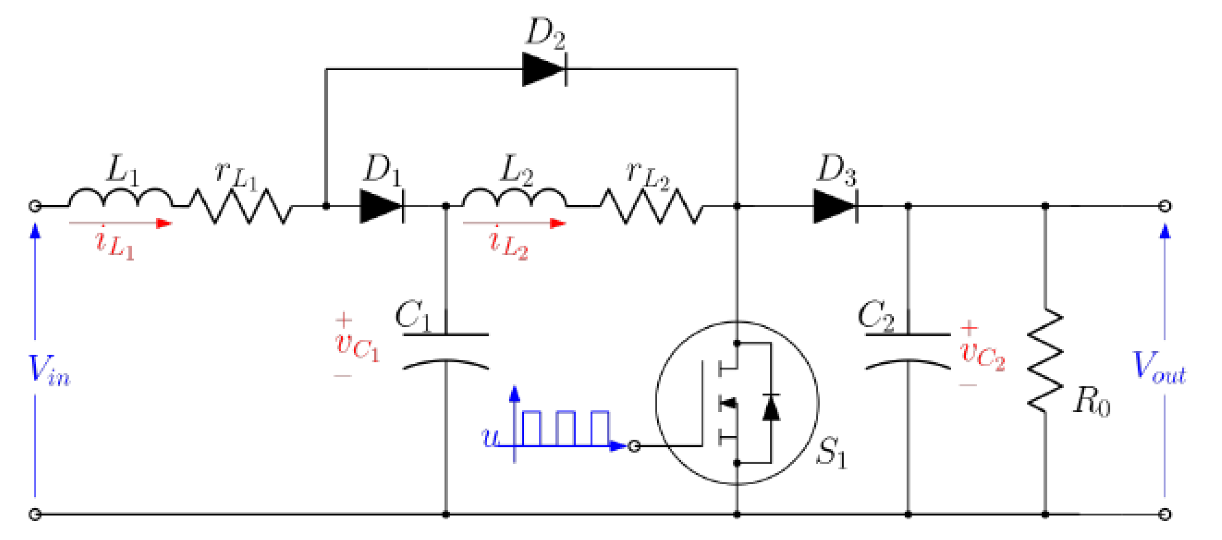
2. Dynamic Model of the Quadratic Boost Converter
The electrical circuit of the QBC considered in this paper is shown in
Figure 1. The converter can be modelled as a switching system consisting of a set of two models, defined by the status of the switch driving the converter itself, which is considered as an input and denoted by
. More precisely,
is associated with the status OFF, and
is associated with the status ON. Then, defining the state vector as follows:
the mathematical model of the QBC of
Figure 1 is given by:
where
is the input voltage,
y is the measured output and the matrices of the model are:
Models (
2) and (
3) make up a switching model consisting of two linear time invariant (LTI) models described by the dynamic matrices
when the status of the switch is OFF, and
when the status of the switch is ON. In both cases, the voltage
is assumed to be constant. It is easy to verify that, since the inductors’ parasitic resistances are taken into account, both models are asymptotically stable.
In the contest of the switching models, it is important to define appropriately the equilibrium states. This can be made associating the switching model with an affine averaged model as illustrated in [
8,
17,
20]. In particular, the affine averaged model, associated with (
2) and (
3), is given by:
where:
and lambda
. Note that matrix
is a convex combination of the matrices
and
, and it is a Hurwitz matrix for
. Note that models (
4) and (
5) coincide with models (
2) and (
3) when
(OFF state) and when
(ON state).
Model (
4) allows to determine the set of its equilibrium states
. This set is defined as:
whose explicit expression is given by:
where
.
It is useful to note that the determinant of
, given by:
is always greater than zero for all
and, consequently, there always exists an equilibrium point given by
. The output associated with
is
.
Before the presentation of the control strategy, it is useful to study the structural properties of models (
4) and (
5). With regard to the observability properties, the system is not observable for all functioning modes; indeed, when the switch is in ON mode the observability matrix rank is equal to 1; therefore, the system is not observable in this mode. Nevertheless, the QBC is observable when it works in OFF mode because the observability matrix presents full rank for any value of the parameters. Note that this problem is the same one observed for the standard boost case [
21] and it presents a physical interpretation. Indeed, it is easy to see in
Figure 1 that, when the converter works in ON mode there is no information about the inductor currents
and
and about the voltage
that are being inferred from the output. The same considerations can be obtained by studying the reachability property; indeed, by computing the rank of the reachability matrix, it is not full-rank when the converter works in ON mode, while it is full-rank when it is in OFF mode. For all other values of
different from 0 and 1,
, the model (
4) and (
5) results are both observable and reachable.
4. Experimental Set-Up
A test setup has been suitably built to validate the proposed control technique. The general architecture of the experimental set-up follows the schemes shown in
Figure 3.
The converter under test is shown in
Figure 1 and the parameters, as well as the used components, are given in
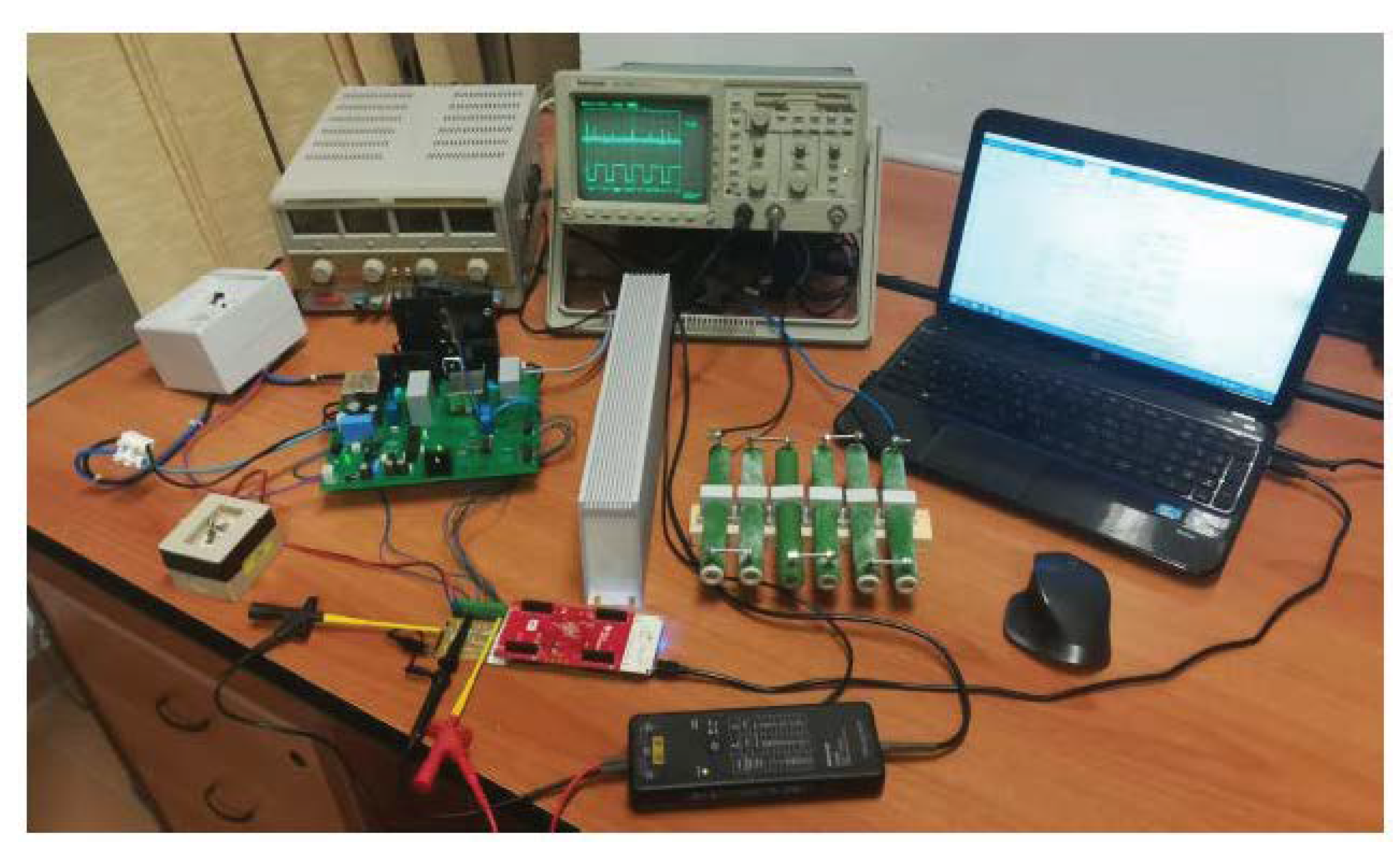
Table 1. A photo of the test bench is shown in
Figure 5.
The controller was digitally implemented using the C2000 32-bit TI microcontroller TMS320F28379D that has an additional built-in dedicated processor acting as the control law accelerator (CLA). In particular, the implementation is developed so that the SM algorithm runs in the dedicated CLA CPU while the main CPU takes account of other non-real-time tasks. Due to the variable frequency nature of the control law, the digital controller was implemented by directly driving the DSP digital output connected to the switch instead of using a PWM module that runs at a fixed frequency. To accomplish this task, the peculiar architecture of the TMS320F28379D was exploited. In particular, the control law was executed on the CLA (control law Accelerator), which takes 3.125 s to execute the ADC conversion and to evaluate whether a change in the digital output must be imposed. This time can be interpreted as a dwell time for the commutation. With this implementation strategy, the maximum achievable frequency results in 320 kHz. In any case, this does not mean that the switching frequency is always the maximum; indeed, if the SM control strategy does not need to impose a change in the state of the switch, no transactions are imposed on the DSP digital pin, thus resulting in a switching frequency lower than the maximum one of 320 kHz.
The inductor currents and are measured by means of Hall-effect sensors LEM LTS-15-NP, while the and voltages are measured by means of a voltage divider and an operational amplifier LM324 in buffer configuration. All signals are sampled and converted by the four embedded analogues to digital converters and processed by the microcontroller.
5. Experimental Results
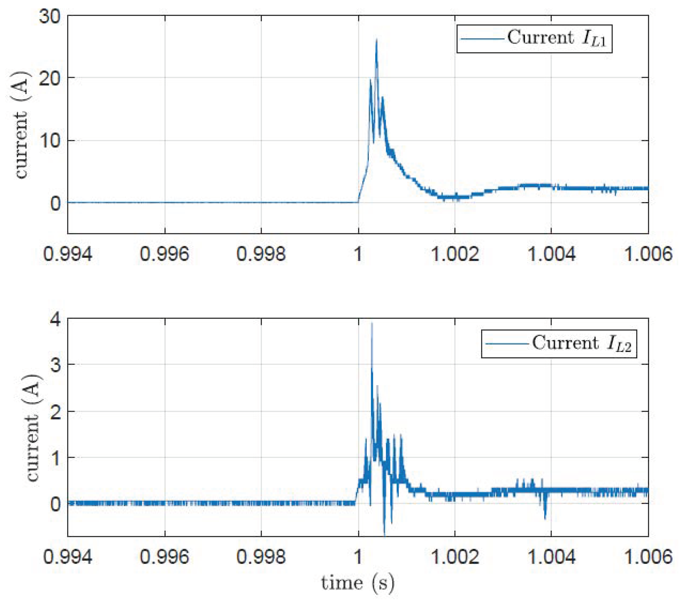
In this section, experimental results are given. In particular, a start-up test, a load variation test and a supply voltage variation test were carried out to validate the effectiveness of the proposed controller.
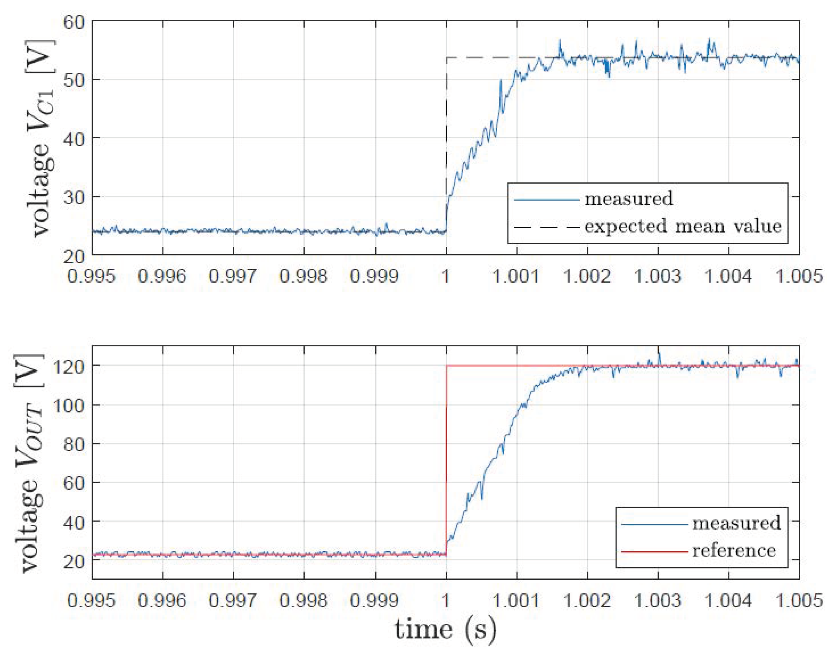
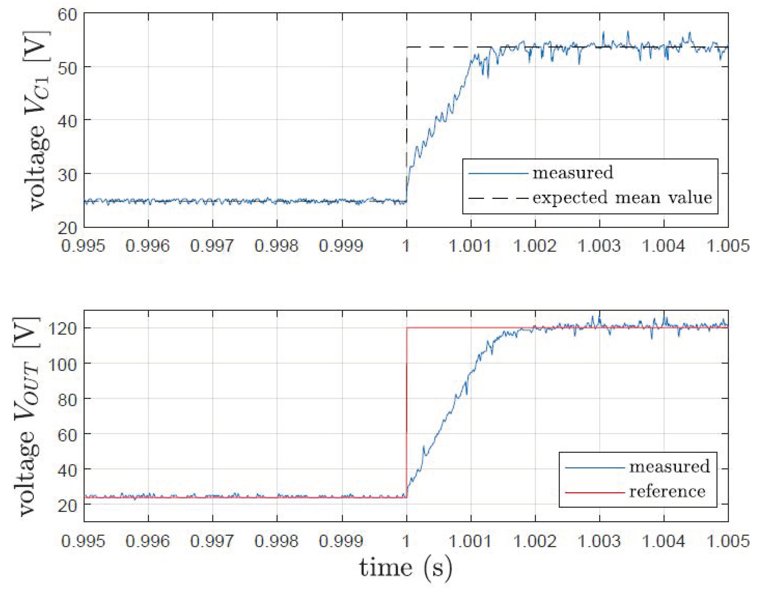
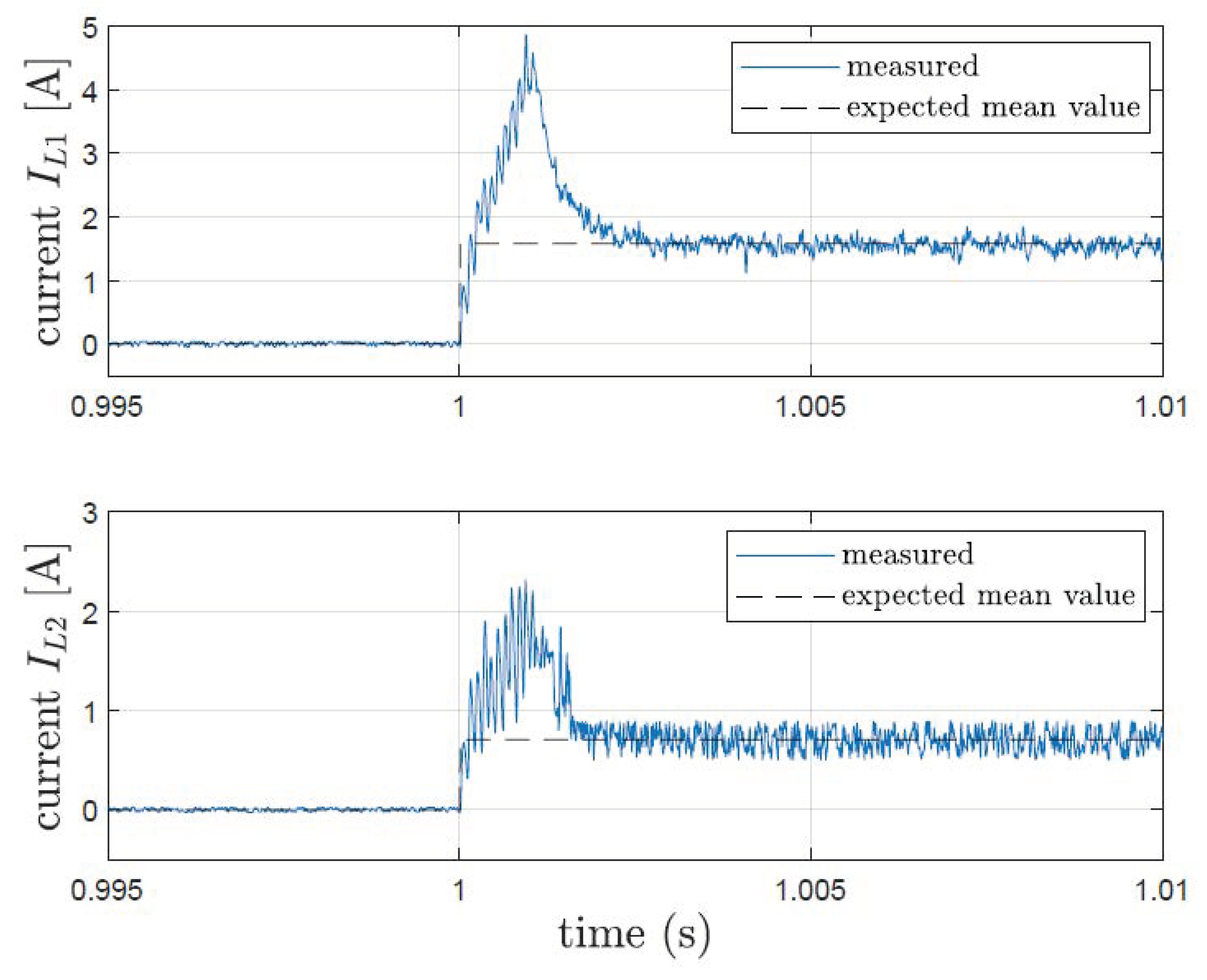
Figure 6,
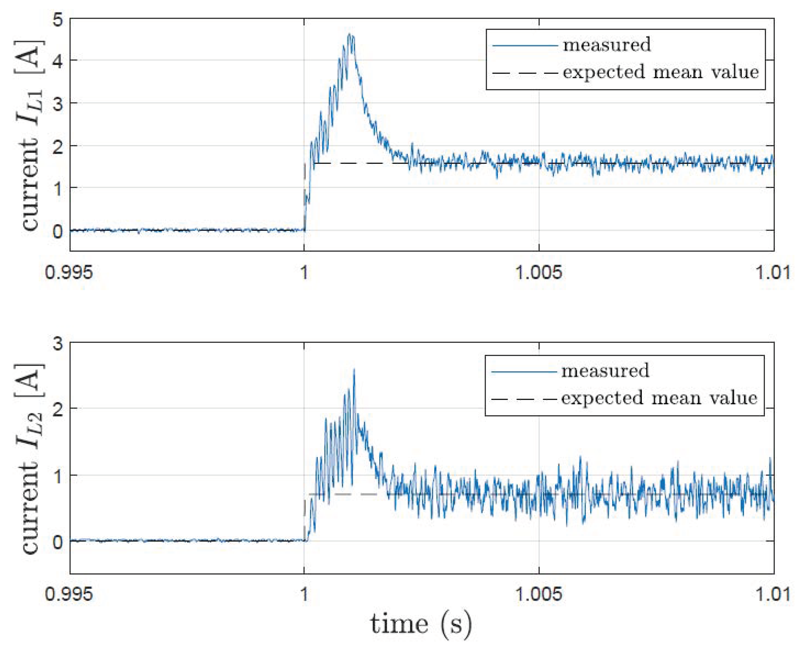
Figure 7 and
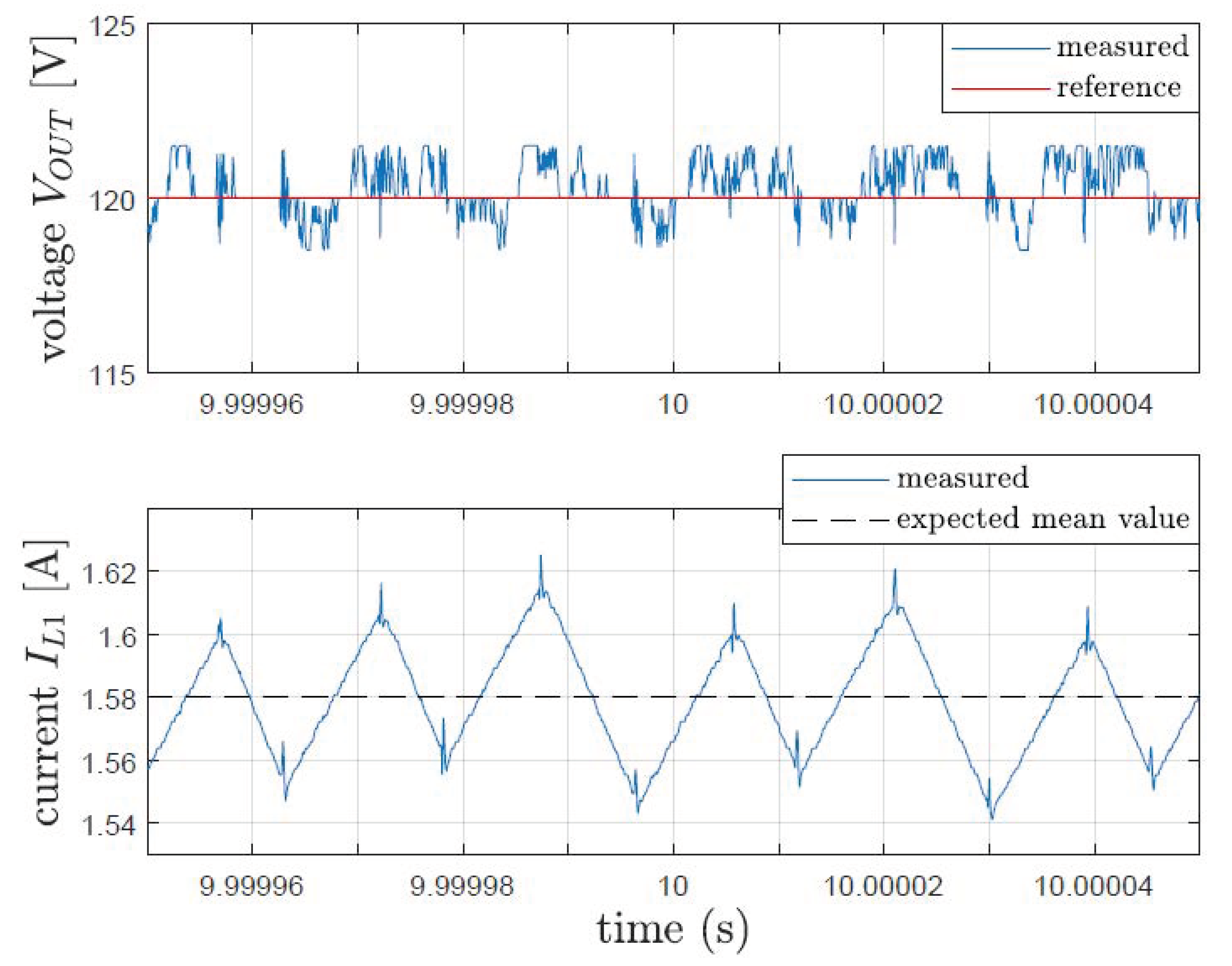
Figure 8 are relative to the behavior of the system with the proposed control scheme of
Figure 3 without the outer loop. In particular,
Figure 6 shows
and
voltages,
Figure 7 shows the waveforms of the inductor currents
and
, while
Figure 8 shows the behaviour of the converter at the steady state. From these figures, it is evident that the converter behaves very well; indeed, the current and voltage waveforms reach their steady-state values very fast (about 2 ms), with almost null voltage overshoot and a very limited inrush current. These current overshoots are due to the fact that the output capacitor is discharged at the beginning of the experiments. For this reason, in order to obtain a fast output voltage response a high current is required. In any case, the current is limited and well tolerated by the converter. This confirms the expected results. In particular, the proposed algorithm allows one to control all the state variables (instead of the output variable only), exhibiting an instantaneous control action. Moreover, from
Figure 8, it is possible to appreciate a good voltage regulation at a steady state, with small ripple (about
V), and the current waveform shows the variable frequency behaviour of the proposed control strategy. Nevertheless, the current excursion is limited and it exhibits a “mean switching frequency” of 60 kHz. In order to evaluate the steady-state performance,
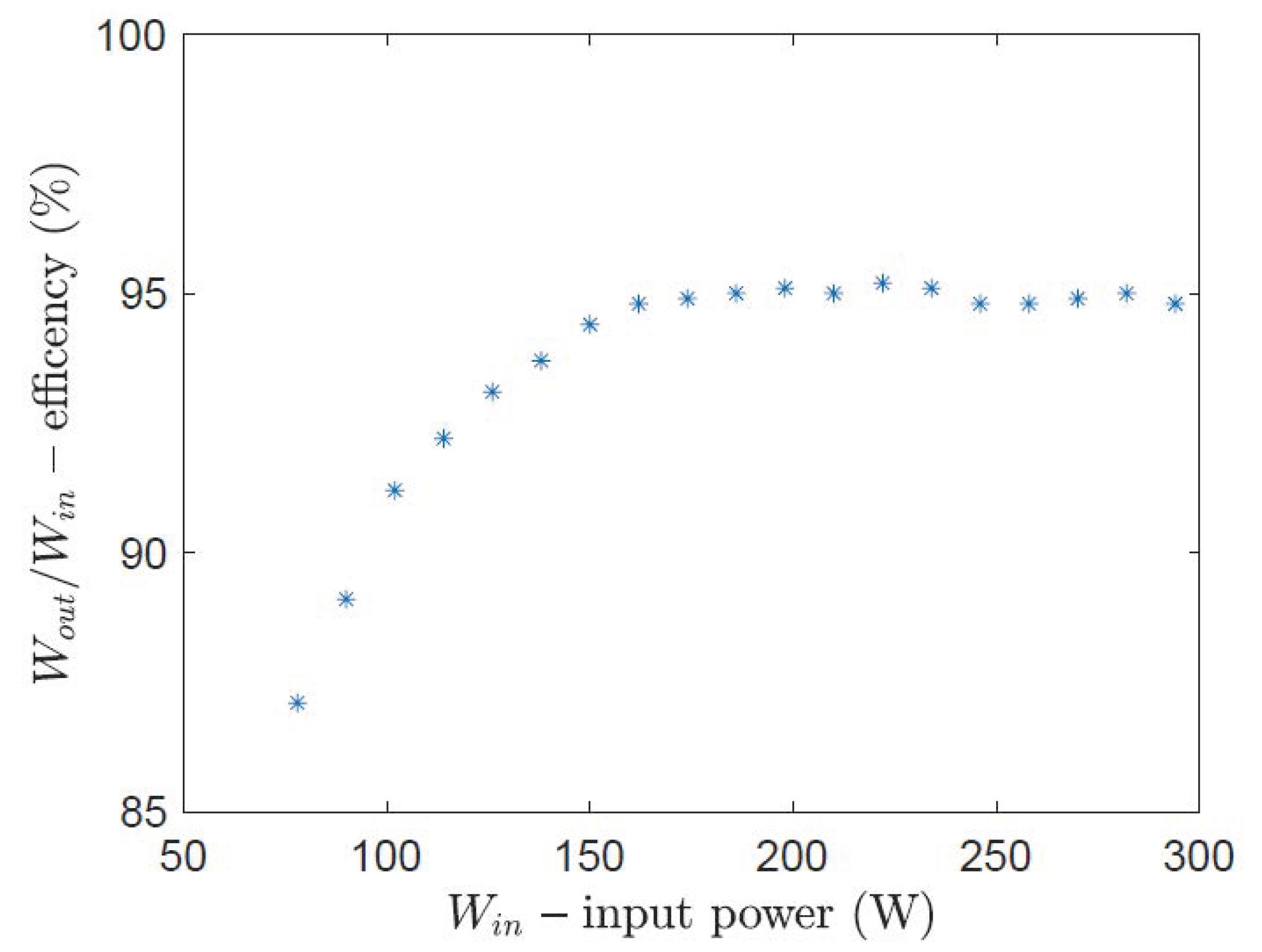
Figure 9 depicts the measured system efficiency for different values of input power. A good efficiency can be observed, about 95%, under nominal operating conditions.
In order to verify the effect of the outer loop, with integral action, the same start-up test was repeated using the control scheme of
Figure 3 with outer loop, and the results are given in
Figure 10 and
Figure 11. By comparing
Figure 6 with
Figure 10 and
Figure 7 with
Figure 11, it is evident that the external loop does not affect the system performance in terms of settling time and dynamic precision. Indeed, when we are working under nominal conditions, the external loop is as if it is disabled and the dynamics is imposed by the internal sliding mode loop. The external loop intervenes only when an unknown variation of load, input voltage or parameters takes place. In this last case, i.e., if unknown load and/or supply voltage variations or any other parameter variation occurs, an undesirable steady-state error takes place. For this reason, the outer loop, where the integral action is added in order to deal with this drawback, gives robustness to the proposed strategy. By means of this control scheme, load and supply voltage variation tests were carried out.
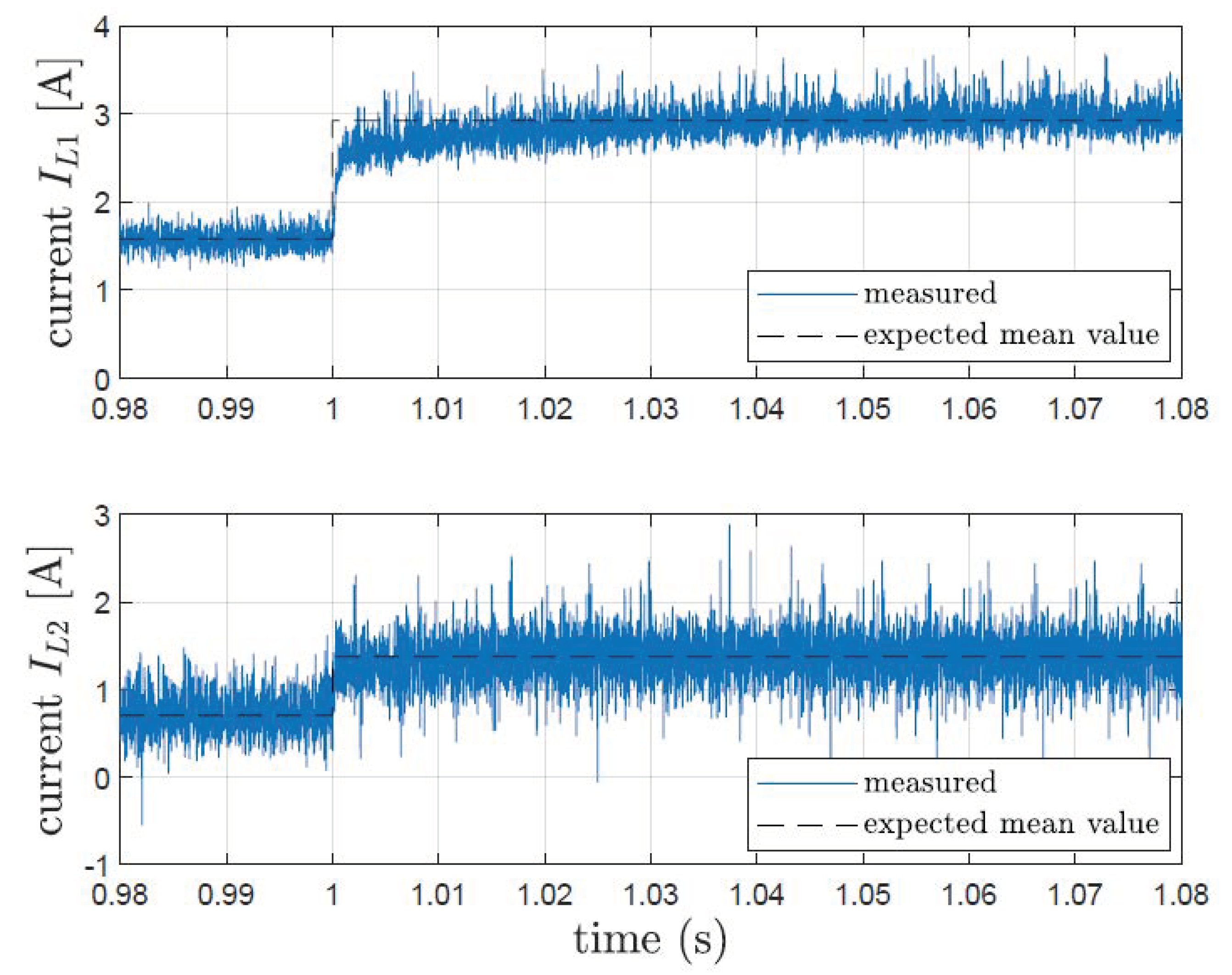
In particular, with regard to the load variations,
Figure 12 shows the voltages
and
and
Figure 13 shows the waveforms of the inductor currents
and
during a load variation from
to
. From these figures, the fast response of the system is evident. Moreover, due to the presence of the integral action, the steady-state error is totally compensated for. The only drawback coming from the use of the integral action is an increment of the settling time which is about 20 ms in this test, results higher than the one in the start-up test (2 ms). This is because the inner loop is faster than the outer loop.
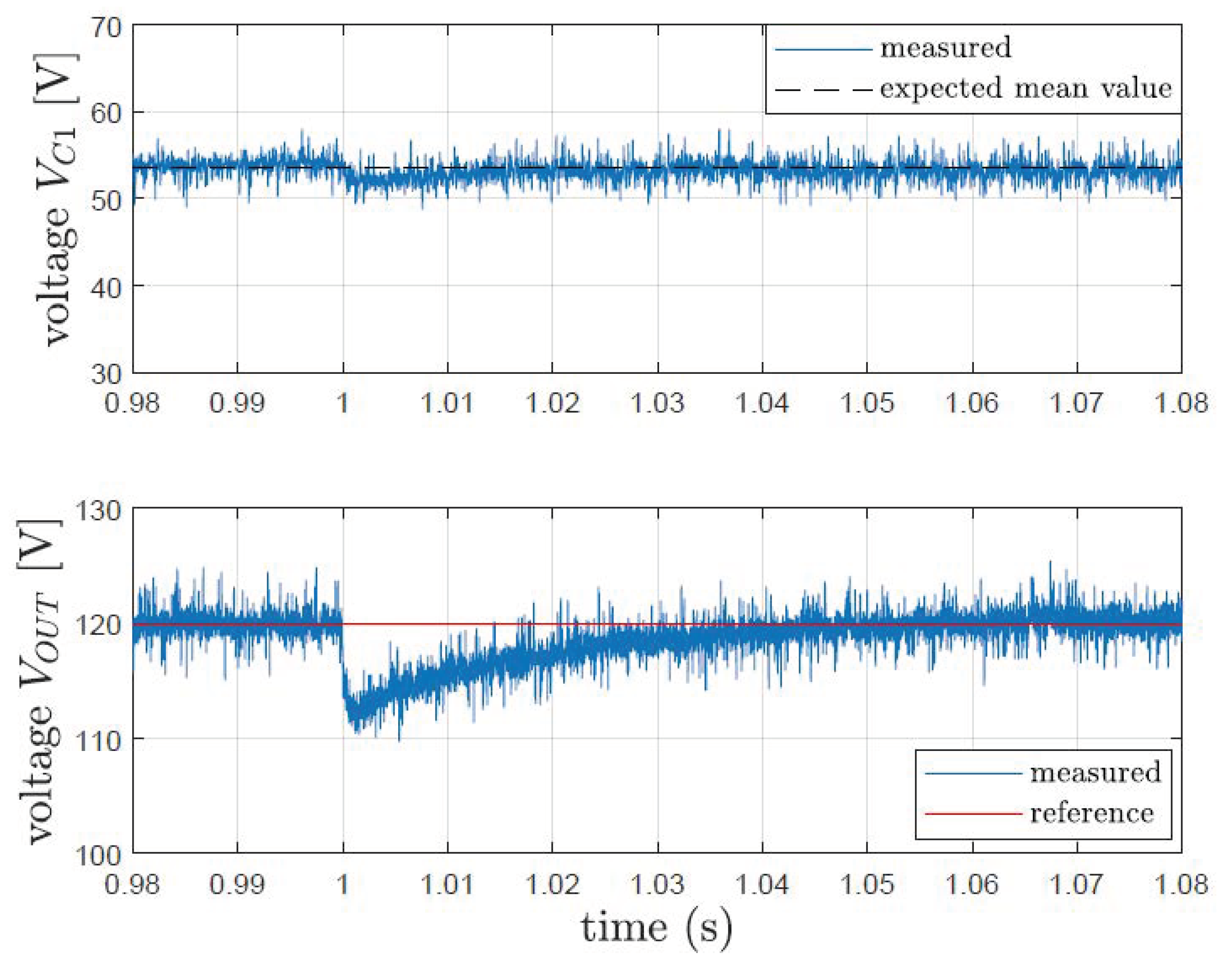
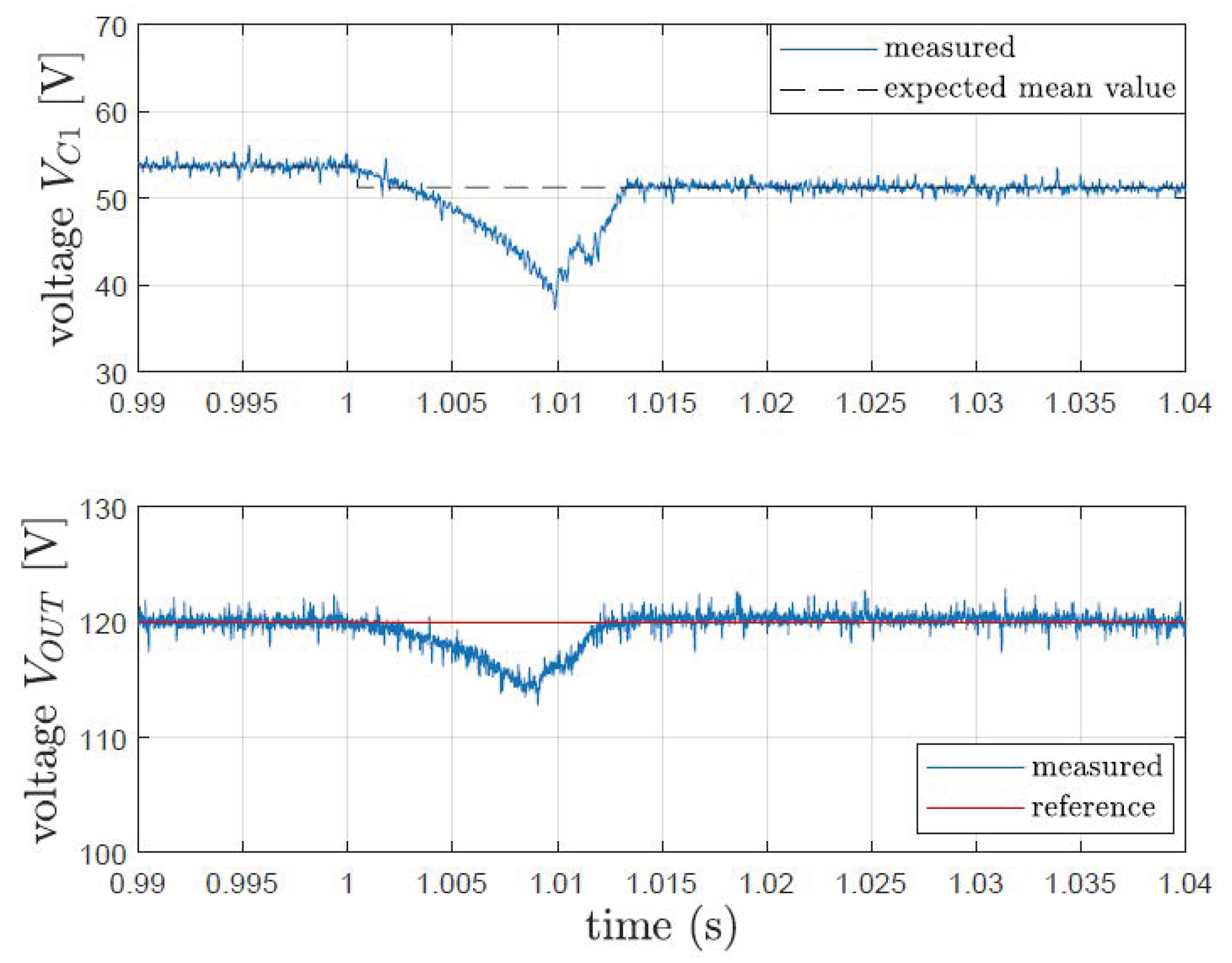
With regards to the supply voltage variations,
Figure 14 shows voltages
and
and
Figure 15 shows the waveforms of the inductor currents
and
during a supply voltage variation from
V to
V. Even in this case, the experimental results show that the system is able to deal with sudden (and unknown) supply voltage variations simulating, for example, a battery pack cell fault or shadow operating condition on a solar panel. In this test the resulting settling time is about 15 ms with an undershoot on the output voltage less than
, which is negligible.
All these results are summarized in
Table 2, where the main performance indexes (settling time and overshoot) are shown for all tests.
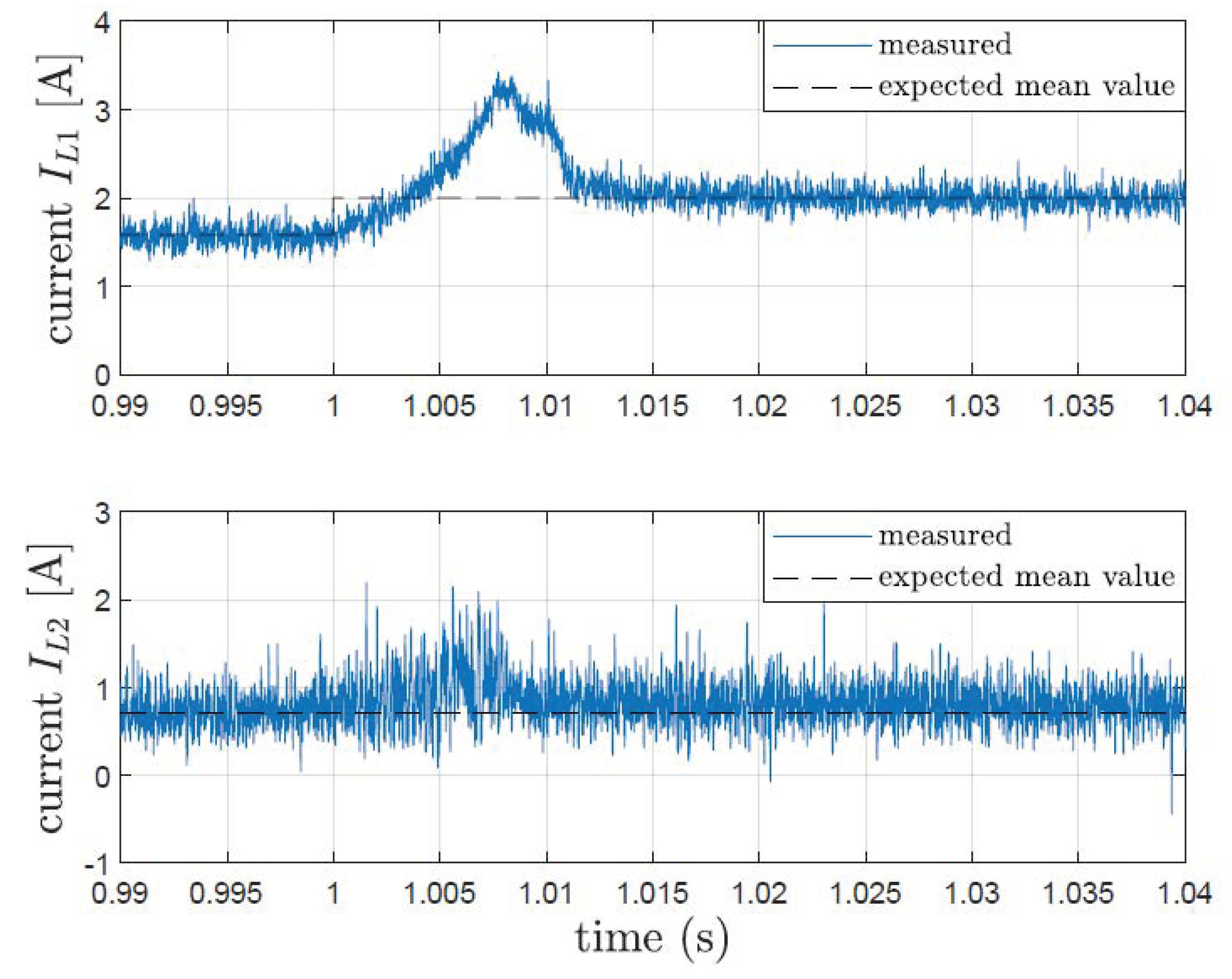
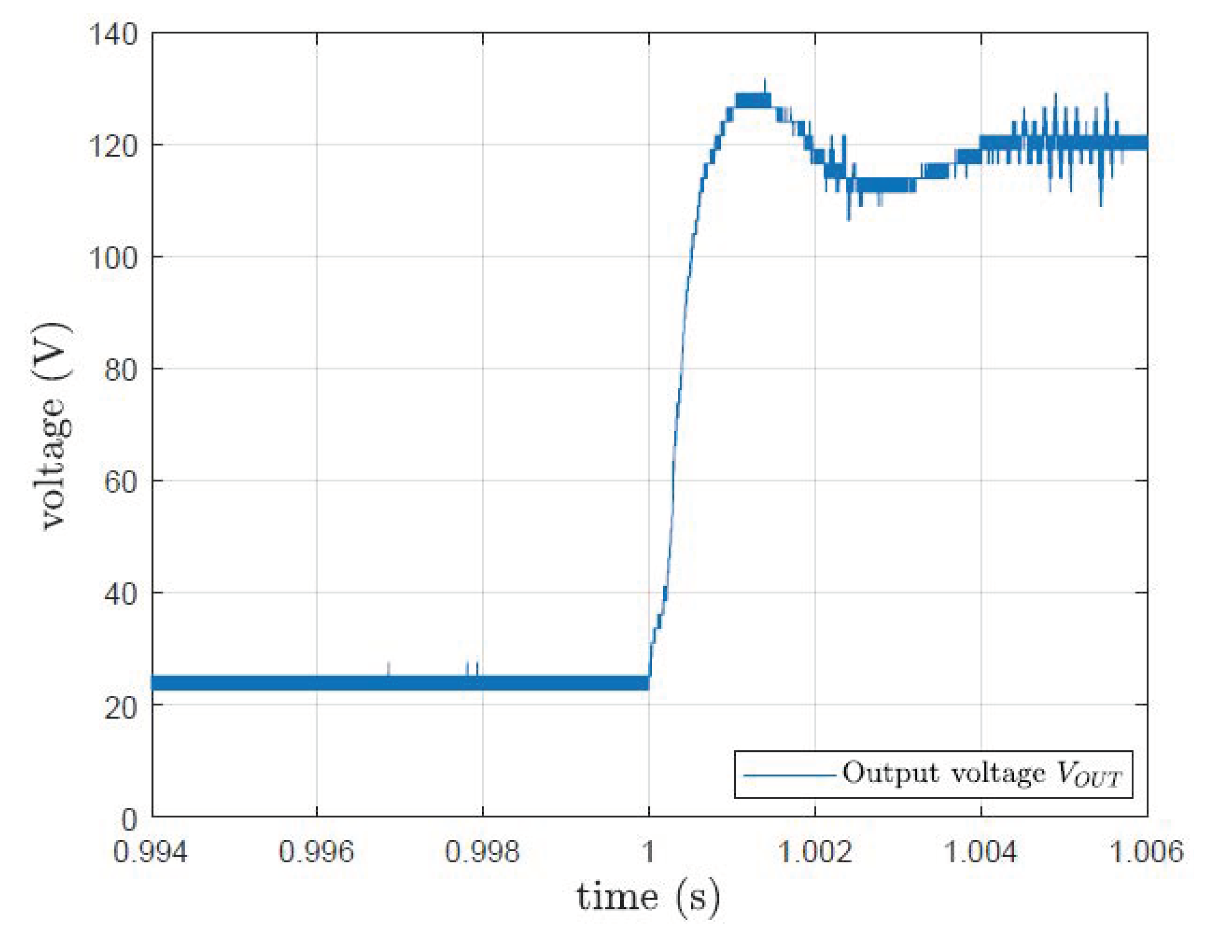
Finally, in order to compare the proposed technique with a conventional control strategy, a standard PID controller with constant PWM was implemented, and the same start-up test was carried out. In particular, the PID controller was tuned in order to obtain almost the same settling time obtained with the proposed strategy.
Figure 16 shows the output voltage
, while
Figure 17 shows the
and
currents during the same test. From these figures, the differences with the previous control strategy are evident. Indeed, the currents present a high overshoot that is not present in the currents of
Figure 7 and
Figure 11. Moreover, the output voltage presents a worst transience with respect to the one of
Figure 6 and
Figure 10, because from the comparison, a voltage overshoot is evident in
Figure 16 that is not present in
Figure 6 and
Figure 10, and even the settling time results are higher. All these results are summarized in
Table 2, where the numerical values of the overshoot and of the settling time are shown.
All these results show the capability of the system to cope with sudden changes in the nominal operating conditions. Indeed, the control system automatically stabilizes, by means of a new sliding regime, the system trajectories of the new equilibrium point. This confirm the effectiveness of the proposed control strategy.


 ,
, 


