Article

ZnO Nanorods as Antireflection Layers in Metal-Insulator-Semiconductor Solar Cells

by
Chung-Cheng Chang
1 and
Chia-Hong Huang
2,*
1
Department of Electrical Engineering, National Taiwan Ocean University, Keelung 202301, Taiwan
2
Department of Electronic Engineering, National Kaohsiung Normal University, Kaohsiung 824004, Taiwan
*
Author to whom correspondence should be addressed.
Electronics 2022, 11(13), 2068; https://doi.org/10.3390/electronics11132068
Submission received: 30 May 2022 / Revised: 24 June 2022 / Accepted: 28 June 2022 / Published: 1 July 2022

Abstract

:
One of the most promising techniques for manufacturing low-cost solar cells is a solution processing method. In this study, it is proposed that solution-grown ZnO nanorods (NRs) are used as antireflection coatings on metal-insulator-semiconductor (MIS) solar cells with sol-gel SiO2. Except Al electrodes prepared by thermal evaporation, no other vacuum process was utilized during fabrication. The ZnO NRs were produced with a hydrothermal method and suppressed Fresnel reflection. With the solution-grown ZnO NRs, it was observed the average reflectance of the MIS solar cell decreased from 38.7% to 15.8%, and the short circuit density (JSC) increased from 5.22 mA/cm2 to 6.71 mA/cm2 (28.4% enhancement). Meanwhile, the open circuit voltage (VOC) was improved from 0.39 V to 0.47 V owing to a passivation effect. The MIS solar cell with the ZnO NRs exhibited a 35.5% efficiency enhancement compared to that without ZnO NRs. The performance improvement in MIS solar cells with ZnO NRs could be due to multiple reflections of an incident light between the vertically arranged NRs, and then light coupling into the cell. The results show a potential application of ZnO NRs for the performance enhancement of MIS solar cells.

1. Introduction

Considerable light reflection exists at interface because of a refractive index mismatch between two substances. Such reflection leads to light loss so that optoelectronic devices, for instance solar cells, light-emitting devices and photodetectors, have an impact in performance. Hence, antireflective (AR) technologies are important aspects to eliminate reflection and improve performance in optical and optoelectronic applications. In general, antireflective coatings (ARCs) are composed of single-layer, multilayer or micro/nano structures. Single-layer ARCs are easy to produce but cannot decrease reflection in a broadband solar spectrum. In contrast, multilayer ARCs are complicated to prepare owing to the requirement of the refractive index and the precision of layer thickness. In addition, micro/nanostructured ARCs are fabricated by various techniques which are: imprinting [1], photolithography [2], molding [3], etching [4] or vacuum processing [5]. Unfortunately, these techniques are rather complex or not cheap for large areas and mass production.
On the other hand, zinc oxide (ZnO) is an attractive optoelectronic substance owing to its wide band-gap energy (3.3 eV), appropriate refractive index (n ≈ 2), large exciton-binding energy (60 meV), larger absorption coefficient, anisotropic growth and down-shifting effect. Especially, ZnO nanostructures, such as nanoparticles, nanorods (NRs), nanowires, nanowhisker and nanowalls, have attracted considerable research interest for optoelectronic applications [6,7,8,9,10,11,12,13,14,15,16]. Many methods have been used for the formation of ZnO NRs, such as pulsed laser deposition [17], chemical vapor deposition (CVD) [15,18], molecular beam epitaxy (MBE) [19] and aqueous solution methods [20,21]. Among these techniques, a hydrothermal method is a facile, fast, low-temperature, large-scale, substrate-independent and low-cost technique which can produce ZnO NRs on many kind of substrates via a ZnO seed layer. Furthermore, the surface is not textured during hydrothermal processing and thus is not damaged. Accordingly, ZnO NRs have been used in many kinds of solar cells, for example crystalline-Si, polycrystalline-Si, Cu(In,Ga)Se2, and organic solar cells, of which the short circuit density (JSC) is enhanced by 3.64 to 20% [22,23,24,25,26]. Though such, there are few reports on metal-insulator-semiconductor (MIS) solar cells with ZnO NR ARCs. In addition, a diffusion process used to produce a p-n junction structure in Si-based solar cells is a high-temperature and long-term technology, whereas MIS structure solar cell manufactured by low-temperature and short-term fabrication processes possess an inherent cost benefit compared with p-n junction solar cells. Therefore, accomplishing a study of the relationship between optical properties of ZnO NRs and the performance of the MIS solar cells is necessary and helpful for a comprehensive understanding of the relationship between ZnO nanorods and all kind of Si-based solar cells. In our previous report, MIS solar cells with the sol-gel derived SiO2 were successfully fabricated [27]. In this study, it is proposed that solution-grown ZnO NRs are used as ARCs on MIS solar cells with sol-gel spin-coated SiO2 layers. Except Al electrodes produced by thermal evaporation, MIS solar cells with ZnO NRs ARCs were manufactured by all-solution processing and thus exhibit a low-cost advantage in this study. The reflectance spectra implied that the ZnO NRs structure can efficiently minimize light reflection in a wide range of wavelengths from 300 nm to 1200 nm. Additionally, down-shifting processes in ZnO NRs permits the conversion of high-energy (UV) photons into many lower-energy (Green–Red) ones so that the additional electron-hole pairs are generated in the active layer and thus increase in the efficiency of the solar cell. Under these circumstances, it was reported that ZnO NRs structures exhibit both broadband, omnidirectional AR and down-shifting properties so that solar cells with ZnO NRs exhibit excellently photovoltaic performance [15,28]. As a result, the short circuit density (JSC) and power conversion efficiency (PCE) were increased to 6.71 mA/cm2 (28.4% enhancement) and 1.26% (35.5% enhancement), respectively, which were due to the enhanced light absorption. Meanwhile, the open circuit voltage (VOC) was raised from 0.39 V to 0.47 V, which could be attributed to a passivation effect of ZnO NRs [29]. These results indicate the ZnO NRs structure could be a promising candidate to enhance the performance of the MIS solar cell.

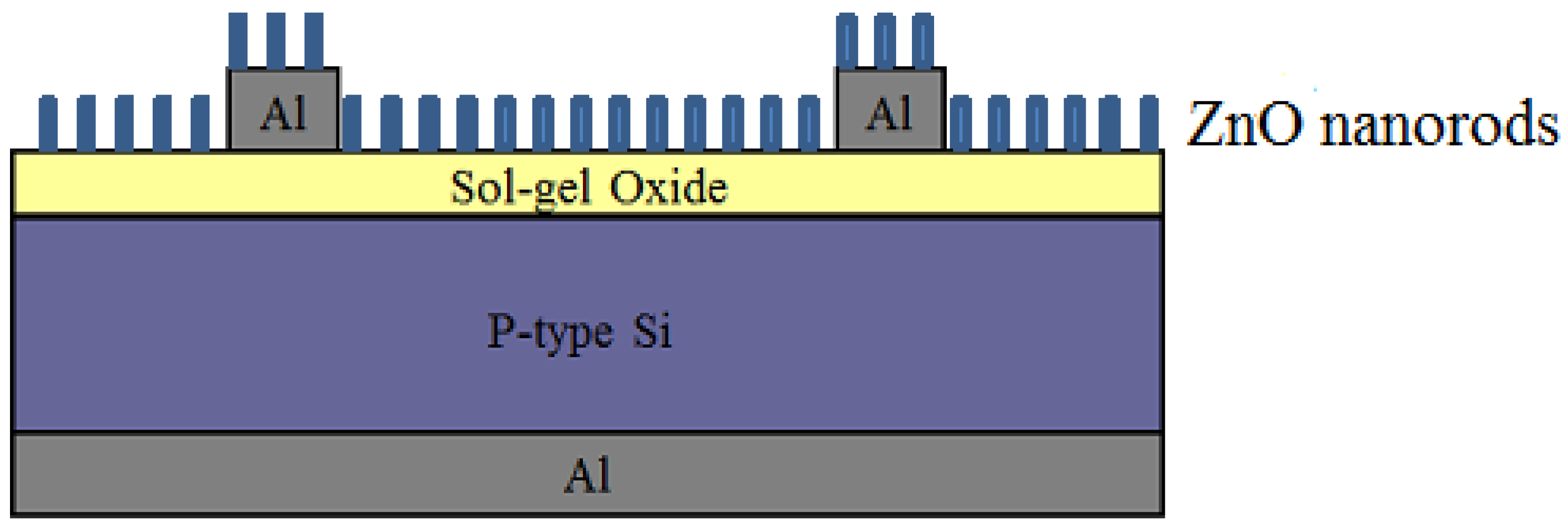
2. Materials and Methods

A MIS solar cell was produced on a (100) p-type Si substrate according to the method reported in literature [27]. A sol-gel solution was prepared by the acid catalyzed hydrolysis of tetraethylorthosilicate (TEOS) in alcohol solution. The solution was diluted by de-ionized (DI) water and then aged. Wet SiO2 thin films were spin-coated on Si substrates, and then dried at 60 °C. Sol-gel SiO2 layers were heated at 450 °C for 1 h. After these treatments, aluminum (Al) front electrode was deposited by thermal evaporation. Al was also used as the back contact.
A ZnO seed layer was grown on the surface of the MIS solar cell by a sol-gel method. Firstly, equivalent molar zinc acetate dehydrate (Zn(C2H3O2)2·2H2O) and monoethanolamine (MEA) were dissolved in ethylalcohol, and then stirred for 2 h at room temperature. Subsequently, a wet ZnO seed layer was spin-coated on the surface of the MIS solar cell for 20 s with 1000 rpm. Then the cell was dried at 90 °C for 10 min. Finally, the gel-coated cell was annealed at 300 °C for 1 h. A ZnO seed layer was obtained on the surface of the MIS solar cell.
ZnO NRs were hydrothermally synthesized on as-manufactured cells. A hydrothermal solution made up of equivalent molar zinc nitrate hexahydrate (Zn(NO3)2·6H2O) and hexamethylene tetramine (C6H12N4) in 100 mL of DI water was stirred for 20 min. The concentration of the aqueous solution was determined to be 10, 20, 30 and 40 mM. Each solution was stirred for 2 h, and then kept at room temperature for one day. Four samples were immersed into the different solutions (10, 20, 30 and 40 mM) at 95 °C for 30 min. Moreover, another four samples were immersed into the solution with the concentration of 30 mM at 95 °C for 15, 30, 60 and 120 min, respectively. After these treatments, all samples were rinsed with DI water and dried at room temperature. The schematic cross-sectional diagram of the MIS solar cell with ZnO NRs is shown in Figure 1. Furthermore, it is emphasized that MIS solar cells are without back surface fields in this study.
The crystalline structure of the ZnO NRs was examined by X-ray diffraction (XRD) (X’Pert Pro MPD, Panalytical, Almelo, The Netherlands) with CuKα radiation (40 kV and 30 mA) for 2θ values of over 20° to 80°. The surface and cross-sectional microstructures of the ZnO NRs were characterized by field-emission scanning electron microscope (FESEM) (S-4800, Hitachi, Tokyo, Japan) operating at 15 kV. The surface reflectance spectra were conducted by using an UV/VIS/NIR spectrophotometer (UV-3150, Shimadzu, Tokyo, Japan). The morphology of the ZnO NRs was analyzed by atomic force microscope (AFM) (Dimension ICON, Bruker, Tucson, AZ, USA). The current-voltage curves of MIS solar cells were measured by Keitheley 4200 semiconductor analyzer under AM 1.5G illumination with the power density of 100 mW/cm2 at 25 °C.

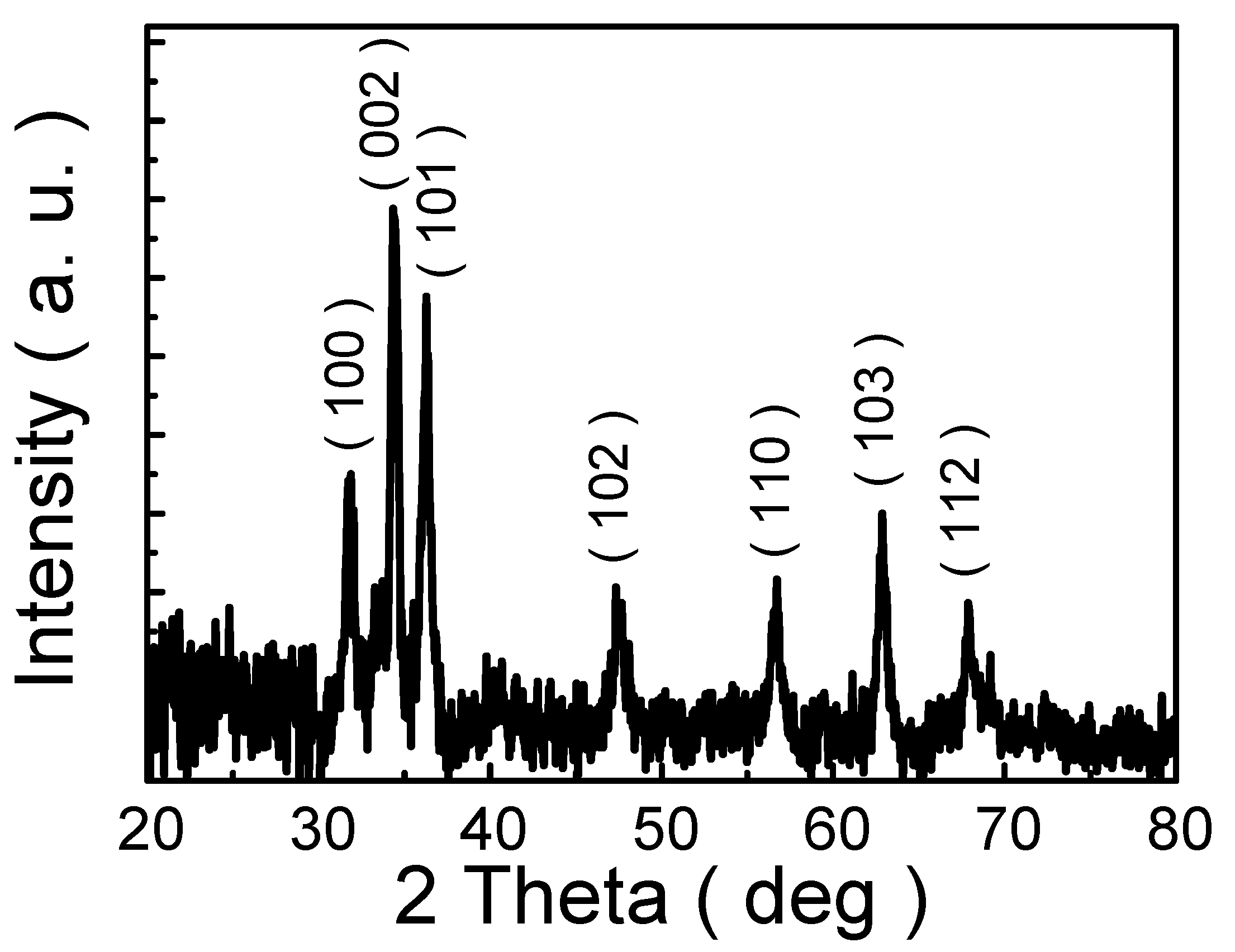
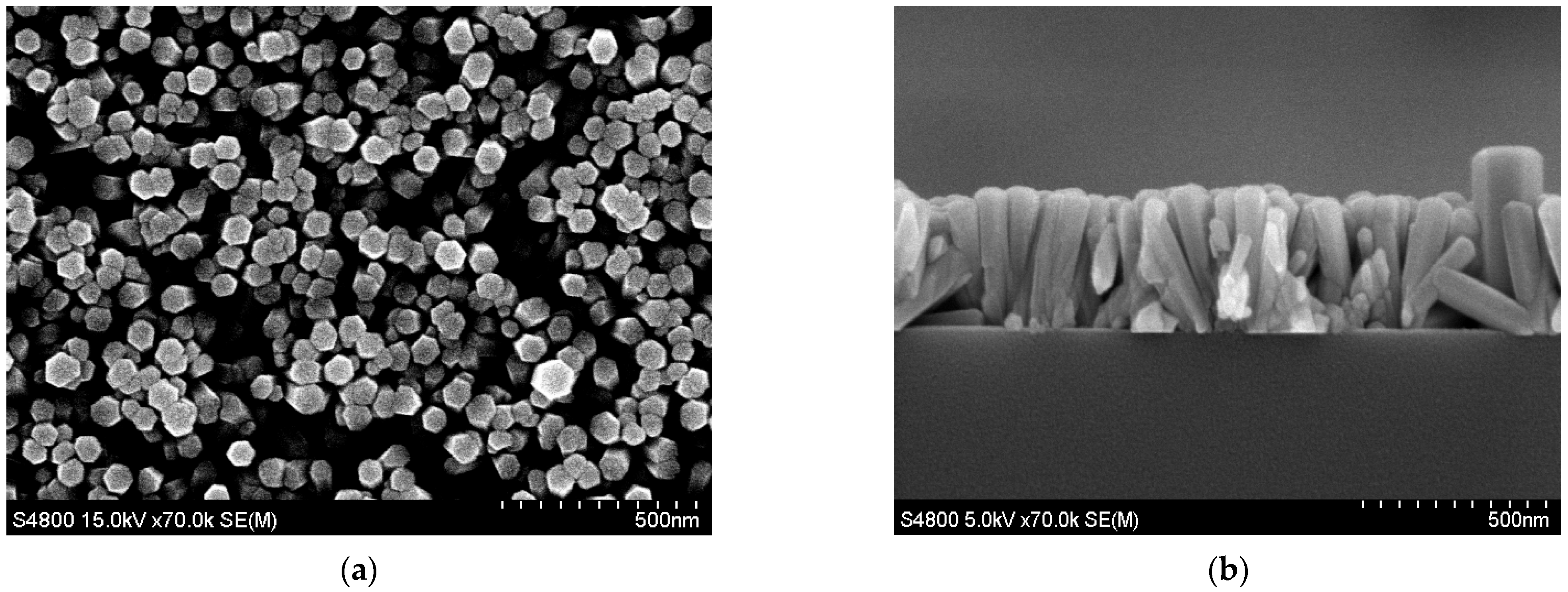
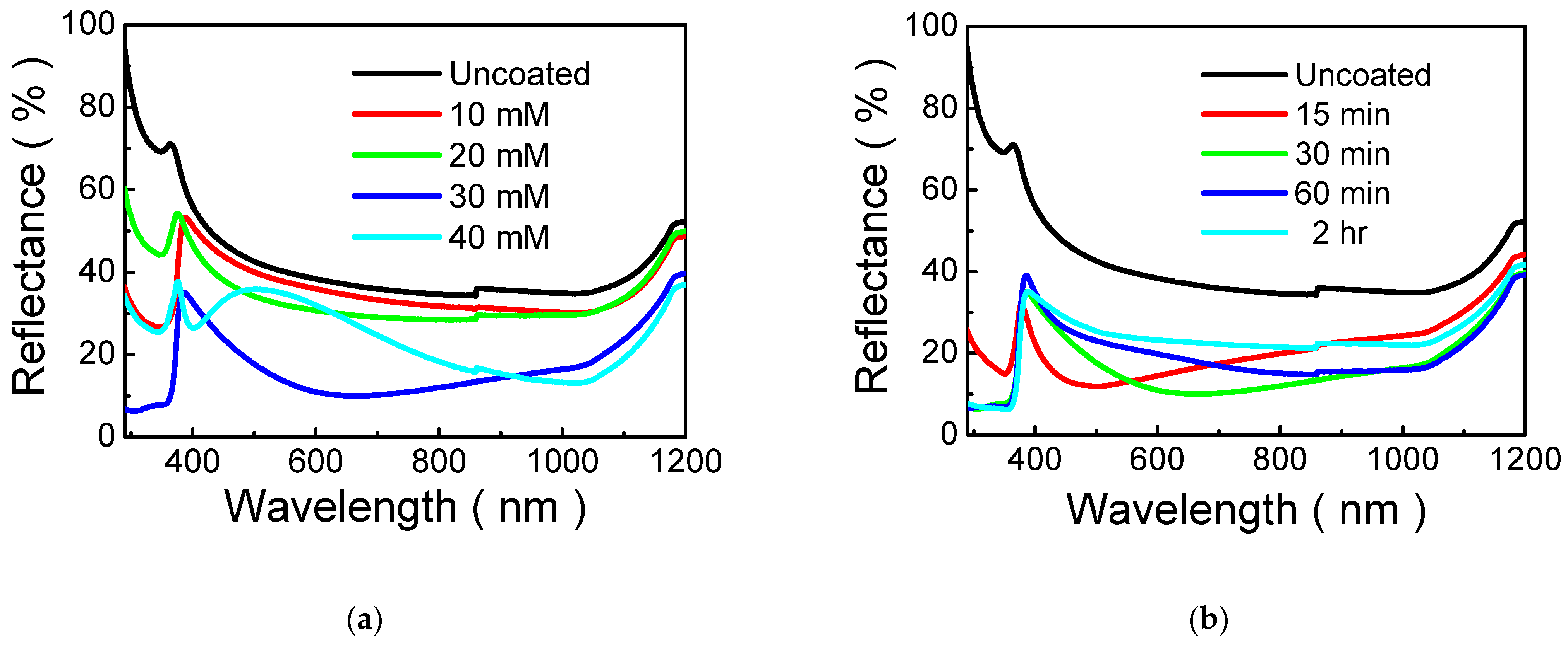
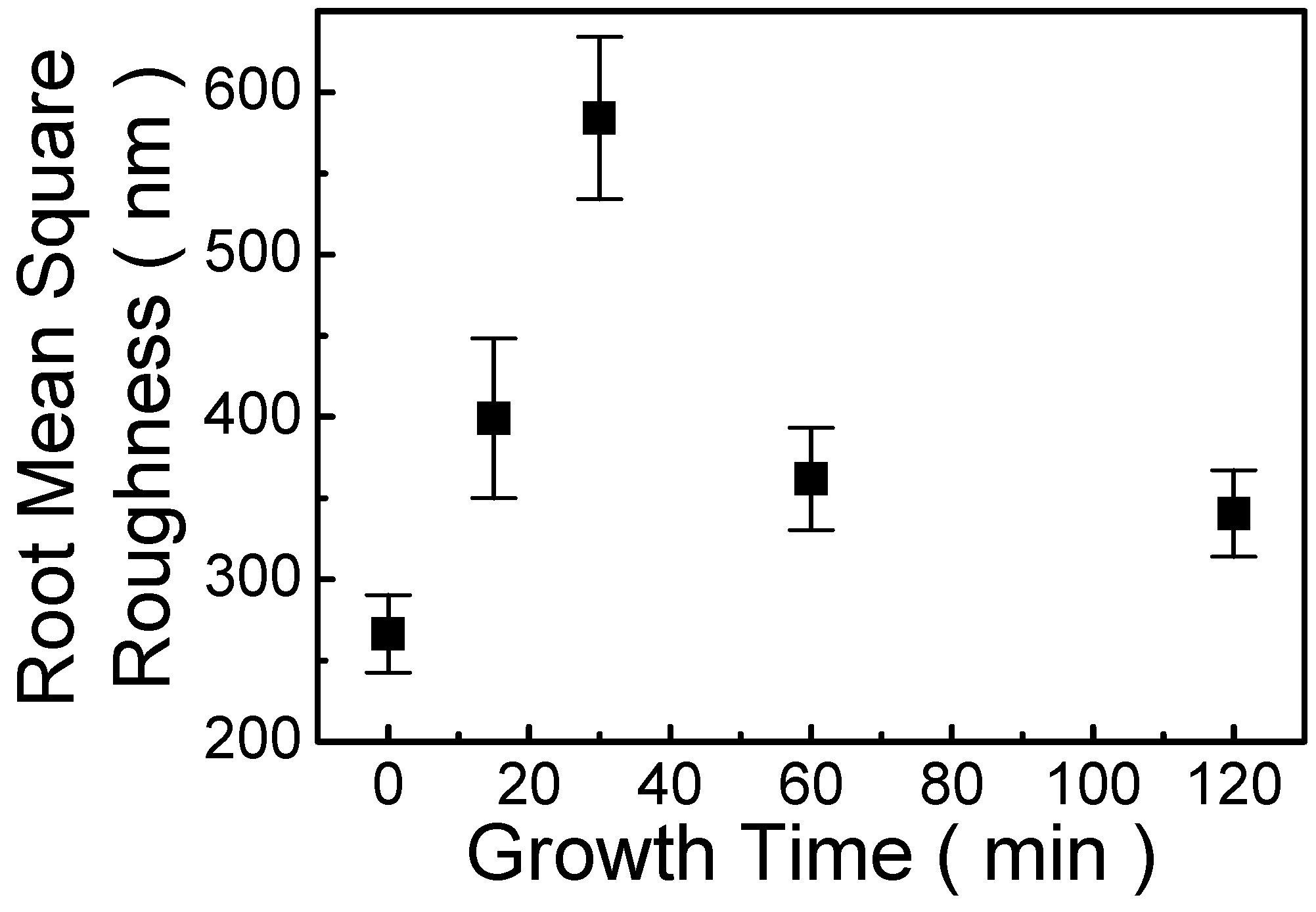
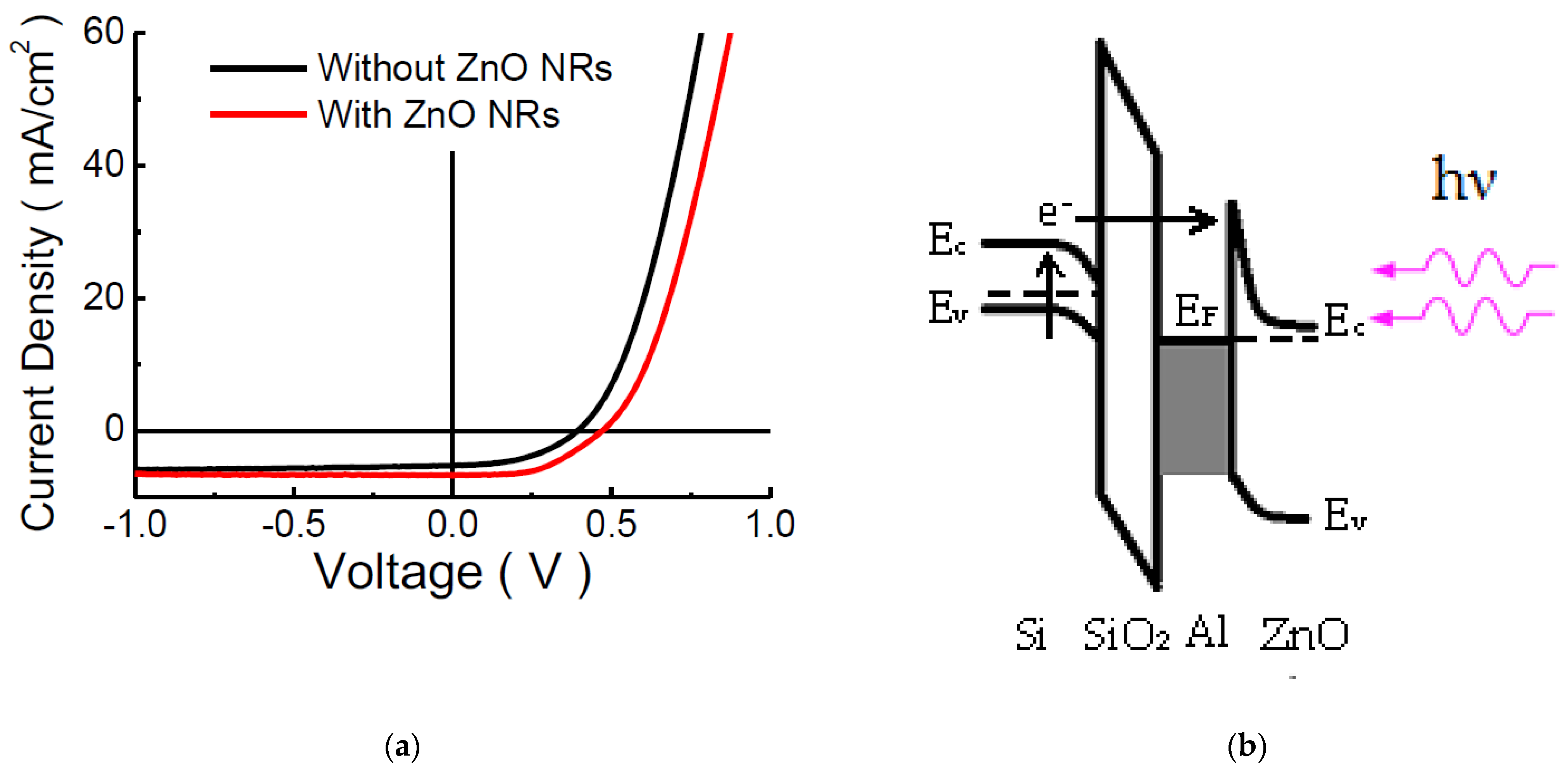
3. Results and Discussion

Figure 2 shows an XRD pattern of ZnO nanorods (NRs). XRD spectra of the ZnO NRs exhibit three pronounced peaks at 31.7°, 34.4°, and 36.2°, which corresponds to ZnO (100), (002), and (101) planes, respectively. Particularly, XRD spectra illustrates a stronger (002) peak, which reveals that ZnO NRs possess a high orientation with the c-axis perpendicular to the surface. Moreover, relatively small peaks observed at 47.5°, 56.5°, 62.8°, and 67.8° are associated with the reflections from the (102), (110), (103), and (112) planes of ZnO NRs, respectively. Based on the XRD result, the crystallographic phase of ZnO nanorods belongs to the polycrystalline wurtzite structure [30], confirming the production of high-quality ZnO NRs.
Figure 3a reveals the top-view SEM image of ZnO NRs, in which ZnO NRs are distributed with high density. Furthermore, all ZnO NRs are terminated with a hexagonal flat top. The average diameter was about 80 nm. Moreover, Figure 3b illustrates the cross-sectional SEM image of ZnO NRs. ZnO NRs with comparatively high density were observed on the substrate and the average length was around 395 nm. As shown in Figure 3b, the ZnO NRs are vertical to thesurface, which is ascribed to the underneath seed layer. Consequently, the result in Figure 3b is consistent with that in Figure 2.
Figure 4a demonstrates the reflectance spectra of ZnO NRs produced in the different solutions (10 mM, 20 mM, 30 mM and 40 mM). For the uncoated cell, all reflectance values were above 30% from 250 nm to 1200 nm wavelengths. As shown in Figure 4a, the reflectance was decreased over the wide wavelength range by growing ZnO NRs on the surface. The average reflectances of the ZnO NRs prepared in different solutions (uncoated, 10 mM, 20 mM, 30 mM and 40 mM) were calculated to be 38.66%, 35.11%, 31.79%, 15.84% and 23.33%, respectively. The average reflectance initially decreased with the increase in the solution concentration. However, for ZnO NRs grown in 40 mM solution, the average reflectance increased, which indicated that there was an optimal solution concentration for optimum decreasing in light reflection. In addition, the cell coated by using 30 mM solution reached the lowest reflectance value at 660 nm, about 10%, which was 3.4 times lower than that on the uncoated cell, and exhibited superior AR characteristics in the visible region. Such low reflectance was due to the textured surface. Besides, the reflectance below 390 nm wavelength was obviously dropped because of the intrinsic absorption of ZnO NRs.
Figure 4b depicts the reflectance spectra of ZnO NRs for the different growth times. The average reflectances of ZnO NRs for the growth times of 0 (uncoated), 15, 30, 60 and 120 min were evaluated to be 38.66%, 19.35%, 15.84%, 19.32% and 23.94%, respectively. In Figure 4b, the uncoated cell displayed a high average reflectance, 38.66%, as mentioned above, whereas after coating the surface for the growth time of 15 min, the average reflectance was reduced to 19.35%, which was ascribed to the textured surface. As seen in Figure 4b, a significant reduction in the average reflectance to 15.84% was achieved for ZnO NRs grown for 30 min. Nevertheless, the average reflectance of ZnO NRs contrariwise increased as the growth time is more than 30 min. These results also indicate that an optimal growth time for ZnO NRs is required for an effective reduction in light reflection for MIS solar cells.
Figure 5 presents root mean square (RMS) values of ZnO NRs grown for the various growth times (15, 30, 60 and 120 min) from AFM measurements. AFM images in Figure S1 shows that the roughness of ZnO NRs changes significantly as the growth time is varied. RMS roughness was measured on an area of 30 × 30 μm2. From AFM measurements, we also found that RMS roughness values were 266, 399, 584, 362 and 341 nm for ZnO NRs for the different growth times (uncoated, 15, 30, 60 and 120 min), respectively, as shown in Figure 5. RMS roughness value initially increased with the growth time. However, as the growth time was more than 30 min, RMS roughness gradually decreased. The length of the ZnO NRs is generally influenced by growth time, solution concentration and growth temperature. Furthermore, RMS roughness values of the ZnO layer rise with increasing the solution concentration [31]. It is, therefore, proposed that the length of ZnO NR initially increases with the growth time under almost constant concentration conditions so that the surface becomes rougher. Nevertheless, after the optimal growth time (30 min), the growth rate of ZnO NRs lowers because of the reduction in the amount of reactants (under lower concentration condition). Accordingly, the deviation from the mean length of ZnO NRs becomes smaller, and hence the surface roughness lowers. The result in Figure 5 is in good agreement with that in Figure 4b.
Figure 6a,b indicate the current density-voltage (J-V) curves of MIS solar cells with and without ZnO NRs ARC under AM1.5G conditions and the energy band diagram of MIS solar cells with ZnO NRs ARCs, respectively. The short circuit current density (JSC) was raised from 5.22 to 6.71 mA/cm2 (28% enhancement) and the power conversion efficiency (PCE) was enhanced from 0.93 to 1.26% (35% enhancement), which were attributed to the enhancement of light absorption. Theoretically, if the spacing between nanostructures is less than light wavelength, then the textured surface of nanostructures can be regarded as layers with a gradually changing refractive index so that the optical properties can be estimated by effective medium approximation [32]. In other words, light experiences multiple reflections between neighboring ZnO NRs, and thus is trapped and coupled into the surface of the MIS solar cell. Therefore, the ZnO NRs arrays act as a light trap and increase light absorption and hence improve JSC and PCE. On the other hand, the open circuit voltage (VOC) was increased from 0.39 to 0.47 V. The increment in VOC could be due to the passivation effect of ZnO NRs [24]. Passivation decreases the recombination current and increases the shunt resistance (Rsh) and thus improves the VOC of the MIS solar cell. Correspondingly, the fill factor (FF) was improved from 0.45 to 0.5. Table 1 shows photovoltaic parameters of MIS solar cells with ZnO NRs and without ZnO NRs. In general, fill factor (FF) is dependent on the series resistance (Rs) and the shunt resistance (Rsh). In this study, Rs was larger and almost fixed after coating ZnO NRs. Moreover, Rs includes ohmic loss in the front contacts, insulator-semiconductor interface, and bulk equivalent resistance of the solar cell. Therefore, it is suggested that the more elaborate front contact electrode patterns and the lower interface state density are required to improve Voc and FF in future. The PCE value for a MIS solar cell is not high in this study, which could result from a higher interface state density because of the low growth temperature (450 °C), but the results exhibit the effective use of hydrothermally synthesized ZnO NRs as ARCs and sol-gel derived SiO2 as insulators (all solution-processed techniques) in MIS solar cells. In addition, it is expected that the morphology of the ZnO NRs could be altered by the concentration of the aqueous solution and the growth time. With the decrease in the solution concentration and the increase in the growth time, the top morphology of the ZnO NRs could be changed from hexagonal flat to another type of nanostructure so that the performance of the MIS solar cell is further improved in future.

4. Conclusions

We manufactured ZnO NRs used as ARCs by hydrothermal method on MIS solar cells with sol-gel spin-coated SiO2. Except Al electrodes deposited by thermal evaporation, no other vacuum process was applied during fabrication. The MIS solar cells with ZnO NRs exhibited superior AR performance. The JSC and PCE were increased to 6.7 mA/cm2 (28% enhancement) and 1.26% (35% enhancement), respectively, which were attributed to the enhanced light absorption. Meanwhile, VOC was improved from 0.39 to 0.46 V, which was probably ascribed to the passivation effect. Besides, FF was enhanced from 45 to 50%. The results indicate that the MIS solar cell with sol-gel spin-coated SiO2 and solution-grown ZnO NRs have considerable potential for low-cost photovoltaic applications, and provide a comprehensive understanding of the relationship between ZnO NRs and MIS Si solar cells. Furthermore, it is believed that through optimizations of synthesis parameters, it could further decrease reflectance and improve photovoltaic performance for highly efficient MIS solar cells in the future.

Supplementary Materials

The following supporting information can be downloaded at: https://www.mdpi.com/article/10.3390/electronics11132068/s1. Figure S1: The AFM images of ZnO nanorods for the different growth times: (a) 0 min (uncoated); (b) 15 min; (c) 30 min; (d) 60 min; (e) 120 min. (Bruker, Dimension ICON, Tucson, AZ, USA).

Author Contributions

Conceptualization, C.-C.C. and C.-H.H.; methodology, C.-H.H.; validation, C.-C.C. and C.-H.H.; formal analysis, C.-C.C. and C.-H.H.; investigation, C.-H.H.; resources, C.-C.C.; writing—original draft preparation, C.-H.H.; writing—review and editing, C.-C.C. and C.-H.H.; supervision, C.-C.C.; project administration, C.-C.C.; funding acquisition, C.-C.C. All authors have read and agreed to the published version of the manuscript.

Funding

This research received no external funding.

Acknowledgments

The authors wish to thank Jung-Hui Tsai for helpful discussions in photovoltaic analysis.

Conflicts of Interest

The authors declare no conflict of interest.

References

  1. Leem, J.W.; Kim, S.; Lee, S.H.; Rogers, J.A.; Kim, E.; Yu, J.S. Efficiency enhancement of organic solar cells using hydrophobic antireflective inverted moth-eye nanopatterned PDMS films. Adv. Energy Mater. 2014, 4, 1301315. [Google Scholar] [CrossRef]
  2. Kwon, Y.W.; Park, J.; Kim, T.; Kang, S.H.; Kim, H.; Shin, J.; Jeon, S.; Hong, S.W. Flexible near-field nanopatterning with ultrathin, conformal phase masks on nonplanar substrates for biomimetic hierarchical photonic structures. ACS Nano 2016, 10, 4609–4617. [Google Scholar] [CrossRef] [PubMed]
  3. Dudem, B.; Heo, J.H.; Leem, J.W.; Yu, J.S.; Im, S.H. CH3NH3PbI3 planar perovskite solar cells with antireflection and self-cleaning function layers. J. Mater. Chem. A 2016, 4, 7573–7579. [Google Scholar] [CrossRef]
  4. Rahman, A.; Ashraf, A.; Xin, H.; Tong, X.; Sutter, P.; Eisaman, M.D.; Black, C.T. Sub-50-nm self-assembled nanotextures for enhanced broadband antireflection in silicon solar cells. Nat. Commun. 2015, 6, 5963. [Google Scholar] [CrossRef] [Green Version]
  5. Kanamori, Y.; Ishimori, M.; Hane, K. High efficient light-emitting diodes with antireflection subwavelength gratings. IEEE Photon. Technol. Lett. 2002, 14, 1064–1066. [Google Scholar] [CrossRef]
  6. Lee, Y.-J.; Ruby, D.S.; Peters, D.W.; McKenzie, B.B.; Hsu, J.W.P. ZnO nanostructures as efficient antireflection layers in solar cells. Nano Lett. 2008, 8, 1501–1505. [Google Scholar] [CrossRef]
  7. Lee, S.-W.; Jeong, M.-C.; Myoung, J.-M.; Chae, G.-S.; Chung, I.-J. Magnetic alignment of ZnO nanowires for optoelectronic device applications. Appl. Phys. Lett. 2007, 90, 133115. [Google Scholar] [CrossRef]
  8. So, H.; Senesky, D.G. ZnO nanorod arrays and direct wire bonding on GaN surfaces for rapid fabrication of antireflective, high-temperature ultraviolet sensors. Appl. Surf. Sci. 2016, 387, 280–284. [Google Scholar] [CrossRef]
  9. Park, W.I.; Yi, G.-C. Electroluminescence in n-ZnO Nanorod Arrays Vertically Grown on p-GaN. Adv. Mater. 2004, 16, 87–90. [Google Scholar] [CrossRef]
  10. Law, M.; Greene, L.E.; Johnson, J.C.; Saykally, R.; Yang, P. Nanowire dye-sensitized solar cells. Nat. Mater. 2005, 4, 455–459. [Google Scholar] [CrossRef]
  11. Khan, R.; Althubeiti, K.; Zulfiqar; Afzal, A.M.; Rahman, N.; Fashu, S.; Zhang, W.; Khan, A.; Zheng, R. Structure and magnetic properties of (Co, Ce) co-doped ZnO-based diluted magnetic semiconductor nanoparticles. J. Mater. Sci. Mater. Electron. 2021, 32, 24394–24400. [Google Scholar] [CrossRef]
  12. Afzal, A.M.; Javed, Y.; Hussain, S.; Ali, A.; Yaqoob, M.Z.; Mumtaz, S. Enhancement in photovoltaic properties of bismuth ferrite/zinc oxide heterostructure solar cell device with graphene/indium tin oxide hybrid electrodes. Ceram. Int. 2020, 46, 9161–9169. [Google Scholar] [CrossRef]
  13. Zubair, M.; Khan, A.; Hua, T.; Ilyas, N.; Fashu, S.; Afzal, A.M.; Safeen, M.A.; Khan, R. Oxygen vacancies induced room temperature ferromagnetism and enhanced dielectric properties in Co and Mn co-doped ZnO nanoparticles. J. Mater. Sci. Mater. Electron. 2021, 32, 9463–9474. [Google Scholar] [CrossRef]
  14. Yu, X.; Wang, D.; Lei, D.; Li, G.; Yang, D. Efficiency improvement of silicon solar cells enabled by ZnO nanowhisker array coating. Nanoscale Res. Lett. 2012, 7, 306. [Google Scholar] [CrossRef] [Green Version]
  15. Gholizadeh, A.; Reyhani, A.; Parvin, P.; Mortazavi, S.Z. Efficiency enhancement of ZnO nanostructure assisted Si solar cell based on fill factor enlargement and UV-blue spectral down-shifting. J. Phys. D Appl. Phys. 2017, 50, 185501. [Google Scholar] [CrossRef]
  16. Huang, M.H.; Mao, S.; Feick, H.; Yan, H.; Wu, Y.; Kind, H.; Weber, E.; Russo, R.; Yang, P. Room-temperature ultraviolet nanowire nanolasers. Science 2001, 292, 1897–1899. [Google Scholar] [CrossRef] [Green Version]
  17. Kawakami, M.; Hartanto, A.B.; Nakata, Y.; Okada, T. Synthesis of ZnO nanorods by nanoparticle assisted pulsed-laser deposition. Jpn. J. Appl. Phys. 2003, 42, L33–L35. [Google Scholar] [CrossRef]
  18. Park, W.I.; Yi, G.-C.; Kim, J.-W.; Park, S.-M. Schottky nanocontacts on ZnO nanorod arrays. Appl. Phys. Lett. 2003, 82, 4358–4360. [Google Scholar] [CrossRef] [Green Version]
  19. Kim, M.S.; Nam, G.; Leem, J.Y. Photoluminescence studies of ZnO nanorods grown by plasma-assisted molecular beam epitaxy. J. Nanosci. Nanotechnol. 2013, 13, 3582–3585. [Google Scholar] [CrossRef]
  20. Chung, R.-J.; Lin, Z.-C.; Lin, C.-A.; Lai, K.-Y. Study of an antireflection surface constructed of controlled ZnO nanostructures. Thin Solid Films 2014, 570, 504–509. [Google Scholar] [CrossRef]
  21. Lin, Z.-X.; Huang, B.; He, G.-N.; Yang, W.-F.; He, Q.-Y.; Li, L.-X. High efficiency enhancement of multi-crystalline silicon solar cells with syringe-shaped ZnO nanorod antireflection layers. Thin Solid Films 2018, 653, 151–157. [Google Scholar] [CrossRef]
  22. Hsueh, H.-T.; Chen, Y.-H.; Lin, Y.-D.; Lai, K.-C.; Chen, J.-W.; Wu, C.-L. Integration of flower-like ZnO nanostructures with crystalline-Si interdigitated back contact photovoltaic cell as a self-powered humidity sensor. Appl. Phys. Lett. 2013, 103, 213109. [Google Scholar] [CrossRef]
  23. Chen, J.Y.; Sun, K.W. Growth of vertically aligned ZnO nanorod arrays as antireflection layer on silicon solar cells. Sol. Energy Mater. Sol. Cells 2010, 94, 930–934. [Google Scholar] [CrossRef]
  24. Dong, W.J.; Huang, C.Y.; Wei, T.X.; Zhang, Y.; Zhang, K.N.; Sun, Y.; Chen, X.; Dai, N. Nondestructively decorating surface textured silicon with nanorod arrays for enhancing light harvesting. Phys. Status Solidi A 2013, 210, 2542–2549. [Google Scholar] [CrossRef]
  25. Jheng, B.-T.; Liu, P.-T.; Wu, M.-C. Efficiency enhancement of non-selenized Cu(In,Ga)Se2 solar cells employing scalable low-cost antireflective coating. Nanoscale Res. Lett. 2014, 9, 331. [Google Scholar] [CrossRef] [PubMed] [Green Version]
  26. Kim, S.; Koh, J.H.; Yang, X.; Chi, W.S.; Park, C.; Leem, J.W.; Kim, B.; Seo, S.; Kim, Y.; Yu, J.S.; et al. Enhanced Device Efficiency of Bilayered Inverted Organic Solar Cells Based on Photocurable P3HTs with a Light-Harvesting ZnO Nanorod Array. Adv. Energy Mater. 2014, 4, 1301338. [Google Scholar] [CrossRef]
  27. Huang, C.-H.; Chang, C.-C.; Tsai, J.-H. MOS Solar Cells with Oxides Deposited by Sol-Gel Spin-Coating Techniques. Semiconductors 2013, 47, 835–837. [Google Scholar] [CrossRef]
  28. Kim, S.H.; Lee, S.H.; Dudem, B.; Yu, J.S. Fabrication and optical characterization of hybrid antireflective structures with zinc oxide nanorods/micro pyramidal silicon for photovoltaic applications. Opt. Mater. Express 2016, 6, 4000–4009. [Google Scholar] [CrossRef]
  29. Aurang, P.; Demircioglu, O.; Es, F.; Turan, R.; Unalan, H.E. ZnO Nanorods as Antireflective Coatings for Industrial-Scale Single-Crystalline Silicon Solar Cells. J. Am. Ceram. Soc. 2013, 96, 1253–1257. [Google Scholar] [CrossRef]
  30. Akhtar, M.J.; Ahamed, M.; Kumar, S.; Khan, M.A.M.; Ahmad, J.; Alrokayan, S.A. Zinc oxide nanoparticles selectively induce apoptosis in human cancer cells through reactive oxygen species. Inter. J. Nanomedicine 2012, 7, 845–857. [Google Scholar] [CrossRef] [Green Version]
  31. Hu, J.; Wu, Z.; Wei, H.; Song, T.; Sun, B. Effects of ZnO fabricating process on the performance of inverted organic solar cells. Org. Electron. 2012, 13, 1171–1177. [Google Scholar] [CrossRef]
  32. Sarker, J.C.; Makableh, Y.F.; Vasan, R.; Lee, S.; Manasreh, M.O.; Benamara, M. Broadband nanostructured antireflection coating for enhancing GaAs solar cell performance. IEEE J. Photovoltaics 2016, 6, 1509–1514. [Google Scholar] [CrossRef]
Figure 1. The schematic diagram of the MIS solar cell with ZnO NRs.
Electronics 11 02068 g001
Figure 2. XRD pattern of ZnO NRs.
Electronics 11 02068 g002
Figure 3. (a) The top-view SEM image of ZnO NRs; (b) The cross-sectional SEM image of ZnO NRs.
Electronics 11 02068 g003
Figure 4. (a) Reflectance spectra of ZnO NRs prepared at the different solutions (10, 20, 30 and 40 mM); (b) Reflectance spectra of ZnO NRs for the different growth times (15, 30, 60 and 120 min).
Electronics 11 02068 g004
Figure 5. Root mean square values of ZnO NRs grown for various growth times (0, 15, 30, 60 and 120 min).
Electronics 11 02068 g005
Figure 6. (a) Current density-voltage (J-V) curves of MIS solar cells with and without ZnO NRs ARCs under AM1.5G illumination; (b) The energy-band diagram of MIS solar cells with ZnO NRs ARCs.
Electronics 11 02068 g006
Table 1. photovoltaic parameters of MIS solar cells with ZnO NRs and without ZnO NRs.
VOC 1 (V)JSC 2 (mA/cm2)FF 3PCE 4 (%) Rs 5 (Ω)Rsh 6 (Ω)
without ZnO NRs0.395.220.450.93871886
with ZnO NRs0.476.710.51.26845885
1 VOC: the open circuit voltage; 2 JSC: the short circuit current density; 3 FF: the fill factor; 4 PCE: the power conversion efficiency; 5 Rs: the series resistance; 6 Rsh the shunt resistance.
Publisher’s Note: MDPI stays neutral with regard to jurisdictional claims in published maps and institutional affiliations.

