
Design of Capacitor-Less High Reliability LDO Regulator with LVTSCR Based ESD Protection Circuit Using Current Driving Buffer Structure


Abstract
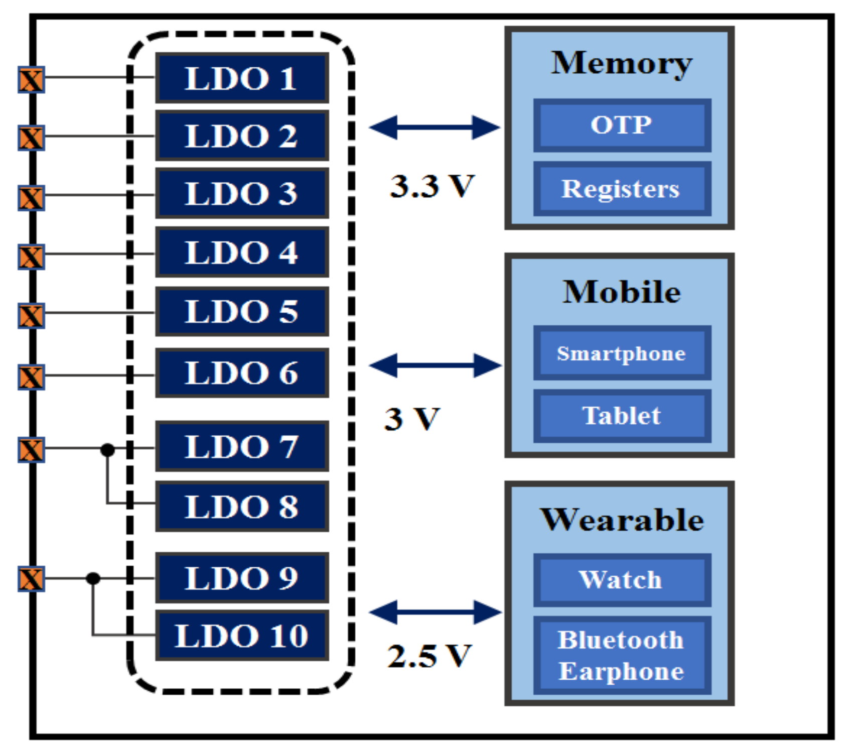
:1. Introduction
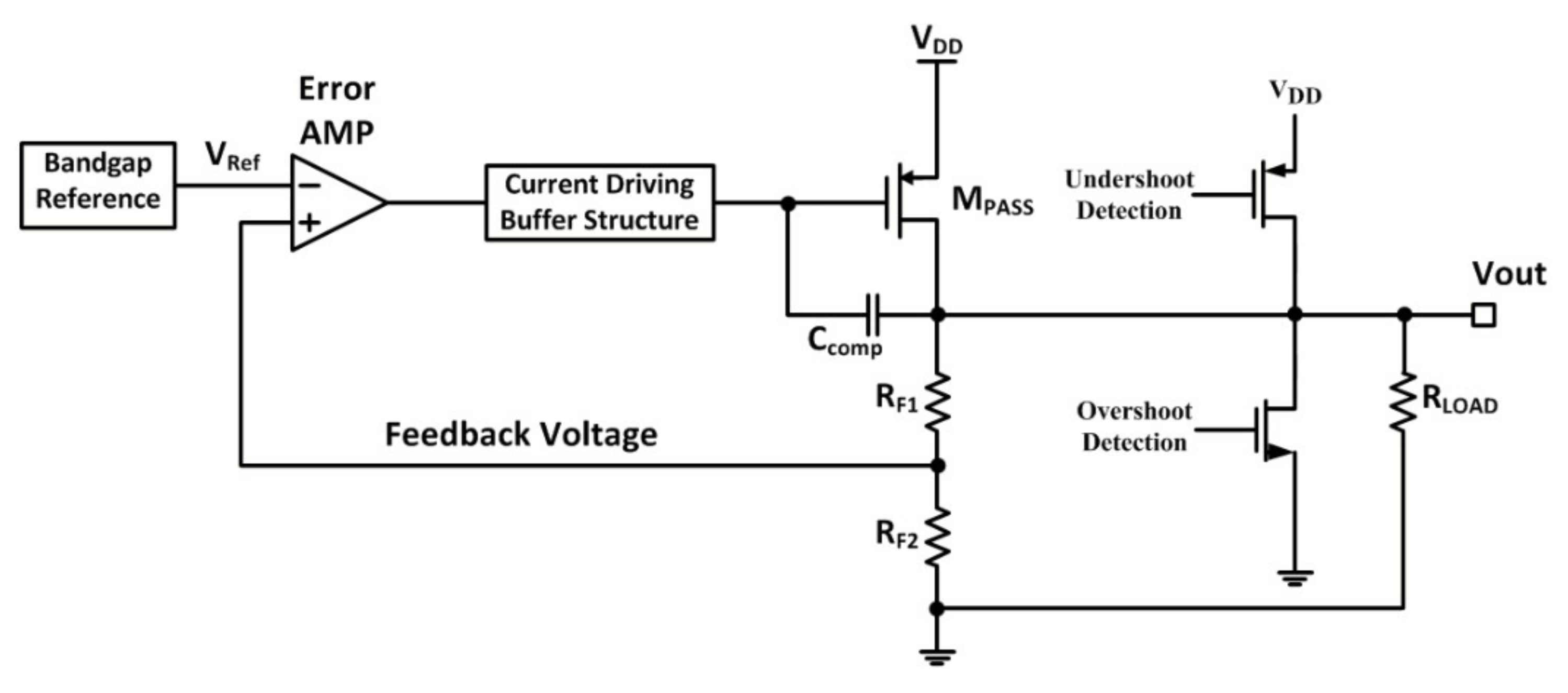
2. The Proposed LDO Regulator with ESD Protection Structure
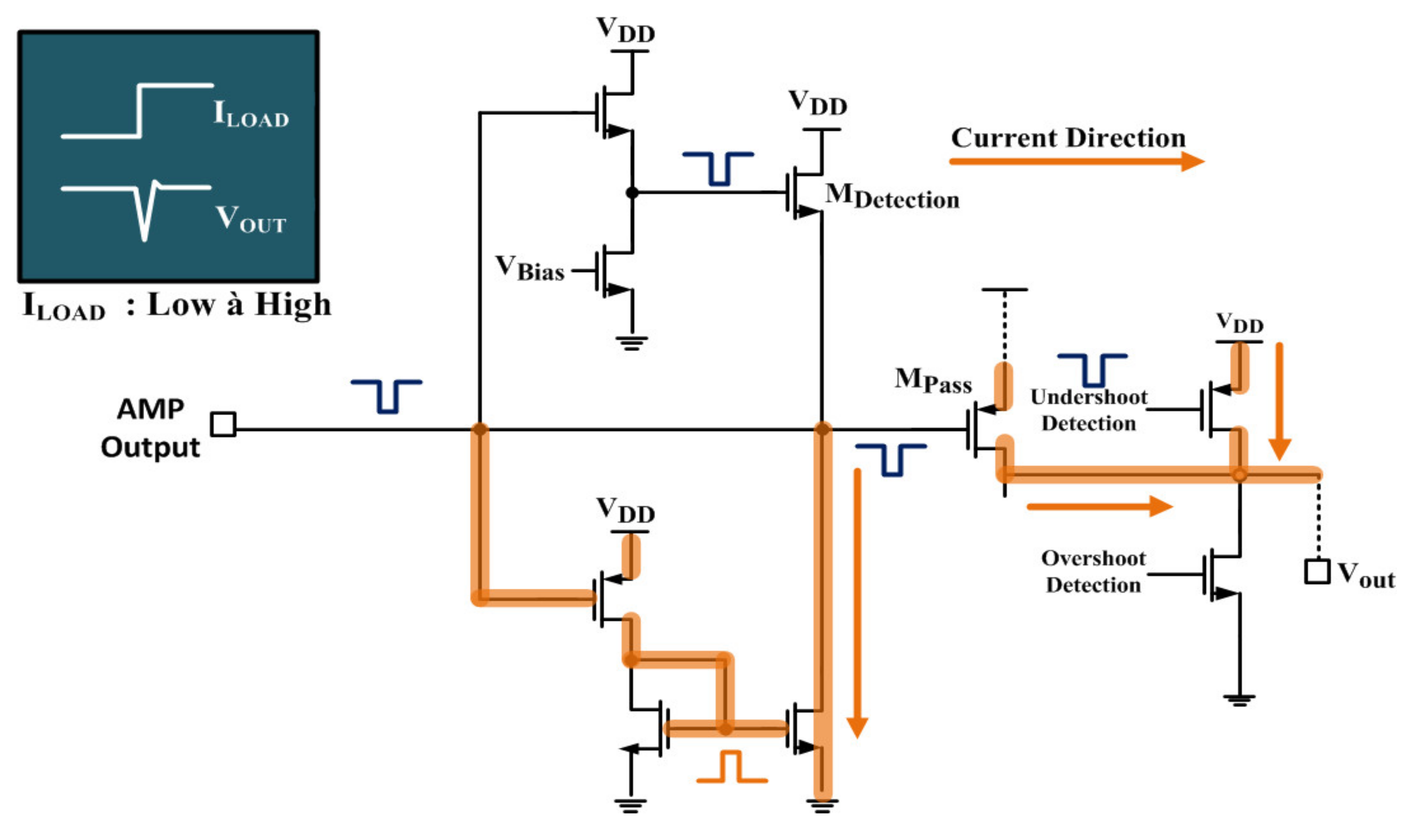
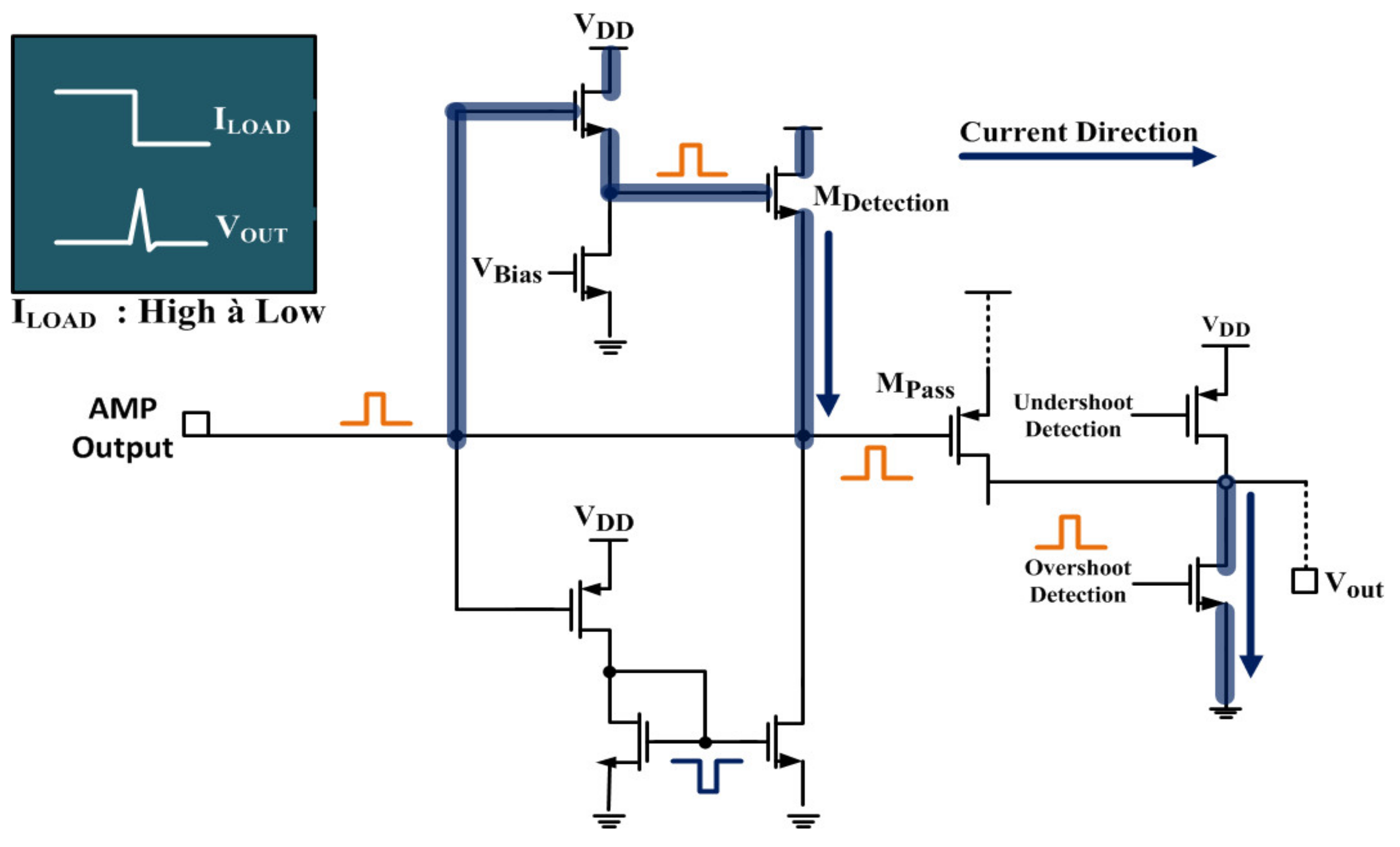
2.1. Current Driving Buffer Structure
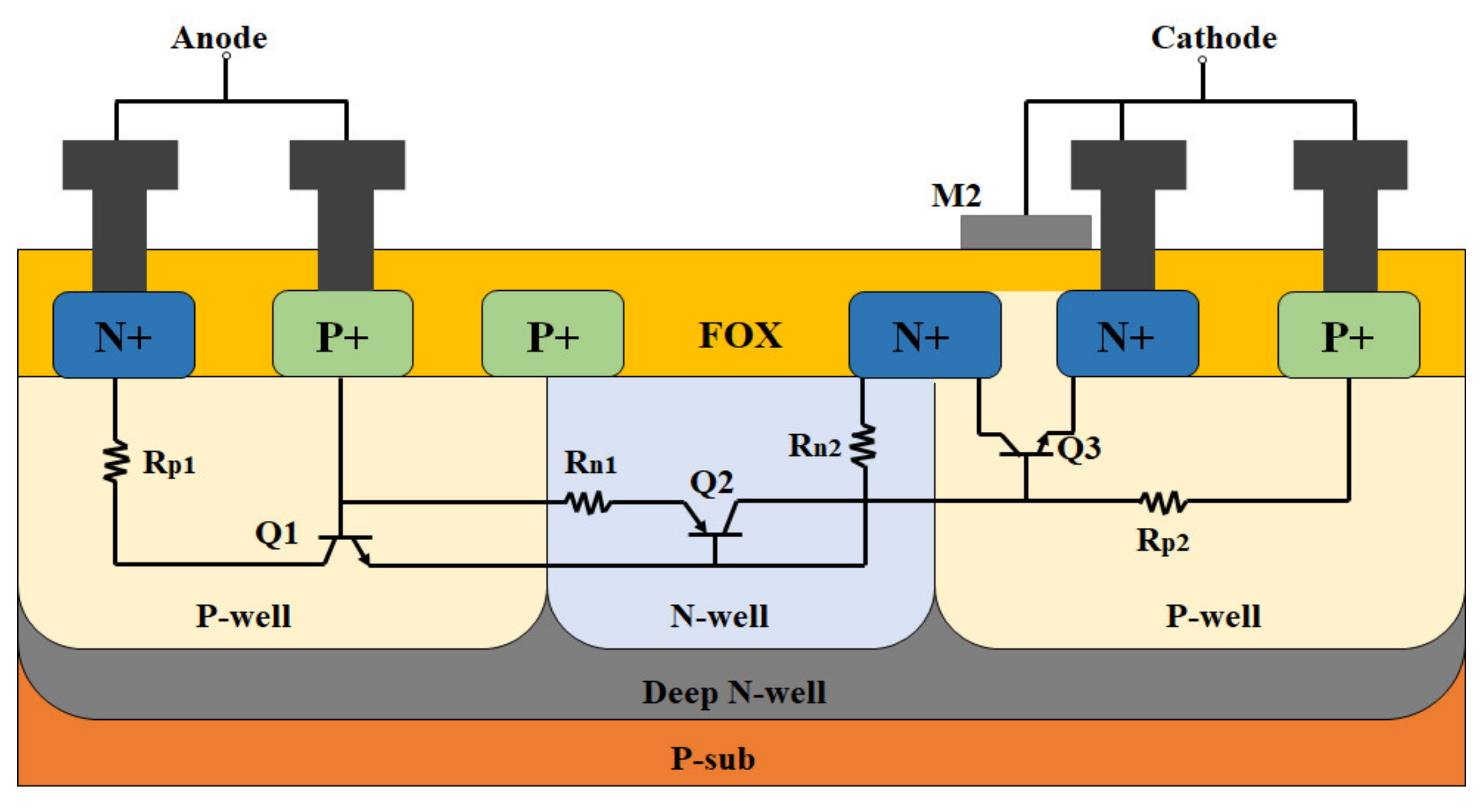
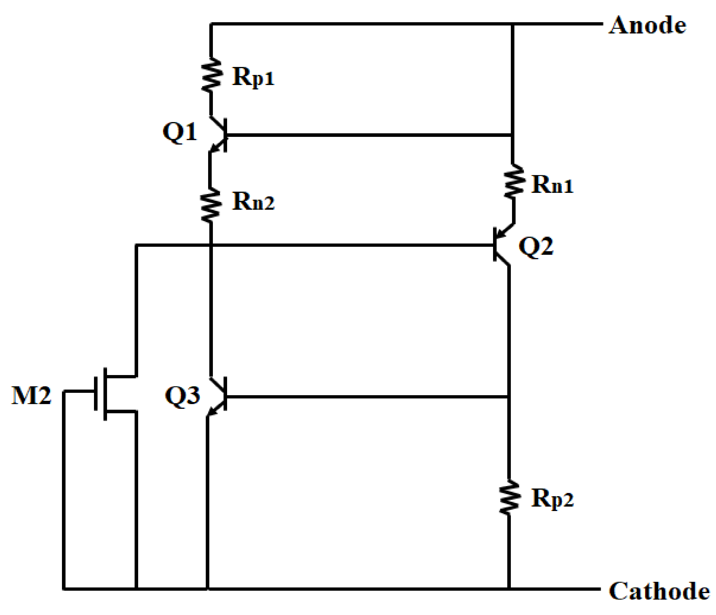
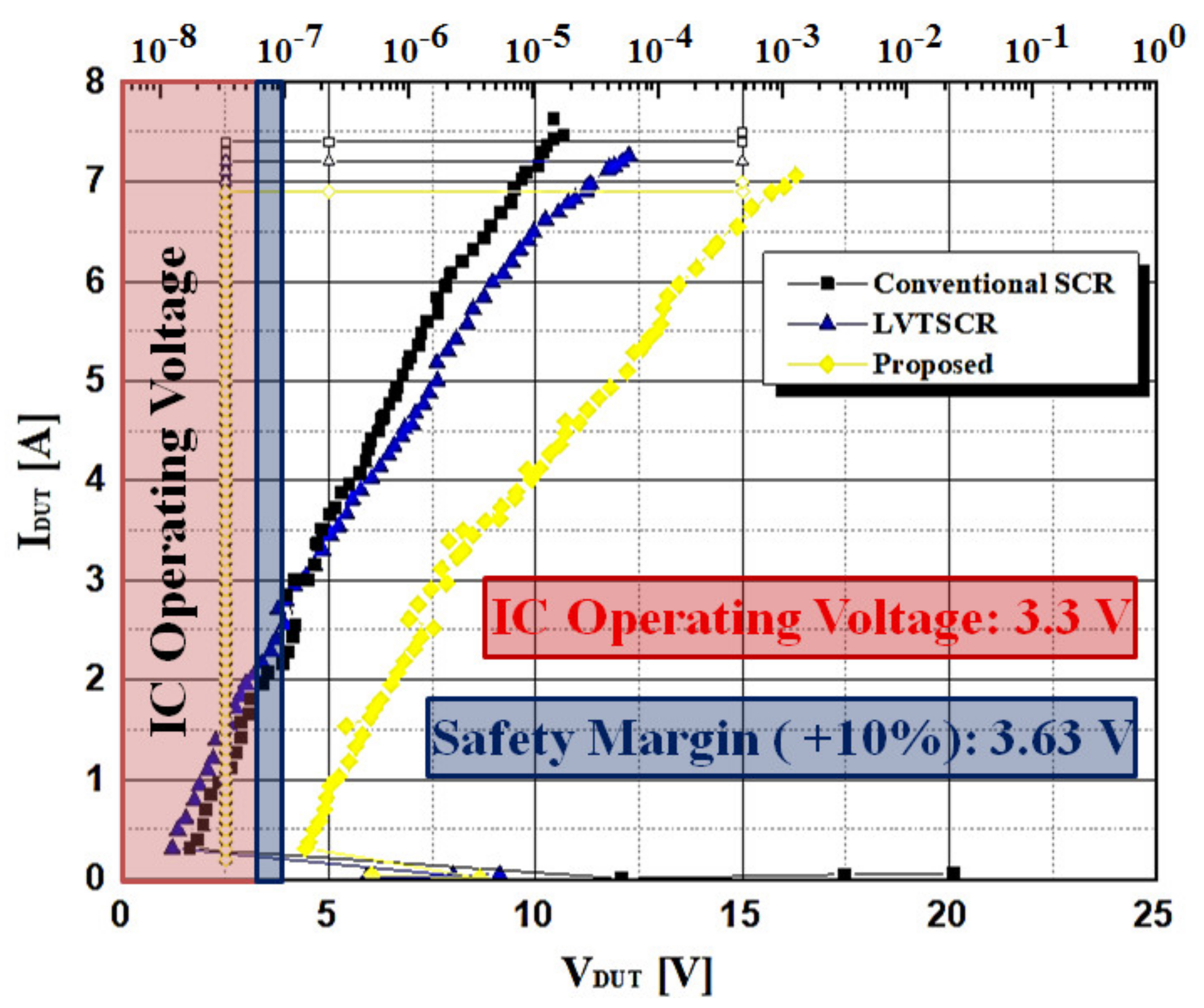
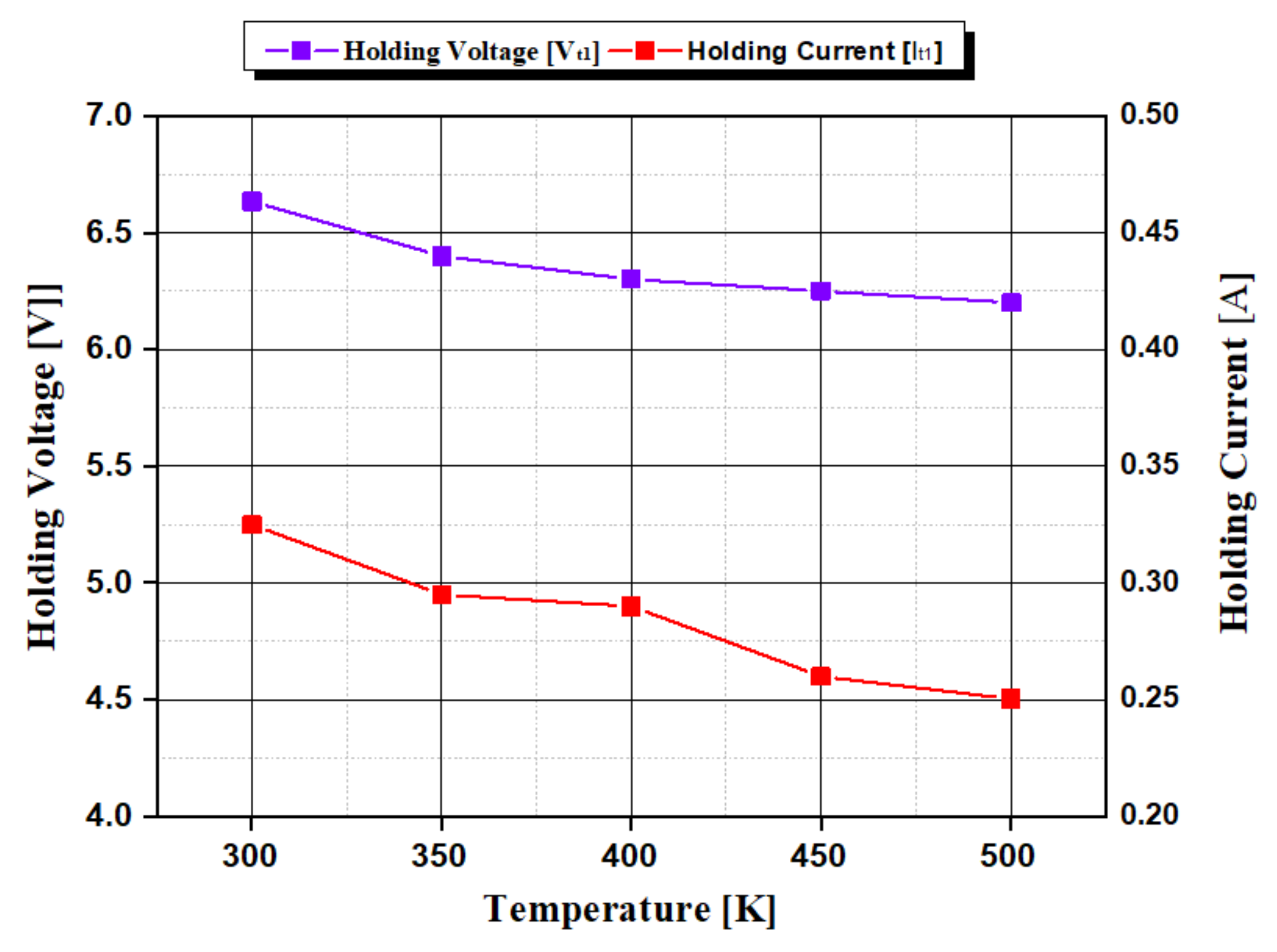
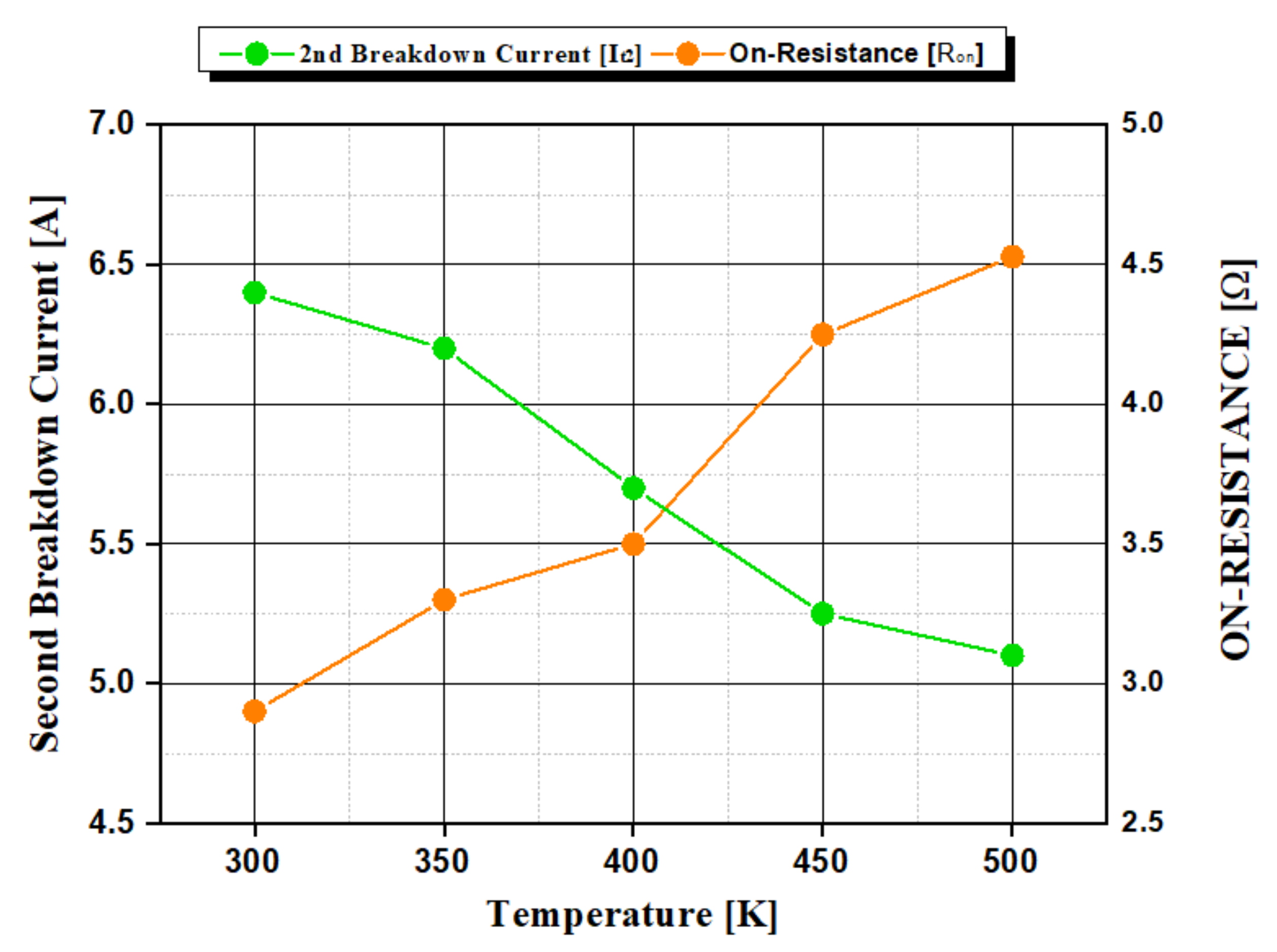
2.2. LVTSCR-Based ESD Protection Structure
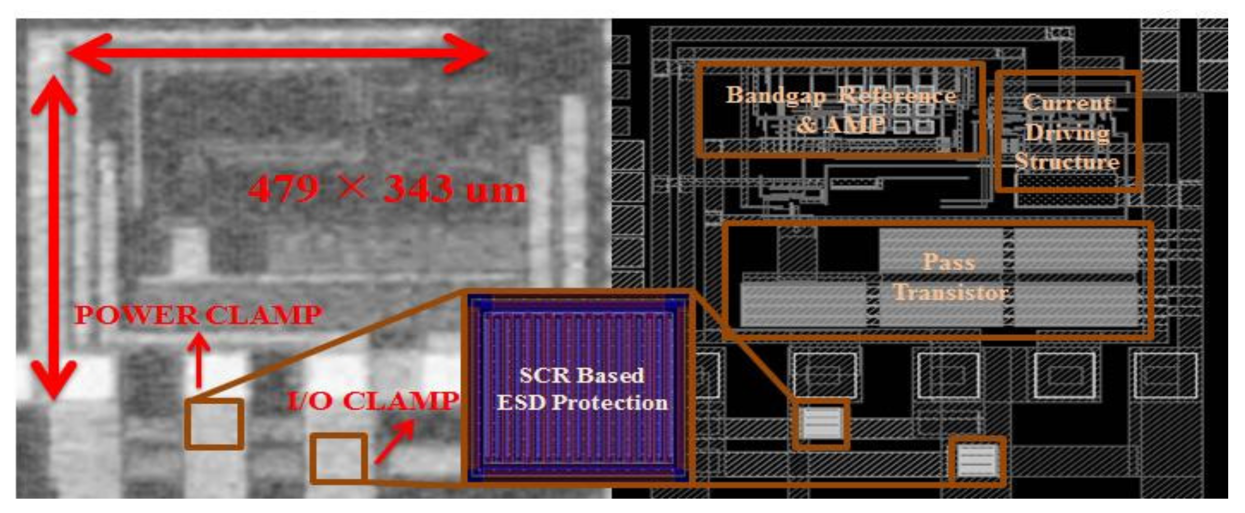
3. Simulation Result
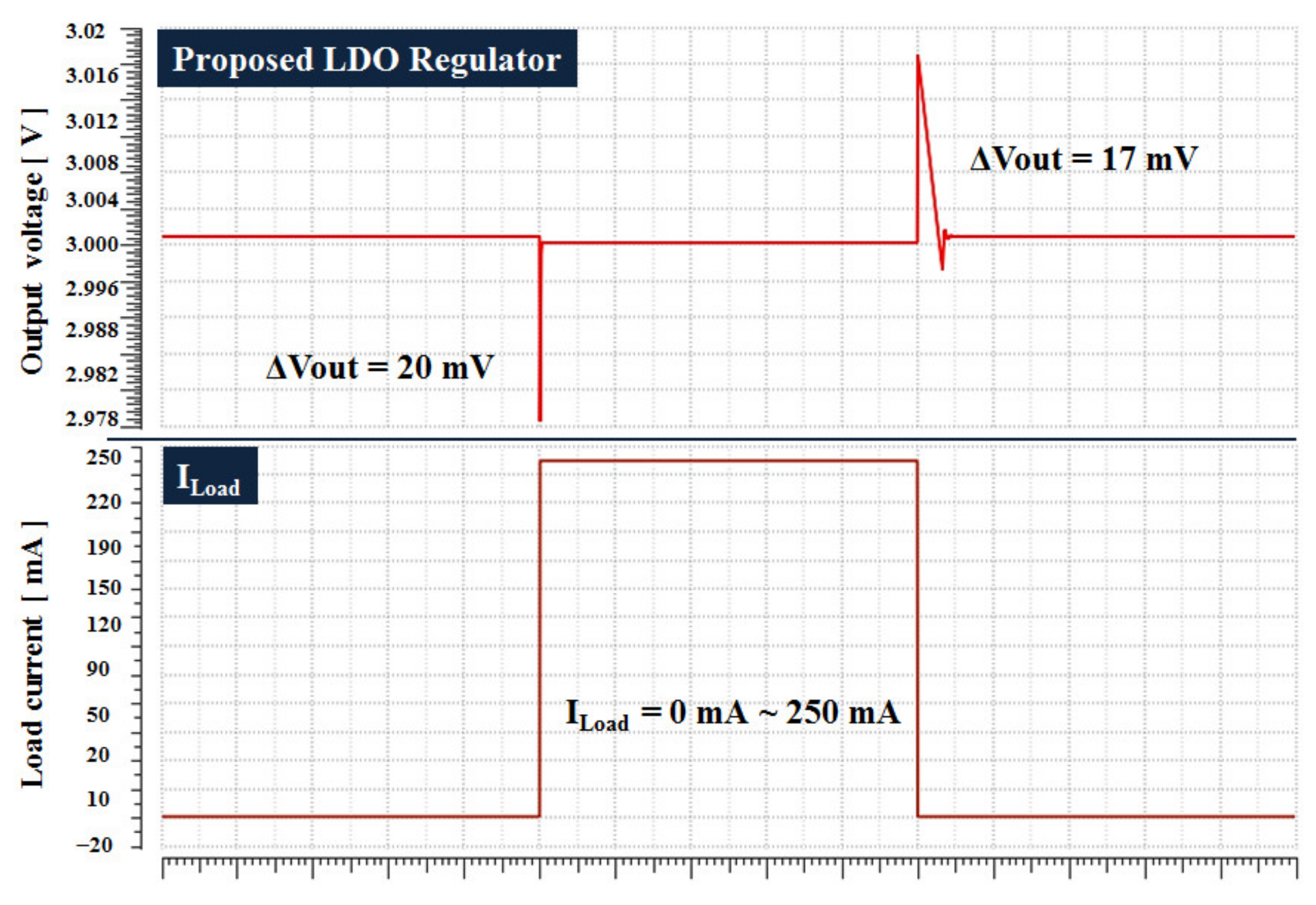
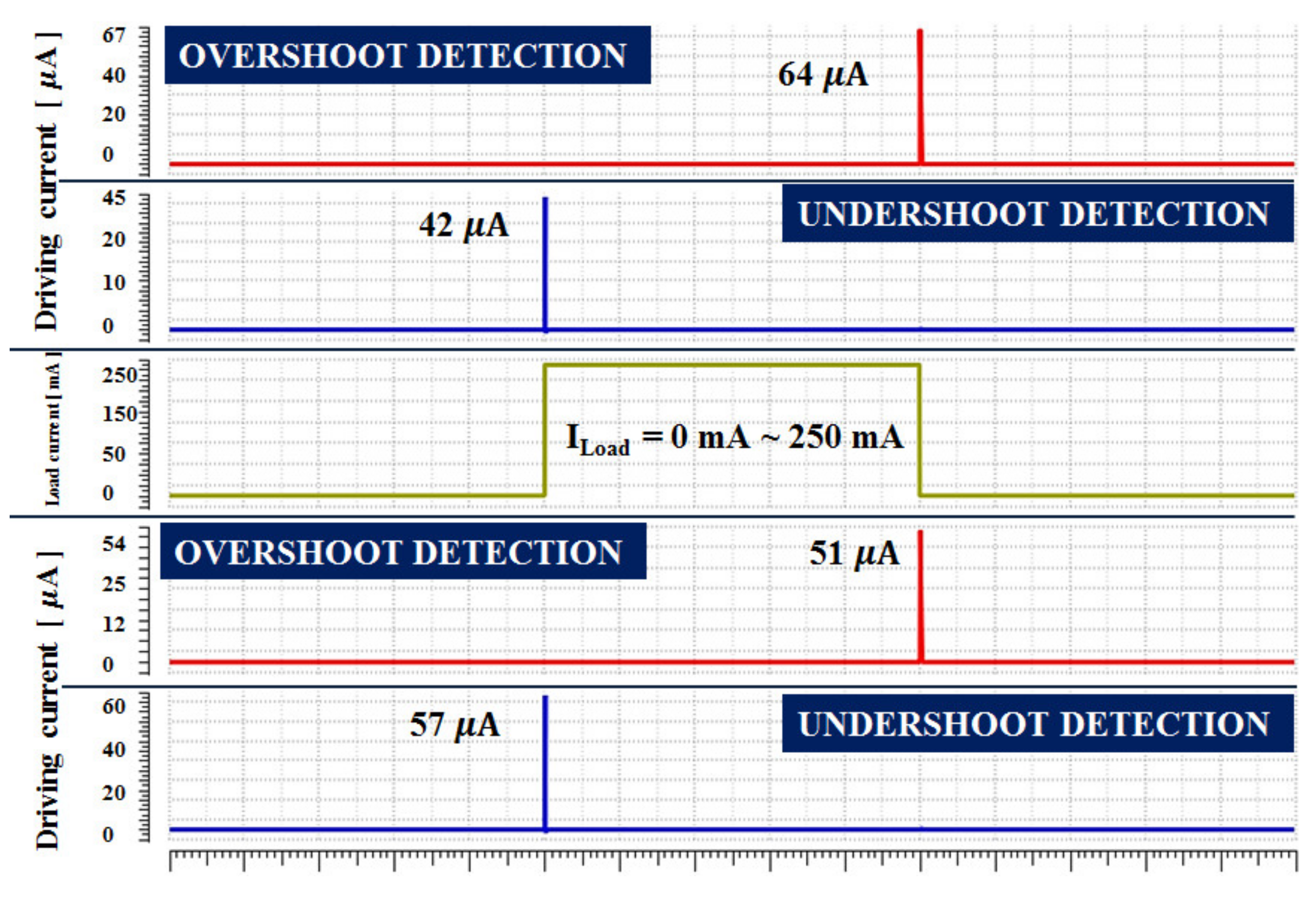
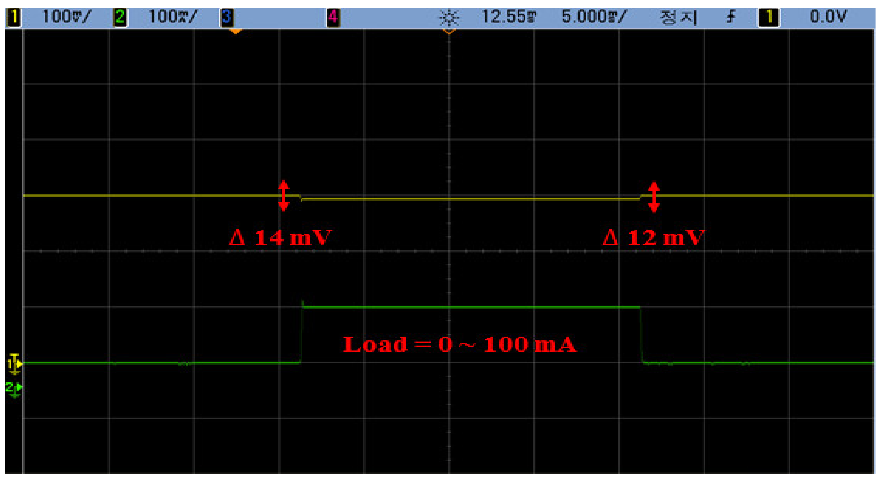
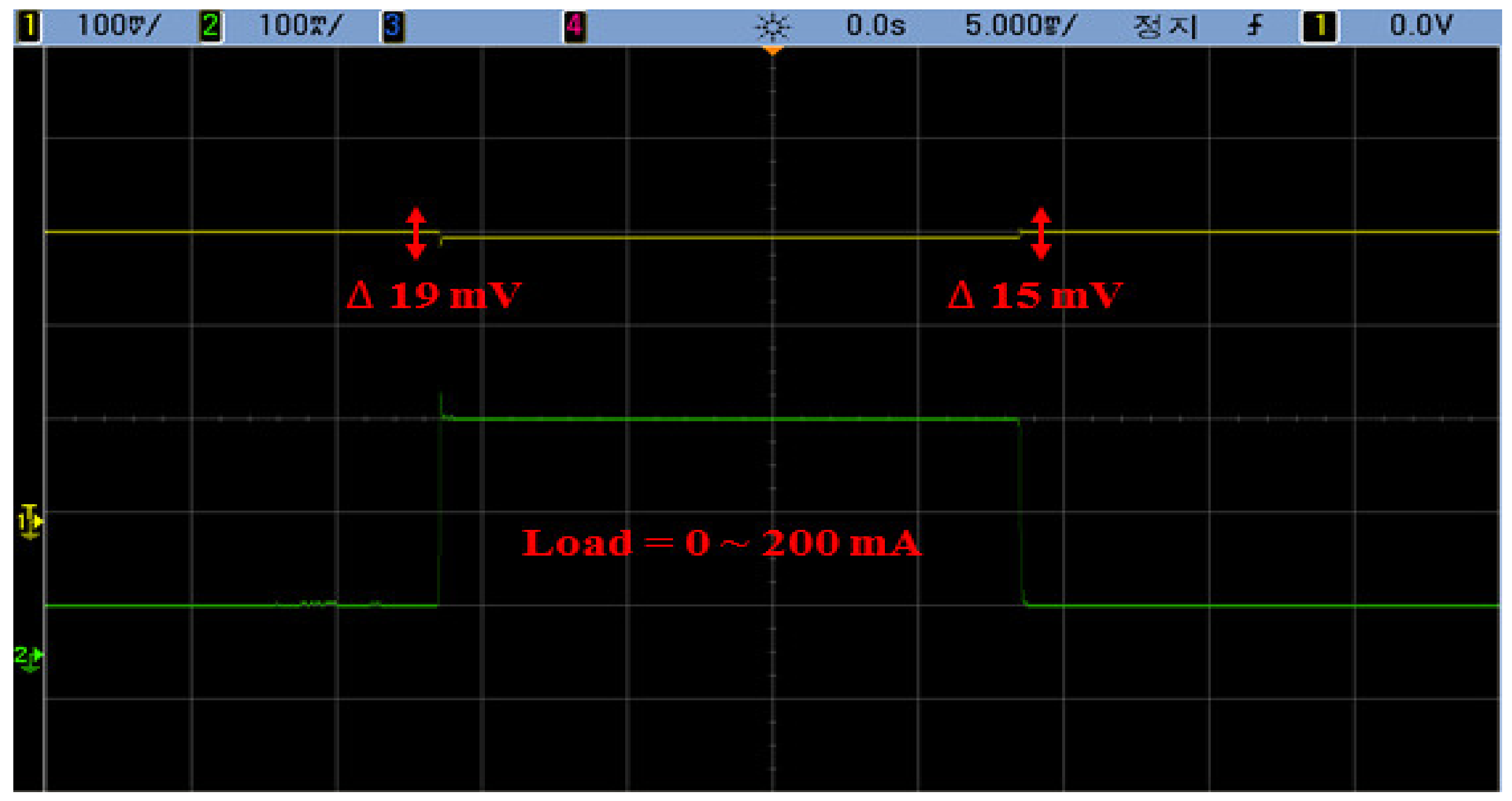
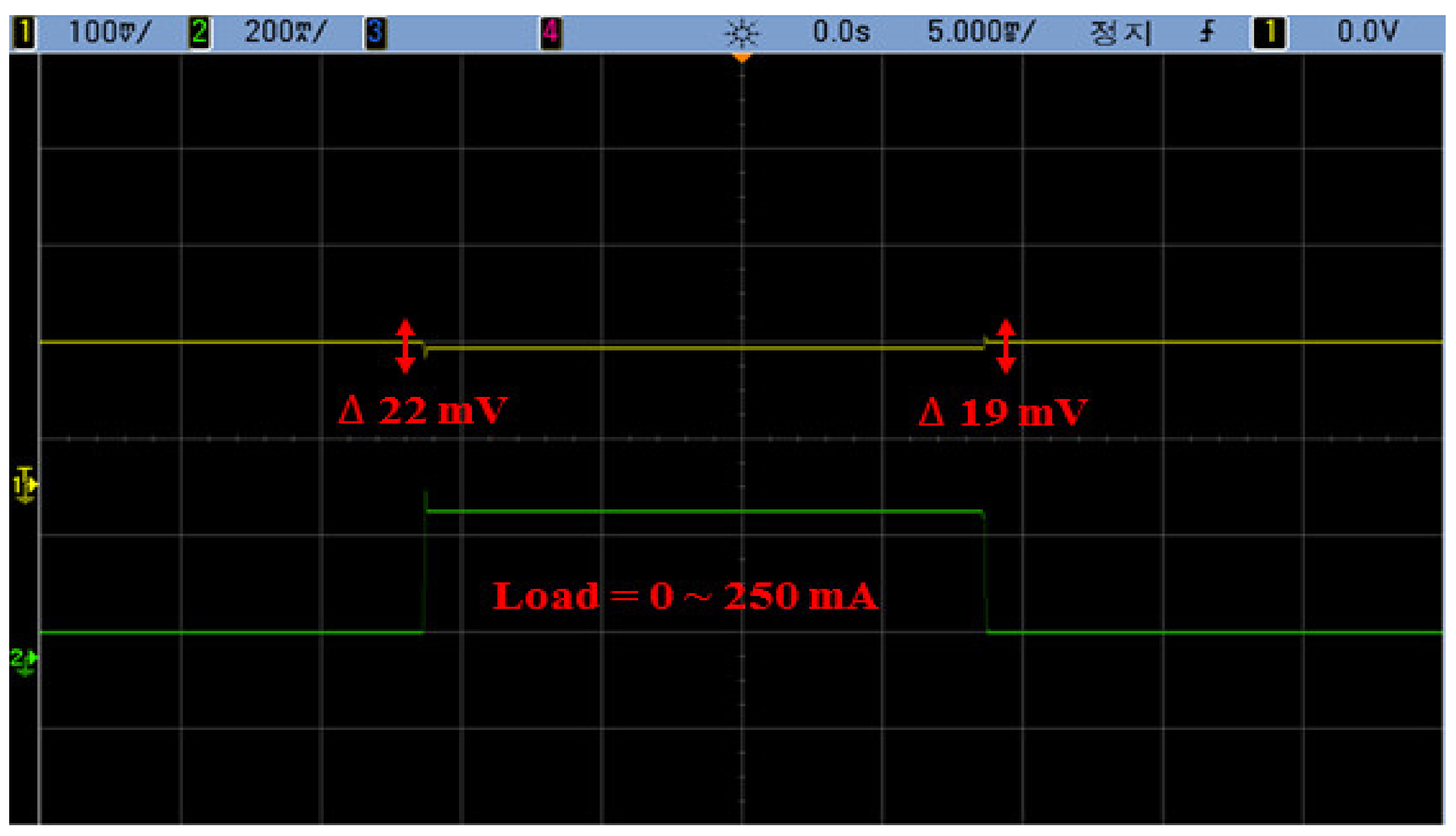
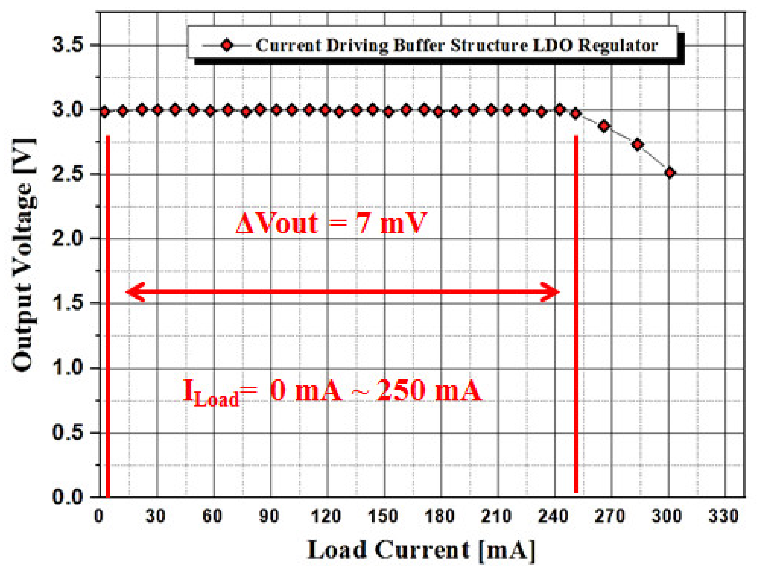
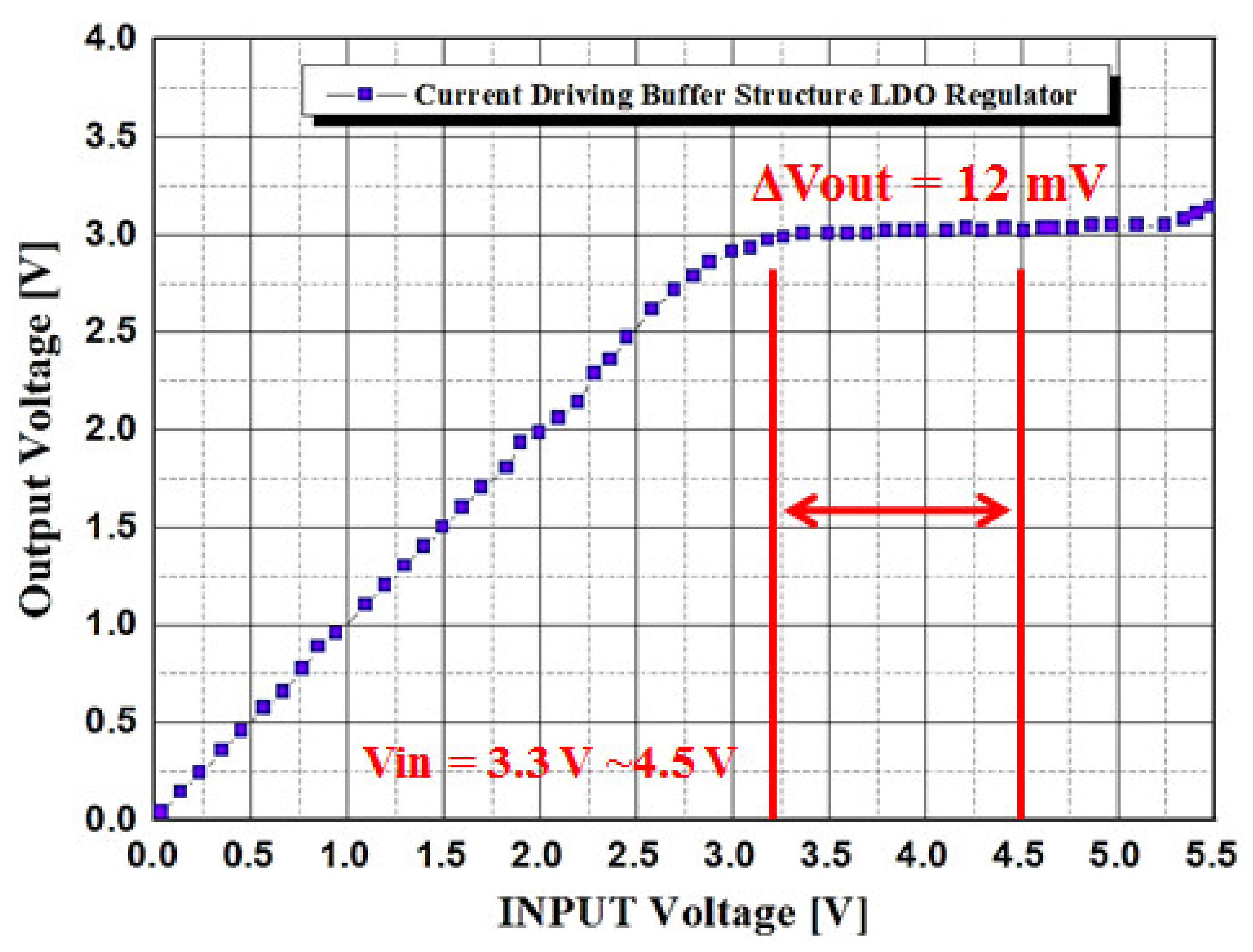
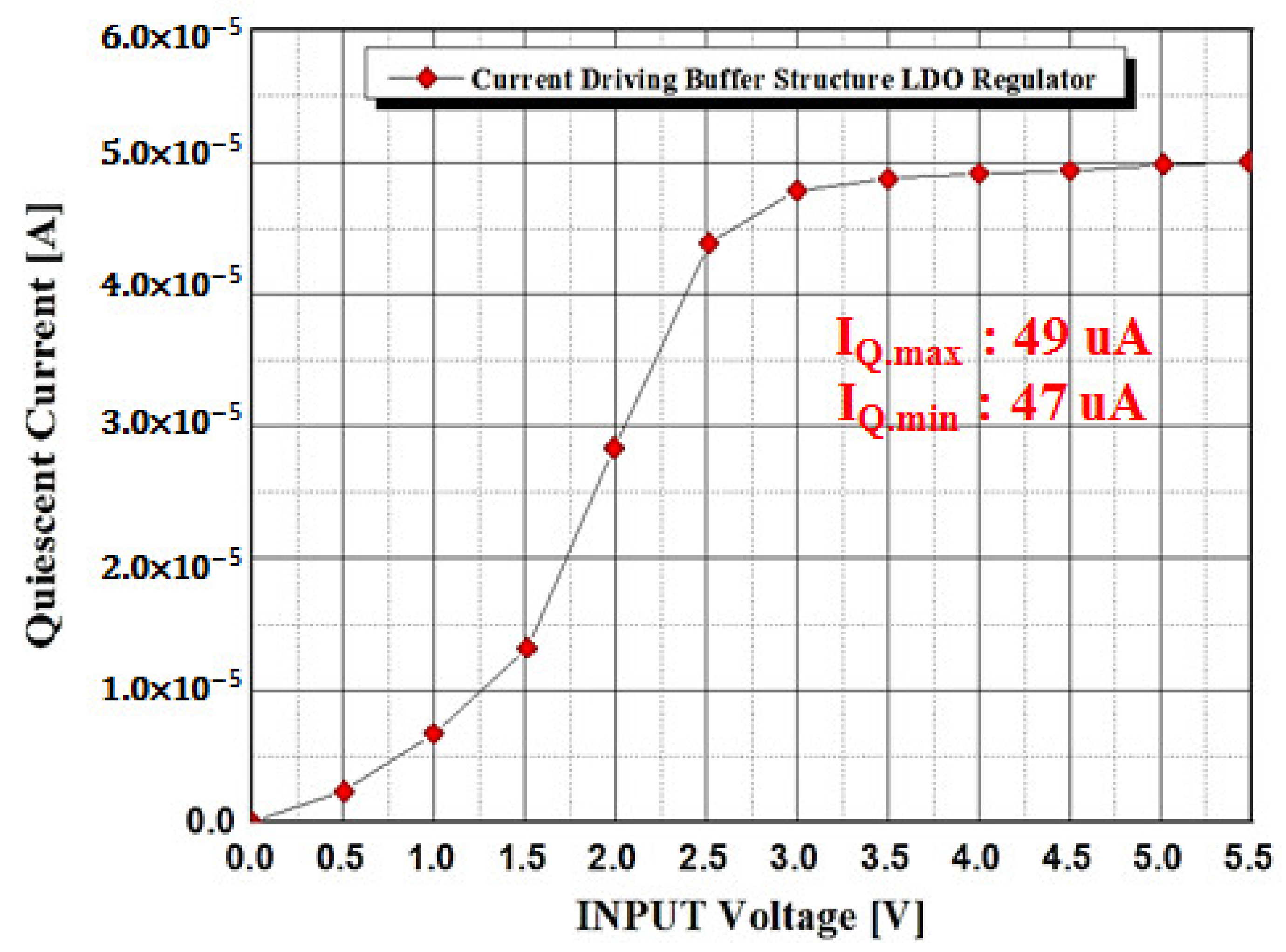
4. Measurement Result
5. Conclusions
Author Contributions
Funding
Data Availability Statement
Conflicts of Interest
References
- Moon, J.; Hyun, J.; Kim, S.-W. Design of low-power, fast-transient-response, capacitor-less low-dropout regulator for mobile applications. IEICE Electron. Express 2016, 13, 0882. [Google Scholar] [CrossRef] [Green Version]
- Koo, Y.S. A design of low-area low drop-out regulator using body bias technique. IEICE Electron. Express 2013, 10, 20130300. [Google Scholar] [CrossRef] [Green Version]
- Lau, S.K.; Mok, P.K.T.; Leung, K.N. A low-dropout regulator for SoC with Q-reduction. IEEE J. Solid-State Circuits 2007, 42, 658. [Google Scholar] [CrossRef]
- Jun, J.W.; Koo, Y.S.; Lee, K.Y. Design of high-reliability LDO with current limiting characteristics with built-in new high tolerance ESD protection circuit. IEICE Electron. Express 2013, 10, 20130516. [Google Scholar] [CrossRef] [Green Version]
- Manikandan, P.; Bindu, B. A transient enhanced cap-less low-dropout regulator for wide range of load currents and capacitances. Microelectron. J. 2021, 115, 105207. [Google Scholar] [CrossRef]
- Chong, S.S.; Chan, P.K. A 0.9-/spl mu/A Quiescent Current Output-Capacitorless LDO Regulator with Adaptive Power Transistors in 65-nm CMOS. IEEE Trans. Circuits Syst. I Regul. Pap. 2013, 60, 1072. [Google Scholar] [CrossRef]
- Wang, J.; Gao, D.; Hu-Guo, C.; Jaaskelainen, K.; Hu, Y. A High Load Current, Low-Noise, Area-Efficient, Full On-Chip Regulator for CMOS Pixel Sensors. IEEE Trans. Nucl. Sci. 2012, 59, 582. [Google Scholar] [CrossRef]
- Ming, X.; Li, Q.; Zhou, Z.K.; Zhang, B. An Ultrafast Adaptively Biased Capacitorless LDO With Dynamic Charging Control. IEEE Trans. Circuits Syst. II Express Briefs 2012, 59, 40–44. [Google Scholar] [CrossRef]
- Duan, Q.; Li, W.; Huang, S.; Ding, Y.; Meng, Z.; Shi, K. A Two-Module Linear Regulator with 3.9-10 V Input, 2.5 V Output, and 500 mA Load. Electronics 2019, 8, 1143. [Google Scholar] [CrossRef] [Green Version]
- Liu, N.; Chen, D. A Transient-Enhanced Output-Capacitorless LDO with Fast Local Loop and Overshoot Detection. IEEE Trans. Circuits Syst. I Regul. Pap. 2020, 67, 3422. [Google Scholar] [CrossRef]
- Han, W.; Lee, H. A 340-nA-Quiescent 80-mA-Load 0.02-fs-FOM Active-Capacitor-Based Low-Dropout Regulator in Standard 0.18-μm CMOS. IEEE Solid-State Circuits Lett. 2021, 125, 125–128. [Google Scholar] [CrossRef]
- Lavalle-Aviles, F.; Torres, J.; Sánchez-Sinencio, E. A High Power Supply Rejection and Fast Settling Time Capacitor-Less LDO. IEEE Trans. Power Electron. 2019, 34, 474–484. [Google Scholar] [CrossRef]
- Peng, S.-Y.; Liu, L.-H.; Chang, P.-K.; Wang, T.-Y.; Li, H.Y. A Power-Efficient Reconfigurable Output-Capacitor-Less Low-Drop-Out Regulator for Low-Power Analog Sensing Front-End. IEEE Trans. Circuits Syst. I Regul. Pap. 2017, 64, 1318. [Google Scholar] [CrossRef]
- Răducan, C.; Grăjdeanu, A.-T.; Plesa, C.-S.; Neag, M.; Negoiţă, A.; Ţopa, M.D. LDO With Improved Common Gate Class-AB OTA Handles any Load Capacitors and Provides Fast Response to Load Transients. IEEE Trans. Circuits Syst. I Regul. Pap. 2020, 37, 3740–3752. [Google Scholar] [CrossRef]
- Torres, J.; El-Nozahi, M.; Amer, A.; Gopalraju, S.; Abdullah, R.; Entesari, K.; Sanchez-Sinencio, E. Low Drop-Out Voltage Regulators: Capacitor-less Architecture Comparison. IEEE Circuits Syst. Mag. 2014, 14, 6. [Google Scholar] [CrossRef]
- Chen, J.J.; Yang, F.-C.; Kung, C.-M.; Lai, B.-P.; Hwang, Y.-S. A capacitor-free fast-transient-response LDO with dual-loop controlled paths. In Proceedings of the 2007 IEEE Asian Solid-State Circuits Conference, Jeju, Korea, 12–14 November 2007; Volume 12. [Google Scholar] [CrossRef]
- Park, K.-H.; Yang, I.-S.; Koo, Y.-S. A Design of Low-dropout Regulator with Adaptive Threshold Voltage Technique. J. Semicond. Technol. Sci. 2018, 18, 287. [Google Scholar] [CrossRef]
- Do, K.I.; Jin, S.-H.; Lee, B.-S.; Woo, J.-W.; Koo, Y.-S. Design of All-Directional ESD Protection circuit with SCR-based I/O and LIGBT-based Power clamp. In Proceedings of the 2021 International Conference on Electronics, Information, and Communication (ICEIC), Jeju, Korea, 31 January 2021–3 February 2021; p. 20533020. [Google Scholar] [CrossRef]
- Koo, Y.-S. Electrical characteristics of novel SCR - based ESD protection for power clamp. IEICE Electron. Express 2012, 9, 1479. [Google Scholar] [CrossRef] [Green Version]
- Do, K.I.; Koo, Y.-S. A Novel Low Dynamic Resistance Dual-Directional SCR With High Holding Voltage for 12 V Applications. IEEE J. Electron Devices Soc. 2020, 8, 635–639. [Google Scholar] [CrossRef]
- Do, K.I.; Jin, S.-H.; Lee, B.-S.; Koo, Y.-S. 4H-SiC-Based ESD Protection Design with Optimization of Segmented LIGBT for High-Voltage Applications. IEEE J. Electron Devices Soc. 2021, 9, 1017–1023. [Google Scholar] [CrossRef]
- Koo, Y.-S.; Lee, K.Y.; Kim, K.-D.; Kwon, J.-K. The design of high holding voltage SCR for whole-chip ESD protection. IEICE Electron. Express 2008, 5, 624. [Google Scholar] [CrossRef]
- Do, K.I.; Lee, B.; Kim, S.G.; Koo, Y.S. Design of 4H-SiC-Based Silicon-Controlled Rectifier with High Holding Voltage Using Segment Topology for High-Voltage ESD Protection. Electron Device Lett. 2020, 41, 1669–1672. [Google Scholar] [CrossRef]
- Koo, Y.-S.; Lee, K.-Y. SCR-based ESD protection device with low trigger and high robustness for I/O clamp. IEICE Electron. Express 2012, 9, 200. [Google Scholar] [CrossRef] [Green Version]
- Do, K.I.; Song, B.-B.; Koo, Y.S. A Gate-Grounded NMOS-Based Dual-Directional ESD Protection with High Holding Voltage for 12 V Application. IEEE Trans. Device Mater. Reliab. 2020, 20, 716–722. [Google Scholar] [CrossRef]
- Do, K.I.; Koo, Y.S. Silicon-controlled Rectifier-based Electrostatic Discharge Protection Circuit with Additional NPN Parasitic Bipolar Junction Transistor for 5-V Application. J. Semicond. Technol. Sci. 2021, 21, 101. [Google Scholar] [CrossRef]
- Koo, Y.-S. Analysis of the electrical characteristics of SCR-based ESD Protection Device (PTSCR) in 0.13/0.18/0.35um process technology. IEICE Electron. Express 2011, 8, 8. [Google Scholar] [CrossRef] [Green Version]
- Do, K.I.; Lee, B.-S.; Koo, Y.-S. A New Dual-Direction SCR With High Holding Voltage and Low Dynamic Resistance for 5 V Application. IEEE J. Electron Devices Soc. 2019, 7, 601–605. [Google Scholar] [CrossRef]
- Do, K.I.; Lee, B.-S.; Koo, Y.-S. Study on 4H-SiC GGNMOS Based ESD Protection Circuit with Low Trigger Voltage Using Gate-Body Floating Technique for 70-V Applications. IEEE Electron Device Lett. 2019, 40, 283–286. [Google Scholar] [CrossRef]
- Song, B.-B.; Do, K.-I.; Koo, Y.S. SCR-Based ESD Protection Using a Penta-Well for 5 V Applications. IEEE J. Electron Devices Soc. 2018, 6, 691–695. [Google Scholar] [CrossRef]
- Do, K.I.; Song, B.-B.; Koo, Y.S. A Novel Dual-Directional SCR Structure with High Holding Voltage for 12-V Applications in 0.13-μm BCD Process. IEEE Trans. Electron Devices 2020, 67, 5020–5027. [Google Scholar] [CrossRef]
- Song, B.-B.; Lee, B.-S.; Yang, I.-S.; Koo, Y.-S. Analysis of a Parasitic-Diode-Triggered Electrostatic Discharge Protection Circuit for 12 V Applications. ETRI J. 2017, 39, 746–755. [Google Scholar] [CrossRef] [Green Version]
- Do, K.I.; Koo, Y.S. A New SCR Structure with High Holding Voltage and Low ON-Resistance for 5-V Applications. IEEE Trans. Electron Devices 2020, 67, 1052–1058. [Google Scholar] [CrossRef]
- Do, K.I.; Lee, B.-S.; Chae, H.-G.; Seo, J.-J.; Koo, Y.S. A Novel Low Trigger SCR with Latch up Immunity for 5 V Application. In Proceedings of the European Conference on Electrical Engineering and Computer Science (EECS), Bern Switzerland, 20–22 December 2018. [Google Scholar] [CrossRef]
- Do, K.I.; Won, J.-I.; Koo, Y.S. A 4H-SiC MOSFET-Based ESD Protection with Improved Snapback Characteristics for High-Voltage Applications. IEEE Trans. Power Electron. 2021, 36, 4921–4926. [Google Scholar] [CrossRef]


| Measurement | [1] | [2] | [3] | [7] | [8] | [12] | [14] | This Work |
|---|---|---|---|---|---|---|---|---|
| Technology (μm) | 0.35 | 0.13 | 0.35 | 0.35 | 0.35 | 0.13 | 0.13 | 0.18 |
| Supply Voltage(V) | 3.3 | 2.7 | 1.2 | 3.3 | 2.5 | 1.2 | 1.2 | 3.3 |
| Output Voltage (V) | 2.9 | 2.5 | 1 | 3 | 2.35 | 1 | 1 | 3 |
| Load Current: IMAX (mA) | 100 | 100 | 100 | 200 | 100 | 50 | 100 | 250 |
| Quiescent Current (µA) | 55 | 72 | - | 147 | 7 | 42 | 0.7 | 49 |
| Load Transient (ILOAD Rising) (mV) | 90 | - | 45 | 100 | 236 | 140 | 76 | 22 |
| Load Transient (ILOAD Falling) (mV) | 160 | - | 42 | 110 | 227 | 80 | 198 | 19 |
| Load Regulation (mV) | - | 100 | 4.2 | 45 | 8 | 10 | 10 | 7 |
| Line Regulation (mV) | - | 20 | 3 | 34 | 1 | 30 | 16.6 | 12 |
| COUT (pF) | 100 | 2.2 × 10⁶ | 100 | 1 × 10⁶ | 0–100 | 400 | 0–1 × 10⁶ | 100 |
| Year | 2016 | 2013 | 2007 | 2010 | 2020 | 2019 | 2020 | 2022 |
Publisher’s Note: MDPI stays neutral with regard to jurisdictional claims in published maps and institutional affiliations. |
© 2022 by the authors. Licensee MDPI, Basel, Switzerland. This article is an open access article distributed under the terms and conditions of the Creative Commons Attribution (CC BY) license (https://creativecommons.org/licenses/by/4.0/).
Share and Cite
Kwon, S.-W.; Koo, Y.-S. Design of Capacitor-Less High Reliability LDO Regulator with LVTSCR Based ESD Protection Circuit Using Current Driving Buffer Structure. Electronics 2022, 11, 1781. https://doi.org/10.3390/electronics11111781
Kwon S-W, Koo Y-S. Design of Capacitor-Less High Reliability LDO Regulator with LVTSCR Based ESD Protection Circuit Using Current Driving Buffer Structure. Electronics. 2022; 11(11):1781. https://doi.org/10.3390/electronics11111781
Chicago/Turabian StyleKwon, Sang-Wook, and Yong-Seo Koo. 2022. "Design of Capacitor-Less High Reliability LDO Regulator with LVTSCR Based ESD Protection Circuit Using Current Driving Buffer Structure" Electronics 11, no. 11: 1781. https://doi.org/10.3390/electronics11111781