1. Introduction
Three-level converter topologies, especially in combination with wide-bandgap (WBG) power semiconductors such as SiC MOSFETs, are enabling ever more compact and more efficient power electronic converter systems [
1,
2,
3,
4], and are therefore of key importance to next-generation PFC rectifiers for battery charging, datacenter power supply modules, and inverter systems for variable-speed drives used in industry automation and electrified transport. In particular, the three-level T-type (3LTT) converter (cf.,
Figure 1), originally proposed in the 1970s [
5], achieves very promising performance for 800 V DC-link applications, especially if modern WBG power semiconductors are employed [
3,
6]. Essentially, a two-level bridge-leg (with 1200 V SiC MOSFETs) is extended by a four-quadrant switch that allows the connection of the AC output terminal to the DC-link midpoint, i.e., enables three output voltage levels. The four-quadrant midpoint switch can advantageously be realized with two 650 V SiC MOSFETs connected in anti-series. Compared to other three-level topologies, such as the neutral-point-clamped (NPC) converter [
7,
8], or its sibling with active switches instead of clamping diodes (active NPC, ANPC) [
9], the 3LTT requires, thus, fewer power semiconductors and, especially, fewer gate-drive power supplies (if the midpoint switch employs a common-source configuration); i.e., the 3LTT shows a favorable trade-off between functionality and complexity [
10].
To perform a first-step comparative evaluation of different power semiconductors for a given application, there is a need to quickly estimate switching losses. Whereas datasheets usually directly provide turn-on and turn-off energy losses as a function of voltage and current for symmetric two-level bridge-legs, the situation is more complicated for 3LTT bridge-legs [
6,
11]. First, any commutation between two semiconductor devices also changes the blocking voltage across a third device connected to the common switching node, causing additional capacitive losses. Second, the commutations occur between semiconductors with different blocking voltage and/or current ratings (i.e., for the example mentioned above, between a 1200 V SiC MOSFET and a 650 V SiC MOSFET used as the midpoint switch). For these reasons, it is not possible to use the switching loss data available in typical semiconductor datasheets directly for estimating the switching losses of a certain device combination in a 3LTT bridge-leg.
Therefore, this paper provides a simplified approach to estimate the minimum hard-switching losses of SiC-MOSFET-based 3LTT bridge-legs by considering only charge-related losses (i.e., capacitive and reverse-recovery losses), which effectively dominate the hard-switching energy loss for fast-switching power semiconductors [
12]. This paper consolidates existing contributions to semiconductor output capacitance charge/discharge loss modeling for three-level bridge-legs [
6,
11,
13], as well as to the simplified estimation of diode reverse-recovery losses [
6,
11], into a compact, straightforward loss modeling approach.
In contrast to the interesting switching loss estimation method developed in [
13], which requires double-pulse test loss measurement results, the loss model proposed herein can be parametrized with datasheet information on the devices’ output capacitances,
Coss, and reverse-recovery charge,
Qrr, only. Additionally, targeting GaN devices, the modeling approach outlined in [
13] does not account for reverse-recovery losses, i.e., it is not directly applicable to 3LTT bridge-legs with SiC MOSFETs. The switching-loss model in [
13] has only been verified indirectly at the converter level by measuring the total converter losses of a 3LTT undiriectional rectifier adopting 650 V GaN HEMTs and 1200 V SiC Schottky diodes.
In this paper, a dedicated experimental verification of the proposed loss model is performed on an 800 V DC-link 3LTT bridge-leg prototype (using 1200 V and 650 V SiC MOSFETs) through accurate calorimetric loss measurements. The experimental results confirm an almost perfect prediction of capacitive charge/discharge losses and show that the proposed model, including diode reverse-recovery, achieves a maximum hard-switching loss underestimation error of 18% (i.e., due to neglecting overlap losses [
12]). It is worth highlighting that even though this work focuses on the 3LTT converter topology (for reasons of clarity and conciseness), the proposed hard-switching-loss model can be applied to arbitrary three-level bridge-legs (e.g., NPC, ANPC, etc.), as explained in [
6].
The paper is organized as follows. First,
Section 2 discusses the modeling of capacitive losses in a 3LTT bridge-leg, clarifying also the impact of the third device connected to the switching node but not actively involved in the commutation. In
Section 3, a simplified model for the estimation of the bridge-leg losses in hard-switching operation is described, taking into account both capacitive and reverse-recovery loss contributions.
Section 4 provides a direct experimental verification of the proposed models, using highly accurate calorimetric measurements of the semiconductor losses. Finally,
Section 5 concludes the paper and gives an outlook on future developments, highlighting the importance of comprehensive reverse-recovery information in device datasheets.
2. Three-Level T-Type Capacitive Loss Analysis
This section provides a detailed analysis of the losses related to the charging/discharging of the semiconductor output capacitances in a 3LTT bridge-leg, as shown in
Figure 1. In particular, this analysis focuses only on the upper half of the bridge-leg (i.e.,
switching transitions, cf.,
Figure 1), since all results can be extended directly to the other bridge-leg half for reasons of symmetry. According to
Figure 1, four different switching events can occur, depending on the commutation sequence (i.e.,
or
) and the direction of the bridge-leg output current
. For each situation, the respective figure shows the steady state before the transition or the dead time interval, the transition interval (only for hard-switching events), and the steady state after the transition.
For example,
Figure 1a shows a transition from
to
(
) with
. In the initial steady state (not shown), the switching node is connected to the DC-link midpoint via
and
. The dead time interval starts when
turns off. During this interval, the switching node voltage does not change, as the load current flows in
’s body diode until
turns on. This turn-on process dissipates the energy
stored in the output capacitance of
, and causes the indicated current flows to charge the output capacitance of
to
and to charge
’s output capacitance from
to
. The turn-on process of
also initiates the reverse-recovery process of
’s body diode, which is discussed in
Section 3. Finally, in the new steady state, the switching node is connected to the positive DC-link rail via
. Since a certain amount of energy is always dissipated during the switching transition (e.g.,
), this is considered a hard-switching event. Similarly,
Figure 1b shows the transition in the opposite direction, i.e., from
to
(
) with
. Once
turns off, the load current charges/discharges the involved output capacitances until the switching node is finally connected to the DC-link midpoint via
and
’s body diode. The turn-on of
at the end of the dead time interval is, thus, lossless, and accordingly, this transition is a soft-switching event. The transitions in
Figure 1c,d follow analogous steps.
The indicated charging/discharging currents give rise to losses. To quantify these capacitive switching losses, all four switching events shown in
Figure 1 are analyzed using the method reported in [
14], which is based on the energy balance expression
where
and
are the total stored energies in all device capacitances before and after the commutation, respectively, while
and
are the energies provided by the DC-link and absorbed by the output load during the transition, respectively. Note that instantaneous switching transitions are assumed (i.e., no
V-
I overlap across the MOSFET channel); hence, no energy is transferred to the load during the hard-switching events (a) and (c) (i.e.,
), whereas no loss is generated during the soft-switching events (b) and (d) (i.e.,
, assuming a sufficient dead time to complete the voltage transition [
14]). Therefore, the energy balance terms for the two hard-switching events (a) and (c) are derived as
where
and
refer to the charge and the energy stored in the semiconductor output capacitance
, respectively:
For reasons of clarity and compactness, we define the energy terms
which are graphically illustrated in
Figure 2 for a Wolfspeed 1200 V 32 mΩ SiC MOSFET and
Vdc = 800 V. By inserting Equations (
2) and (
3) in Equation (
1) and leveraging Equations (
5)–(
8), straightforward capacitive loss expressions are obtained:
Note that different expressions are obtained for
and
, as the power semiconductors involved in the respective commutations are different (i.e.,
; for example, in a bridge-leg with 800 V DC-link voltage,
is typically a 1200 V MOSFET, whereas
is typically a 650 V MOSFET) and the charging/discharging of
(i.e., the output capacitance of the third power semiconductor not actively involved in the commutation) is affected by the current direction, as it is
charged from
to
in the hard-switching transition with
, shown in
Figure 1a, but
discharged from
to
in the hard-switching transition with
, shown in
Figure 1c.
3. Simplified Hard-Switching Loss Model
The total losses generated by a hard-switching commutation in an arbitrary SiC MOSFET bridge-leg can be expressed as [
12]
where
and
are the switched voltage and current, respectively,
is the capacitive loss contribution (depending on the switched voltage and the direction of the switched current, cf., Equations (
9) and (
10) in
Section 2, and
is the reverse-recovery charge of the MOSFET body diode involved in the commutation process (e.g., the body diode of
in
Figure 1a and the body diode of
in
Figure 1c). The last two terms of Equation (
11) represent the
V-
I overlap losses and depend on the voltage and current time derivatives during the overlap time. It is worth noting that Equation (
11) only represents turn-on losses, as the switching losses during the turn-off transition can typically be neglected if the MOSFET is assumed to be turned off fast enough [
12].
A simplified switching-loss model, only accounting for the unavoidable charge-related losses [
6,
11], can be obtained by assuming infinitely fast transitions, such that the
V-
I overlap loss contributions in Equation (
11) can be neglected. This assumption also allows to express the diode reverse-recovery charge as a linear function of the switched current [
15]: infinitely fast current transitions force the complete diode forward bias injected charge (which is proportional to the conducted current) to be swept away as
, because no time is left for charge recombination to take place. Thus, we obtain
where
is the charge carrier recombination lifetime. Therefore, a simplified linear switching-loss model with respect to the switched current is obtained from Equation (
11) as
which represents a theoretical lower limit (as overlap losses are neglected) for hard-switching losses in arbitrary SiC MOSFET bridge-legs.
Remarkably, Equation (
13) solely depends on typically available manufacturer datasheet information, since
can be extracted from the
curve (cf.,
Section 2), and
can be obtained from the reverse-recovery charge data (i.e.,
,
) by inverting Equation (
12). In particular, with
being approximately linearly dependent on the semiconductor junction temperature
[
16], two
values at different temperatures are sufficient to roughly estimate the reverse-recovery losses for an arbitrary
. It is worth noting that datasheet values for
typically include the semiconductor’s
, as the bipolar and capacitive charge components are indistinguishable during reverse-recovery charge measurements [
17]. Therefore,
must be first subtracted from datasheet
values before using them in Equation (
12).
4. Experimental Validation
This section aims to validate and assess the accuracy first of the capacitive loss analysis described in
Section 2, and then its combination with the simplified hard-switching-loss model proposed in
Section 3. We use the 3LTT bridge-leg prototype shown in
Figure 3, which employs third-generation 1200 V 32 mΩ (for
) and 650 V 25 mΩ (for
) SiC MOSFETs from Wolfspeed in four-pin TO-247-4 packages (i.e., featuring a Kelvin source pin for faster switching). To obtain accurate switching loss results, we employ a transient calorimetric measurement method [
18], specifically, the variant presented and validated in [
19]. With this approach, the semiconductor devices are mechanically connected and thermally coupled to a brass block acting as a heat sink. By measuring the time required for the brass block temperature to increase by a defined amount (i.e., by 10 °C in the present case), and by subtracting the estimated conduction losses (the on-state resistance of the devices under test is measured for different temperatures during the calibration phase of the calorimetric measurement setup), the semiconductor switching losses can be extracted.
4.1. No-Load Operation ()
To verify the capacitive loss model described in
Section 2, loss measurements at zero output current (i.e., no-load) are performed for different switched voltages (i.e., different DC-link voltages). The no-load operation allows to avoid all current-dependent terms in Equation (
11), and thus, to accurately determine the 3LTT bridge-leg capacitive losses, which are defined by the sum of Equations (
9) and (
10) as
Figure 4 compares the calorimetrically measured no-load losses and the datasheet-based estimations using the proposed capacitive switching-loss model. To quantify the additional capacitive energy contribution
coming from the presence of a third switch that is not actively involved in the commutation (i.e.,
for the case at hand), two sets of measurements are performed, with
electrically connected or disconnected to the circuit. The results show excellent correspondence between measurements and estimations, supporting the validity of the described capacitive loss model.
4.2. Operation under Load (, )
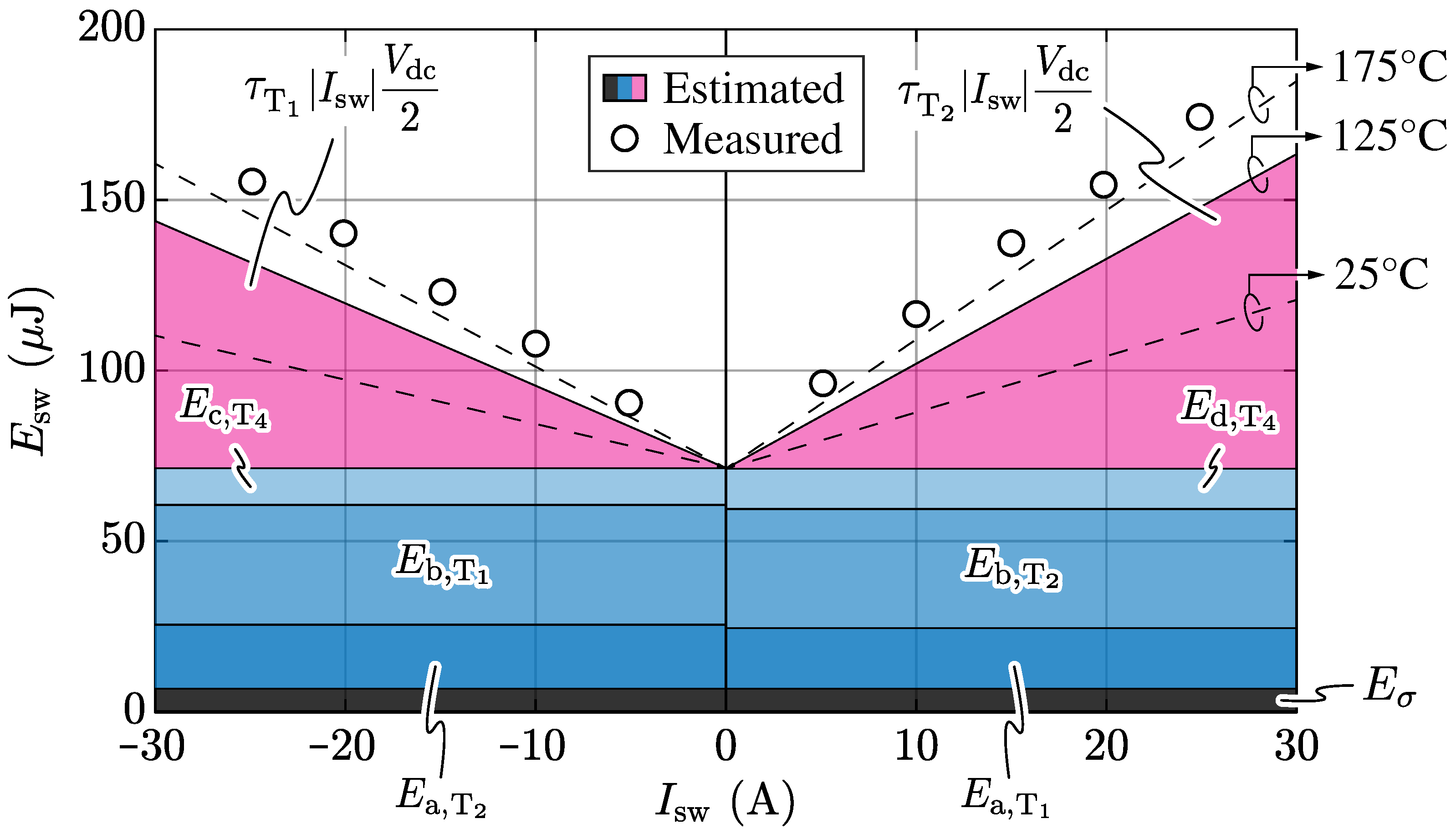
To assess the accuracy of the simplified hard-switching-loss model proposed in
Section 3, loss measurements for positive and negative bridge-leg output currents (
, cf.,
Figure 1) are performed. Due to the temperature dependency of the reverse-recovery time constant
, the bridge-leg duty cycle and switching frequency are adjusted to always achieve an estimated semiconductor junction temperature of around 125 °C (±10 °C). The switching losses are estimated according to the simplified loss model in Equation (
13), i.e.,
As the information of both the 1200 V and 650 V MOSFETs is only provided at Tj = 175 °C; the datasheets belonging to the same semiconductor devices in a different, surface-mount TO-263-7L package are used to extract at Tj = 25 °C, enabling a linear interpolation between the values.
Figure 5 and
Table 1 compare the experimental results and the estimations obtained with the proposed datasheet-based switching-loss model for the 3LTTC, whereby
Figure 5 also provides a breakdown of the the capacitive loss contributions from Equations (
9) or (
10), respectively, and of the reverse-recovery losses. Considering its simplicity, the model predicts the measured hard-switching losses well, achieving a maximum underestimation error of 18% in the considered load current range. The model accuracy reduces with increasing
, as the unaccounted-for
V-
I overlap (caused by the finite
and
values) increasingly affects the overall losses. The deviation between the measured and estimated losses is, in fact, well reflected by the approximate evaluation of the
V-
I overlap losses with Equation (
11), assuming reasonable values of
≈ 100
and
≈ 10
(i.e., according to measurements and datasheet information). As the switching speeds of next-generation WBG power transistors are expected to show an increasing tendency, driven by the trend towards further integration of power electronic converters and, especially, by integrated gate-drive circuits [
20], the accuracy of the proposed loss model is expected to improve further.
5. Conclusions
This paper describes a simplified method to estimate the hard-switching losses in SiC-based three-level T-type (3LTT) bridge-legs. Remarkably, the proposed method is applicable to other three-level topologies as well. Neglecting voltage/current overlap losses and considering only charge-related loss components, the proposed approach requires minimal information from datasheets. It can not only account for the capacitive charge/discharge loss caused by the third semiconductor device that is subject to the voltage transient during hard-switching events, but it is also especially applicable to commutations between semiconductor devices with different blocking voltage and/or current ratings. The proposed loss model is verified experimentally by calorimetrically measuring the switching losses of an 800 V DC-link 3LTT bridge-leg prototype employing 1200 V and 650 V SiC MOSFETs. The results show that, with the proposed model, the basic semiconductor information provided in the datasheet are sufficient to predict the switching losses of the 3LTT with reasonable accuracy, resulting in a maximum underestimation error of 18% with respect to calorimetric measurements.
Whereas a certain loss underestimation must be expected due to not considering the overlap losses (whose importance reduces with increasing switching speeds enabled by future integrated gate drivers), it is worth highlighting that the estimation accuracy strongly depends on the quality of the
information provided by the semiconductor device manufacturers in their datasheets. Unfortunately, this information is often unreliable (e.g., possibly including unwanted high-frequency ringing effects [
17]) and/or is only provided for one operating point (i.e., a single combination of
,
,
). Therefore, better
data quality, considering, for instance, the measurement procedure proposed in [
17], and the availability of more data points in datasheets could further improve the accuracy of the proposed straightforward modeling approach for hard-switching losses in 3LTT (and other three-level) bridge-legs.


