1. Introduction
Thermal imaging, also known as thermography, is constructing a heat map of the surrounding. This is done by detecting the heat signature of the different objects using thermal cameras that operate in the infra-red range (9–14
m). Although thermography started as a military application to detect enemy forces, it has recently found its way to many more applications thanks to its numerous advantages. For example, the dependence on heat allows thermography to operate well in a non-lit environment, and consequently, it is suitable for surveillance applications [
1] and wildlife monitoring [
2]. Thermal imaging can be used to monitor the welfare of the elderly as it only captures the human body temperature and, therefore, does not violate their privacy [
3]. Thermography helps to detect early diseases in humans and plants besides early detection of thermal discomfort among farm animals.
Thermography applications, especially monitoring, produce long sequences of thermal images (or video frames). Different frames are expected to have different significance. For example, while some frames might be safely ignored, others might be essential. An intelligent edge device should not only decide the significance of the frame but also adjust its behavior accordingly. As suggested in [
4], edge devices should adjust their compression rate and activity rate according to the image importance, the battery status, and the remaining operation time.
In this paper, an edge device with a thermal camera, a transmitter, and an Intelligent Thermal Image Processing Unit (ITIPU) is proposed. Detailed design of the ITIPU is provided in
Section 3. Generally, the ITIPU consists of an image classifier, encoder, and controller. The classifier is used to determine the importance of the captured image, the encoder compresses the image before transmission, and the controller makes decisions based on the classifier output. These decisions include deciding the compression rate of the image and the frame rate of the thermal camera. The classification and the compression are both designed based on Convolutional Neural Networks (CNN) architectures with different mathematical operations and different layers. It should be noted that despite the dominant accuracy achieved by the state-of-the-art deep neural networks, this comes with a huge price represented in the computational cost [
5]. This huge computational cost can be observed for example in a simple model such as the LeNet-5 model, which requires about 680 ×
arithmetic operations (addition or multiplication) per classification (op/cl) to carry out a simple MNIST handwritten digits classification, whereas the VGG16 requires about 31G op/cl handling the 1000-class ImageNet task [
5]. As the aim of this work is to design and implement a general-purpose ITIPU, FPGA is an excellent candidate to be used to accelerate our Deep Neural Network (DNN) model besides offering capacity for customization. FPGA is also exploited to offer significant reconfigurability and adaptability during run-time which can be used to reconfigure the programmable logic based on specific pre-defined parameters, such as the remaining battery energy level or data transfer speed. In order to deploy a CNN on the FPGA, long design time might be needed which is a challenging problem, and correspondingly, a great effort is then required to deploy a CNN architecture to an FPGA. Xilinx Inc. has addressed this problem by releasing an Intellectual Property core (IP core) called Deep Learning Processing Unit (DPU). The DPU provides an efficient implementation of different CNN architectures on the FPGA by supporting various deep learning operations. The DPU offers flexibility in the implementation of CNNs on the FPGA as well as efficiency in terms of, design time, energy consumption, and latency.
While this work proposes a compression engine besides a set of classifiers that differ in performance and accuracy, these differences should be leveraged to expand both the adaptive and reconfigurable features of the system in order to address the limitations of the IoT applications and enhance the computational processing capacity. Accordingly, the proposed system should demonstrate a set of crucial specifications and features that would overcome those limitations. Such crucial features are considered to be parallel processing on different levels and reconfigurability. While the former should be realized in executing different tasks (i.e., classification, and compression) simultaneously as well as parallelism on the scale of each task, the latter can be reflected on reconfiguring the system based on a specific sensitivity list.
In this work, an ITIPU based on a unified deep-learning design is proposed. The design is implemented by a DPU on the programmable logic of the Xilinx Zynq UltraScale+ MPSoC ZCU104 FPGA Evaluation Kit. The main aim of the design is to achieve a programmable flexible design with a high image processing throughput and minimum energy consumption. The main contributions of this work are:
An adaptive system is proposed to carry out the image classification and compression. The system is reconfigured based on several parameters such as the battery energy level and the data transfer rate.
To best of the authors’ knowledge, this is the first time such an IP is used in an adaptive scheme in order to maintain the system operation in different scenarios. This promotes its feasibility for IoT applications as it results in lengthening the battery life, especially, in applications with a limited energy budget.
Additionally, the proposed system is capable of executing both classification and compression tasks simultaneously, which boosts the overall system performance.
The experimental results of this work provide useful design recommendations and insights to hardware accelerators designers to reduce the CNN accelerators design time with high throughput and low energy consumption.
The rest of this paper is organized as follows:
Section 3 shows the system-level and
Section 4 shows the proposed designs of deep learning-based image classification and compression. DPU design flow is presented in
Section 5, and the implementation is detailed in
Section 6. Finally,
Section 7 concludes the paper.
2. Related Work
Recently, the authors in [
6] evaluated the performance of the DPU, among other architectures, using different vision kernels and neural networks as benchmarks. The outcomes showed that the DPU-Based accelerator on FPGA outperformed both ARM Cortex A57 CPU with 32-bit floating-point precision and Nvidia Jetson TX2 with 16-bit floating-point precision in terms of the throughput of MobileNet-V2. Furthermore, the accuracy loss observed due to the model compression was negligible (less than 1.1%). With regard to object detection applications, Wang et al. [
7] used the DPU to accelerate YOLOv3 [
8] and compare its performance with its counterpart on Nvidia GeForce GTX1080. While the numerical precision was significantly reduced on the DPU compared to the GPU (8-bit fixed precision and 32-bit floating-point, respectively), the DPU demonstrated more than 2× for single-threaded and 6× while leveraging multi-threading higher throughput than the GPU. In terms of energy efficiency, the DPU processed 3.38 FPS/W whereas the GPU only maintained only 0.26 FPS/W. Similarly, Chan et al. [
9] deployed the same system for robots to detect agricultural crops where the DPU also outperformed both CPU and GPU in terms of power efficiency. From the perspective of the software stack, Zhu et al. [
10] addressed the challenge of optimizing the task scheduler by building a task assignment that uses the Vitis AI software stack. This led to significant improvement in terms of performance. One main problem with the aforementioned work is that the systems demonstrated constant energy consumption that did not change according to certain sensitivities (e.g., the battery lifetime). This may present a challenge for IoT applications to adopt these systems. Accordingly, this work addresses this problem by proposing an energy-adaptive system that features a shorter development time, higher flexibility that covers a wide range of CNN architectures. The other observation is that the prior work evaluated the DPU performance using standardized CNN architectures (e.g., VGG16, ResNet-50, etc.). Thus, the proposed work also addresses this observation by proposing novel CNN architectures for classification and compression.
3. System Design
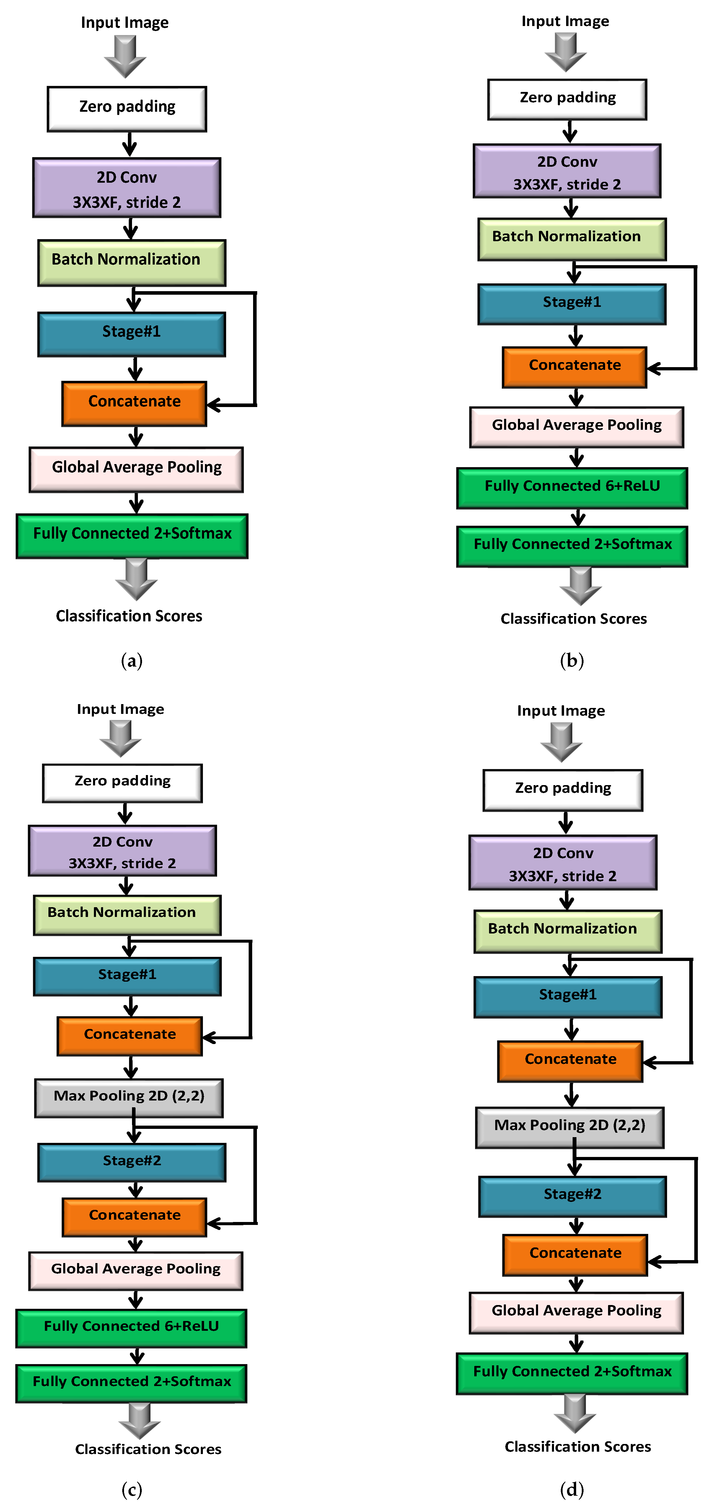
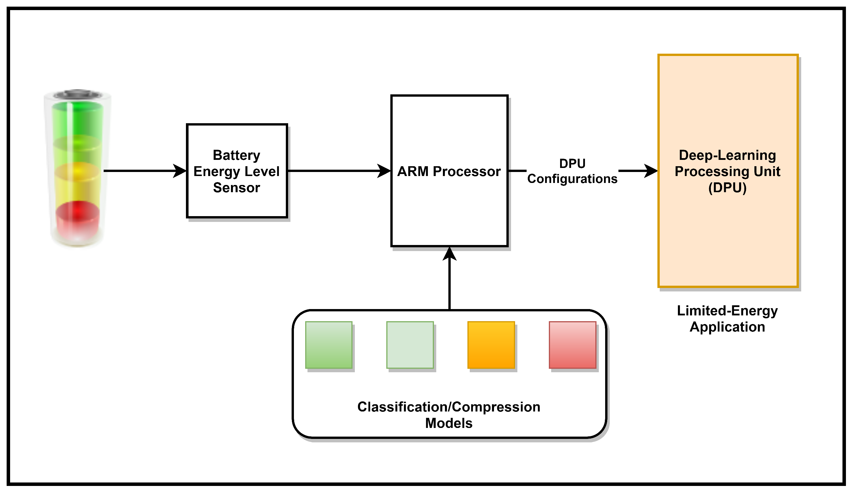
This section describes the system-level design of an intelligent thermal image processing unit (ITIPU). The unit consists of an image classifier, an image compressor, and a controller as shown in
Figure 1. A thermal camera feeds its captured frames to the image classifier, which classifies each frame to a number of predetermined classes. Following that, the frames are compressed by a multi-rate image encoder before being transmitted, over the wireless channel, to the destination. The classification outcome is used as an input to the controller to determine the compression rate of the classified frame. For example, a frame belonging to an unimportant class can be highly compressed (or skipped) in order to save transmission energy. The controller also uses the classification outcome to regulate the frame rate of the thermal camera. For example, it can opt to reduce the frame rate when a series of insignificant or uninteresting frames is received.
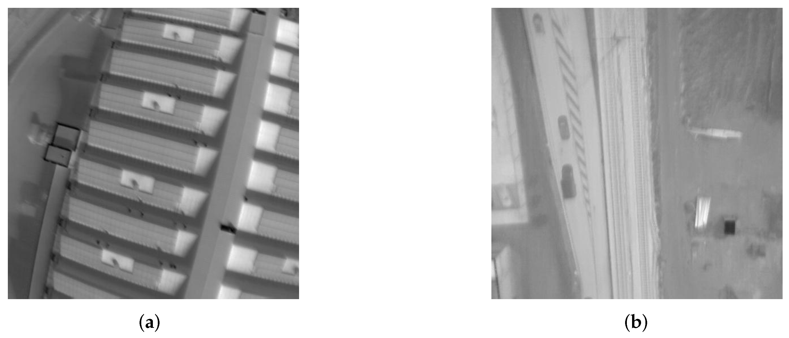
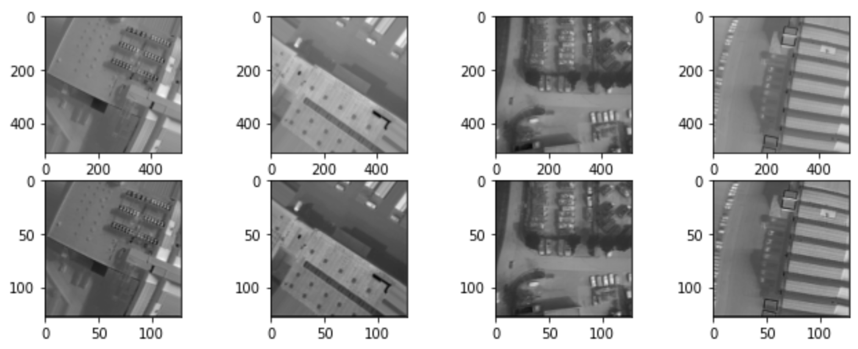
The classification and compression units are designed as CNNs. We use, without loss of generality, the aerial thermal image dataset provided by SenseFly in [
11] to train and test the classification and compression units. The dataset is a series of thermal images captured by a drone that monitors solar panels installation. For classification purposes, the images are grouped into two classes: images with solar panels, and images without solar panels. Sample images of the two classes are shown in
Figure 2. The images are greyscale of size 512 × 512. The following section provides the detailed design of the classification and compression units.
5. DPU Design Flow
5.1. DNN Acceleration
In terms of processing infrastructure, general-purpose processors, such as CPUs and GPUs, have been dominant for years now being deployed for DNN inference, especially the uncompressed DNN models in which the arithmetic operations are represented in floating-point matrix multiplications. However, thanks to the DNN approximation, this has opened the horizons to exploit custom hardware platforms such as Field Programmable Gate Arrays (FPGAs) and Application Specific Integrated Circuits (ASICs) to leverage the usage of fixed-point quantization, which results in faster inference with accuracy reduction less than 1% [
20,
21].
Since the need for faster and real-time inference is becoming more demanding, many hardware companies lean towards the custom hardware approach [
22]. Concerning ASIC, Google’s Tensor Processing Unit (TPU) [
23] represents a good example of a DNN accelerator implemented on ASIC as well as Intel Nervana [
24]. On the other hand, the FPGA-based accelerators are found in Microsoft Brainwave [
25] and Xilinx DPU [
26].
Generally, the acceleration development flow takes one of two approaches to design and implement the accelerator; the first is to design the accelerator in Register-Transfer Level (RTL) using one of the famous Hardware Description Languages (HDL) such as VHDL or Verilog, or to describe the accelerator top-level design in C/C++ then high-level synthesize the code into synthesizable HDL.
Table 3 summarizes the differences between these two approaches in addition to highlighting the privileges of using the DPU as an alternative approach to reduce the accelerator design and development cycle.
The DPU is an IP provided by Xilinx to accelerate DNN models, which provides a high level of parallelism, and energy efficiency that makes it an efficient alternative for IoT devices. Practically, the DPU is a programmable acceleration engine that is not dedicated to a specific CNN model or architecture. This has been achieved by a specialized instruction set that drives the DPU operations, which makes the DPU more generic to work efficiently for many CNN models. The developer is then required to convert the targeted CNN model from the famous DNN frameworks format, such as Tensorflow and Cafe, into the compatible one supported by the DPU engine. This conversion is carried out using a unified software stack called Vitis AI Framework provided by Xilinx. This AI framework is responsible for quantizing and pruning the model, compiling the model into the equivalent instructions that are supported by the DPU, and making performance profiling.
Figure 7 depicts the internal architecture of the DPU, which fundamentally consists of a scheduler module, Processing Engines (PEs), instruction unit block, and global memory pool module. The Application Processing Unit (APU) is the ARM processor, on which the application is running, serves interrupts and data transfer from and to the DPU. The instruction unit handles reading and executing the instructions associated with the different operations of the accelerated CNN. The Fetcher’s main role is to fetch the DPU instructions associated with the model from the memory. Following that, the decoder is responsible for decoding the instructions to drive the PEs. The dispatcher is responsible for managing the data/instructions transfer among the PEs and the memory. The Global Memory Pool acts as a buffer for the input and output data as well as intermediate output from the DPU, which results in high throughput.
In this work, the unified DPU hardware accelerator is used to accelerate all the models proposed without making any modification to the original system setup. The accelerator is configured based on the battery energy level which makes the entire system energy adaptive, as shown in
Figure 8.
5.2. Model Quantization and Compilation
Quantization is the process of representing the data in a smaller number of bits in a scheme that minimizes the error between the original and quantized data. This, accordingly, results in reducing the energy and storage cost area. Therefore, the memory access gets optimized since it dominates the energy consumption [
5]. In this work, the quantization and channel pruning techniques are leveraged to address these issues while achieving high performance and high energy efficiency with little degradation in accuracy.
Within the Vitis AI stack, a specialized quantizer is used to convert the numerical representation of the model weights from 32-bit floating point to 8-bit fixed point precision. Furthermore, the Vitis AI quantizer prunes the network from the ineffective connections, which also enhances the overall accelerator performance.
Besides, the framework also entails a core component, which is the pruner. The pruner is responsible for lowering the number of model weights without resulting in significant precision loss. This happens through an iterative process that takes advantage of the redundant and near-zero parameters, which aims at reducing the number of computations in the model. However, this can cause accuracy loss, which can be overcome by the next stage which is the fine-tuning [
29].
Vitis AI comes with a domain-specific compiler that maps the quantized model into the associated supported sequence of instructions that drive the DPU. This happens by recognizing each layer and convert it into equivalent instructions. By the end of such process, the main goal is to generate the kernels that shall be deployed on the FPGA and then used by some provided API functions to drive the accelerators.
In this work, the Vitis AI compiler is used to compile the classifiers and the compression encoder after quantizing them into 8-bit fixed-point precision. By nature, the compiler supports a range of different CNN layers that can be accelerated by the DPU. However, there are some layers that force the developer to implement them in software so that they will eventually get executed on the CPU which is denoted by Hardware-Software Co-Design. For example, the softmax activation function and the Global Average Pooling Layer are not supported by the DPU, and correspondingly, they have been implemented on the software side.
At the end of the process, the DPU kernels that contain the parameters of the separated regions are generated. In run-time, these kernels shall be loaded into the DPU ahead of propagating the input image over the model. In order to perform this task, Vitis AI provides a uniform coded API that handles the execution of the model on the heterogeneous platform of the CPU and the DPU.
5.3. Vitis AI API
The main objective of the Vitis API functions is to configure the DPU for the CNN model desired to be accelerated. This includes reading the DPU instruction sequence of the model and loading weights in the DPU. Besides, the API functions are used to handle the data exchange between the CPU and the DPU, which allows the data to be pre-processed before being fed to the DPU or post-processed after carrying out the inference, which is accelerated by the DPU.
The Vitis API functions are programmed to load the different classifiers proposed in this work as well as the compression encoders based on several parameters, such as battery energy level, and ata transmission rate. The API propagates the images through the classifier on the DPU for accelerated inference, then takes the output data, which is then used to configure the DPU again with the compression encoder weights and instructions for accelerated compression. Finally, the API takes the compressed image out from the DPU, store it in the off-chip memory, then send it to the specified destination.
5.4. FPGA Implementation of DPU
The DPU hardware accelerator has been implemented on the targeted Xilinx Zynq UltraScale+ MPSoC ZCU104 FPGA Evaluation Kit. Resource utilization and power consumption are considered as the main hardware performance metrics. The DPU design parameters and configurations are elaborated in
Table 4.
As demonstrated in
Figure 7, the DPU is connected to the ARM processor on the FPGA chip to manage task scheduling and offloading weights and data to the DPU. The DPU is connected to the ARM core through an AXI Bus that carries data and weights to the DPU. In addition, Mixed-Mode Clock Manager (MMCM) block is used to generate required frequencies.
Table 5 demonstrates the resources utilization of the DPU on the ZCU 104. The MMCM block consumes less than 1% of the total DPU resources.
Table 6 shows the power consumption of the DPU at 300 MHz. The DPU power consumption and resource utilization are optimized by leveraging special UltraRAM slices [
30]. The UltraRAM is a novel memory solution by Xilinx, which introduces higher memory speed with low energy consumption and resource utilization. The DPU operates with 4 MB memory attached to it coming from both URAM blocks as well as BRAM blocks. This amount of memory is enough for this application and for any future scaling of the system. The floorplan of the DPU is illustrated in
Figure 9.
6. System Setup and Experimental Results
6.1. System Setup
In these experimental results, Xilinx Zynq UltraScale+ MPSoC ZCU104 Evaluation Kit is used.
Figure 10 shows the DPU hardware accelerator coupled with the ARM processor. On the top of the system, the five classifier models and encoder model reside and are managed by a custom API that uses Vitis AI library functions to manage the communications between the APU (The ARM Processor Unit) and the DPU accelerator. The Vitis AI API library communicates with the DPU driver to handle the data movement between both sides of the system, which are all controlled by the Petalinux OS that runs on top of the ARM processor.
The thermal camera sends a number of frames to the APU, which controls the entire system. The frames are then propagated one by one through the classifier in order to determine its class. The output of the inference process is then sent to the APU in order to configure the DPU to accelerate the encoding with the required compression parameters, based on the battery energy level and the transfer rate. Following that, the compressed frames are sent to the specified destination.
At the system level, the data are initially stored in the off-chip DDR-RAM, which is controlled by the DDR-Controller through the AXI-Bus. The system data is initially loaded in the off-chip memory before being moved to the on-chip DPU buffers as a part of configuring the DPU for acceleration. Once the DPU finishes a process, the data is taken from the output on-chip buffers back to memory for any desired post-processing. The data include the model input image, with a size of is 512 × 512, the model weights and biases, and model associated instructions.
On start-up, the DPU fetches the model associated instructions from the off-chip memory, which are then used to control the PEs inside the Hybrid Computing Array shown in
Figure 7. The data is then loaded in the DPU to accelerate the inference (in case of classification) or the compression (in case of accelerating the encoder). To reduce the overall memory bandwidth, the data remain used as much as possible, which enhances the overall performance of the system in terms of latency as well as energy consumption.
Furthermore, the API takes an adaptive approach, based on a set of decision parameters, that picks which classifiers and which encoder compression rate should be used to configure the DPU.
6.2. Experimental Results and Discussions
As the main objective of this flow is to accelerate the inference process while maintaining the lowest accuracy loss, the performance of the proposed system is characterized with respect to certain trade-offs. The performance results are shown in
Table 7 and
Table 8 for the classifiers and the compression engine, respectively, on both CPU and DPU. The performance (i.e., accuracy, speed, and energy) of each model has been evaluated on Intel Core i7-4790 that operates at 3.6 GHz with 16 GB RAM coupled. In this context, the Intel processor is referred to as the CPU platform.
First, the post-quantization accuracy for each model was evaluated using the evaluation model generated by the Vitis AI quantizer using a test set that has 90 test cases. On the other hand, the encoder accuracy is evaluated by estimating the Mean-Squared Error (MSE) between the compressed images before and after quantization based on the evaluation model. In such scenario, the MSE between the original and post-quantization encoder models is
. Additionally,
Figure 11 highlights the differences between the compressed images generated by the original and quantized encoders.
Furthermore, the system throughput is evaluated by the overall inference time on both CPU (Intel Processor) and the FPGA to show the hardware acceleration benefits. The Intel CPU power consumption is estimated to be 84 W [
31]. As demonstrated in
Table 6, the total power consumption of the DPU is measured and equals 11.65 W.
6.2.1. Classifiers
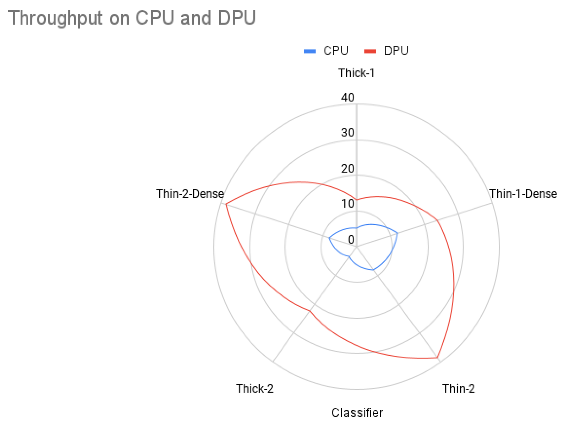
Several trade-offs should be considered in the hardware accelerator design in the proposed system. Firstly, the accuracy loss that results from quantization should be evaluated for each model. In this context, the Thick-1 model has achieved the least accuracy loss of all models, which is nearly 1.45%. On the other hand, the Thin-1-Dense model has achieved the least post-quantization accuracy and accuracy loss which are about 68% and 15.3%, respectively. Moreover, the Thick-2 model has achieved the highest accuracy among all models before and after quantization. The speed increase of the classifiers is ranged from 2× to about 6.4× compared to the CPU (Intel Processor). The former belongs to Thin-1-Dense, while the latter is associated with the Thick-2 model.
Figure 12 reflects the gap between the throughput on the DPU compared to the CPU. In
Figure 13, the number of parameters and the speed increase achieved by the accelerator is plotted. It can be observed that a direct proportion can describe the effect of the number of model parameters on the DPU to accelerate the model inference.
In terms of energy consumption, the DPU achieves a significant reduction in the energy consumed during inference time, which saves at least 93% of its counterpart on the CPU, whereas the maximum energy saving achieved has been 97.8%. As a result, this makes all the models suitable for IoT applications. Based on the battery energy level, one model is configured to the DPU trading-off accuracy to lengthen the battery life [
32]. The gap between the energy consumption on the CPU and the DPU can be realized from
Figure 14.
6.2.2. Compression Encoder
The CNN-based encoder achieves the highest throughput and lowest energy consumption per image compression process, compared to the classifiers. The MSE between the original and the quantized models is
, which is considered insignificant. Hereby, the compressed images should be capable of inheriting the main features of the original images while being significantly compressed. This can be observed by the encoder output images in
Figure 11.
6.3. System Limitations
Despite the fact that the proposed system handles a variety of CNN layers in an energy-adaptive manner, the system still tackles some limitations. Firstly, the current system does not fully leverage multi-core DPU implementation to accelerate one stage of the system on one core and the other stage on the other core. Furthermore, the CNN compiler associated with the DPU (i.e., Vitis AI compiler) does not support some operations like Global Average Pooling and Softmax, hence, these operations have to be handled by the CPU. In such case, the data is moved from the DPU memory to the CPU memory so that the CPU executes these operations then send it back again to the DPU memory to resume the acceleration flow. Hereby, this results in an additional overhead on the system.
7. Conclusions
In this paper, the implementation of an intelligent thermal imaging classification and compression is discussed. The system is adaptive to a set of factors, such as energy budget. Image classification is carried out using different CNN architectures with an average accuracy drop of 4.22% and an average speed increase of 4.11× after deployment on the DPU. A compression model is proposed which compresses the image from 512 × 512 into 128 × 128 pixels using an auto-encoder architecture. After training the auto-encoder, the encoder part, which is used to compress the image, is deployed to the DPU with a speed increase of 5.56×. The compression model can be integrated with another classification model for more optimization in computations and memory usage. The system performs faster than commercial CPUs, which led to a more energy-efficient behavior per frame. Furthermore, in terms of speed increase, it was found that the number of the parameters of the proposed models depicted had a significant impact on the acceleration speed increase rate.In the future, the system can be extended to support manual process assignment to each of the DPU cores so that a higher level of parallelism can be leveraged. Additionally, in order to achieve better optimization, it is important to investigate the software stack of the Vitis-AI to enhance the quantizer and the compiler for more efficient task scheduling.


 ,
, 


