Article

Temperature-Sensitivity of Two Microwave HEMT Devices: AlGaAs/GaAs vs. AlGaN/GaN Heterostructures

by
Mohammad Abdul Alim
1,
Abu Zahed Chowdhury
1,
Shariful Islam
1,
Christophe Gaquiere
2 and
Giovanni Crupi
3,*
1
Department of Electrical and Electronic Engineering, University of Chittagong, Chittagong 4331, Bangladesh
2
Institute of Electronic, Microelectronic and Nanotechnology (IEMN), The University of Lille, F-59000 Lille, France
3
Department of Biomedical and Dental Sciences and Morphofunctional Imaging, University of Messina, 98125 Messina, Italy
*
Author to whom correspondence should be addressed.
Electronics 2021, 10(9), 1115; https://doi.org/10.3390/electronics10091115
Submission received: 22 March 2021 / Revised: 3 May 2021 / Accepted: 4 May 2021 / Published: 9 May 2021
(This article belongs to the Special Issue Microwave Devices Design and Application)

Abstract

:
The goal of this paper is to provide a comparative analysis of the thermal impact on the microwave performance of high electron-mobility transistors (HEMTs) based on GaAs and GaN technologies. To accomplish this challenging goal, the relative sensitivity of the microwave performance to changes in the ambient temperature is determined by using scattering parameter measurements and the corresponding equivalent-circuit models. The studied devices are two HEMTs with the same gate width of 200 µm but fabricated using different semiconductor materials: GaAs and GaN technologies. The investigation is performed under both cooled and heated conditions, by varying the temperature from −40 °C to 150 °C. Although the impact of the temperature strongly depends on the selected operating condition, the bias point is chosen in order to enable, as much as possible, a fair comparison between the two different technologies. As will be shown, quite similar trends are observed for the two different technologies, but the impact of the temperature is more pronounced in the GaN device.

1. Introduction

High electron-mobility transistors (HEMTs, also known as a heterostructure or heterojunction FETs) based on AlGaAs/GaAs and AlGaN/GaN heterostructures have greatly evolved since their inception in the early 1980s [1] and early 1990s [2], respectively. The most evident difference between the GaAs and GaN technologies is that the former is more mature, whereas the latter is more suited for high-power applications, owing to its wide bandgap nature. Over the years, many studies have focused on the high-frequency characterization and modeling of the temperature-dependent behavior of both GaAs [3,4,5,6,7,8,9,10,11,12] and GaN [13,14,15,16,17,18,19,20,21,22,23,24,25,26,27] HEMTs. This is because the operating temperature can remarkably affect the device performance, reliability, and lifetime, which are key features in practical applications, especially those in harsh environmental conditions [28]. With the aim of contributing to the assessment of the impact of the temperature on GaAs and GaN technologies, this article presents a comparative investigation of the temperature-dependent high-frequency behavior of two HEMTs based on AlGaAs/GaAs and AlGaN/GaN heterojunctions. To enable this comparative investigation, a sensitivity-based analysis is developed. The assessment of the sensitivity of the two HEMTs to changes in the ambient temperature (Ta) has been accomplished by using equivalent circuit models extracted from scattering (S-) parameters. The ambient temperature has been swept over a wide range of values, going from −40 °C to 150 °C. The bias point has been selected in order to allow, as much as possible, a fair comparison between the two different transistor technologies. The GaAs and GaN HEMTs have the same gate width of 200 μm but differ in the gate lengths, which are 0.25 μm and 0.5 μm, respectively. For the first time, the challenging task of comparing the temperature-dependent performance of the two different semiconductor technologies is accomplished by reporting an extensive and systematic sensitivity-based analysis, which is carried out by using the drain current (Ids), the equivalent-circuit parameters (ECPs), and the major RF figures of merit. The degradations of the device performance at a higher Ta are found to be more pronounced for the GaN technology, which can be attributed to the higher dissipated power (Pdiss). It is worth noting that the two tested technologies are inherently different and that this then clearly impacts on the achieved results. Given the widely different characteristics of the two tested technologies, it is really not feasible to distinguish each contribution arising from the different operating conditions (e.g., dissipated power) and peculiar device physics (e.g., thickness and thermal conductivity of the substrate). Hence, the reported comparative analysis has not aimed at distinguishing each contribution but at assessing the overall impact of the ambient temperature on the DC and microwave characteristics of the two tested technologies. Nevertheless, for the sake of completeness, it should be underlined that the channel temperature is higher than the ambient temperature because of the heat generated by the self-heating effects, which are strongly dependent not only on the dissipated power level but also on the thickness and thermal conductivity of the materials [13,29,30,31,32,33,34,35,36]. Furthermore, it is worth mentioning that the extraction of the equivalent-circuit elements may be inevitable affected by the uncertainty inherent in measurements and that, in addition, the model topology itself is an approximation of the device physics [37,38,39,40,41,42,43], which in turn may impact on the achieved temperature-dependent findings.
The remainder of this article is organized as follows: Section 2 is focused on the description of the tested device and experiments, Section 3 is devoted to the sensitivity-based analysis and the discussion of the findings, and the last section summarizes the main conclusions of this study.

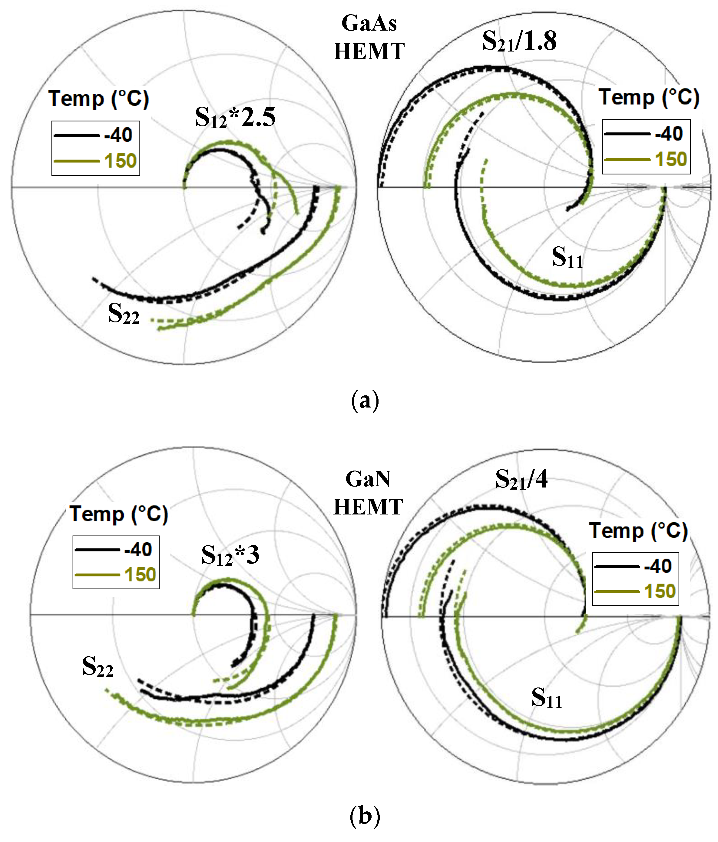
2. Devices and Experiments

The two studied devices are an AlGaAs/GaAs HEMT grown by molecular beam epitaxy (MBE) on a semi-insulating undoped GaAs substrate and an AlGaN/GaN HEMT grown by metal-organic chemical vapor deposition (MOCVD) on a SiC substrate. Figure 1 shows the schematic cross-sectional views and photos of the two tested HEMTs. The interdigitated layout of both devices is based on the connection in parallel of two fingers, each being 100-μm long, yielding to a total gate width of 200 μm. The gate lengths of the GaAs and GaN devices are 0.25 μm and 0.5 μm, respectively. The source-to-gate distance (LSG) and the gate-to-drain distance (LGD) are 0.5 μm and 2.0 μm for the GaAs device, while their values are equal to 1 μm and 2.75 μm for the GaN device.
The microwave experiment consists of S-parameters measured from 45 MHz to 50 GHz at nine different ambient temperatures: −40 °C, −25 °C, 0 °C, 25 °C, 50 °C, 75 °C, 100 °C, 125 °C, and 150 °C. The S-parameters were measured with a vector network analyzer (VNA HP8510C) in conjunction with a DC source (HP4142B) for biasing, a temperature control unit (Temptronic TP03200, Temptronic Corporation, Mansfield, MA, USA) for setting the ambient temperature, and a PC with a specialized software (IC-CAP) for controlling the full measurement procedure through the GPIB interface. The off-wafer calibration was performed using line-reflect-reflect-match (LRRM) standards on the alumina calibration substrate from Cascade Microtech and a commercial calibration software (WinCal). The comparative analysis is performed using S-parameters at the following two bias points in the saturation region: Vds = 3 V and Vgs = −0.1 V for the GaAs HEMT and Vds = 9 V and Vgs = −4 V for the GaN HEMT. This choice has been made based on the analysis of the DC output characteristics of the two transistors at different Ta (see Figure 2 and Figure 3), in order to enable, as much as possible, a fair comparison between the two different technologies. For the GaAs HEMT, two temperature-dependent effects contribute in opposite ways to the resultant behavior of Ids with an increasing temperature: the degradation of the carrier transport properties and the threshold voltage (Vth) shift towards more negative values. Therefore, Vgs is selected at −0.1 V, in order to minimize the contribution of the Vth shift that plays a more dominant role at lower Vgs. Vds is selected at 3 V, in order to avoid the pronounced positive slope of Ids at high Vds. For the GaN HEMT, the temperature-dependent behavior of Ids is mostly due to the degradation of the carrier transport properties and/or to a reduction in the carrier concentration in the two-dimensional electron gas (2DEG). Therefore, Vds and Vgs are, respectively, selected at 9 V and −4 V, in order to avoid the pronounced negative slope of Ids (Vds) at a high Pdiss.
At the selected bias voltages (see Figure 4), the dimensionless relative sensitivity of Ids with respect to Ta is calculated by normalizing the relative change in Ids to the relative change in Ta:
R S I d s = Δ I d s I d s 0 T a 0 Δ T a = ( I d s I d s 0 ) I d s 0 T a 0 ( T a T a 0 )
where Ids0 is the value of Ids at the reference temperature (Ta0) of 25 °C. As can be observed in Figure 4, RSIds is negative for both devices, as a consequence of the fact that an increase in Ta leads to a decrease in Ids, and is of greater magnitude for the GaN technology, as a consequence of the much higher Pdiss leading to a higher channel temperature (i.e., Tch = Ta + RthPdiss where Rth is the thermal resistance).
For the sake of completeness, we report the impact of the ambient temperature on the Ids-Vgs curves and the corresponding transconductance at Vds = 3 V for the GaAs device and at Vds = 9 V for the GaN device (see Figure 5). By increasing the temperature, the drain current and the transconductance are remarkably reduced for the GaN device, whereas operating bias points at which their values are temperature insensitive (the so-called current and transconductance zero temperature coefficient (CZTC and GZTC) points) can be observed for the GaAs device, owing to the counterbalancing of temperature-dependent effects contributing in opposite ways [12].
Figure 6 shows the impact of Ta on the measured S-parameters at the selected bias points. By increasing Ta, the low-frequency S21 is reduced, due to the degradation of the carrier transport properties. Both devices are affected by the kink effect in S22 [44,45,46,47,48,49], which is more marked at a lower Ta because of the higher gm. As a matter of fact, it has been demonstrated that the kink effect is mainly due to high values of gm.

3. Sensitivity-Based Analysis

The S-parameters have been modelled using the equivalent-circuit model in Figure 7. The ECPs have been obtained by using a standard “cold” pinch-off approach [50]. As illustrated in Figure 8, a good agreement between the measured and simulated S-parameter has been achieved for the two tested devices.
Table 1 reports the values of the drain current, the ECPs, the intrinsic input and feedback time constants (i.e., τgs = RgsCgs and τgd = RgdCgd), the unity current gain cut-off frequency (ft), and the maximum frequency of oscillation (fmax). The three intrinsic time constants (τm, τgs, and τgd) model the intrinsic non-quasi-static (NQS) effects, which arise from the inertia of the intrinsic device in responding to rapid signal changes [51]. The values of ft and fmax are, respectively, determined from the measured short-circuit current gain (h21) and maximum stable/available gain (MSG/MAG). Although the GaAs HEMT has a shorter gate length that should result in a higher operation frequency, the GaN HEMT has smaller time constants (except for τgd) and higher ft and fmax, which are desired in order to enable device applications at high frequencies. This is can be linked to the fact that the conventional scaling rules cannot be directly applied to make a straightforward comparison between devices that are based on different semiconductor materials, technologies, and layouts. As a matter of fact, this could be foreseen from the values of Ids, which are larger for the GaN HEMT, even if the GaAs HEMT has a shorter gate length that should result in a higher Ids. The same observation can be made for the intrinsic gm.
Likewise, in the case of Ids, the relative sensitivities of the other parameters in Table 1 are estimated by using Equation (1) and are then illustrated in Figure 9, Figure 10 and Figure 11. Relative sensitivities of the extrinsic capacitances and inductances of close to zero were achieved (see Figure 9a–e), owing to their weak temperature dependence. On the other hand, the relative sensitivities of the extrinsic and intrinsic resistances are positive (see Figure 9f–h and Figure 10d–f), due to the increase of the resistive contributions with an increasing Ta. Contrary to the resistances, the transconductance shows a relative sensitivity that is negative (see Figure 11a), enlightening its degradation with an increasing Ta. The relative sensitivities of the intrinsic capacitances can be positive or negative (see Figure 10a–c), depending on the considered device and capacitance. The relative sensitivities of the intrinsic time constants are positive (see Figure 11b–d), reflecting their increase at a higher Ta and thus a shift of the onset of the NQS effects at lower frequencies. On the other hand, the relative sensitivities of the frequencies ft and fmax are negative (see Figure 11e,f), reflecting their decrease at a higher Ta and thus a reduction of the device operation frequencies. The analysis of the relative sensitivities of the crucial parameters such as gm, ft, and fmax shows that larger negative values are observed for the GaN device compared to the GaAs counterpart (see Figure 11a,e,f), in line with what was seen for Ids (see Figure 4).

4. Conclusions

For the first time, an extensive and systematic comparative analysis of the GaAs and GaN HEMT technologies has been performed by investigating the impact of the temperature variations on the device performance in terms of the relative sensitivities of Ids, ECPs, and major RF figures of merit over a broad temperature range, spanning from −40 °C to 150 °C. By increasing Ta, performance degradations are observed for both devices but they are more pronounced for the GaN technology. This can be attributed to the higher Pdiss leading to a stronger degradation of the electron transport properties.
It is worth pointing out that establishing a fair comparison between the temperature-dependent performance of such inherently widely different semiconductor technologies is a very challenging task, since it is hard to define “homogeneous” operating conditions for devices exhibiting highly “heterogeneous” performances (e.g., the current density has to be referred to the tested technology) and to distinguish each contribution arising from the different peculiar features (e.g., different thermal conductivities of the substrates). In light of that, the selection of relatively balanced bias conditions has been based on the analysis of the specific DC output characteristics and then used as the benchmark for assessing the overall impact of Ta on the microwave characteristics of the two devices. The relative sensitivity has been chosen as an assessment indicator as this parameter allows one to evaluate quantitatively, systematically, and straightforwardly the impact of Ta on the microwave characteristics. Although the achieved findings are not of general validity as they can depend on the combined effects of ECPs whose values can change with the specific device, the investigation methodology is technology-independent and straightforwardly applicable to other FETs in order to target a quantitative and systematic comparison.

Author Contributions

Conceptualization, M.A.A. and G.C.; methodology, M.A.A. and G.C.; validation, M.A.A., A.Z.C. and S.I.; investigation, M.A.A., A.Z.C. and S.I.; writing—original draft preparation, M.A.A., A.Z.C., S.I. and C.G.; writing—review and editing, C.G. and G.C.; supervision, C.G. and G.C. All authors have read and agreed to the published version of the manuscript.

Funding

This research received no external funding.

Conflicts of Interest

The authors declare no conflict of interest. The funders had no role in the design of the study; in the collection, analyses, or interpretation of data; in the writing of the manuscript, or in the decision to publish the results.

References

  1. Mimura, T.; Hiyamizu, S.; Fujii, T.; Nanbu, K. A new field-effect transistor with selectively doped GaAs/n-AlxGa1-x as heterojunctions. Jpn. J. Appl. Phys. 1980, 19, L225–L227. [Google Scholar] [CrossRef]
  2. Khan, M.A.; Bhattarai, A.; Kuznia, J.N.; Olson, D.T. High electron mobility transistor based on a GaN-AlxGa1-xN heterojunction. Appl. Phys. Lett. 1993, 63, 1214–1215. [Google Scholar] [CrossRef]
  3. Belache, A.; Vanoverschelde, A.; Salmer, G.; Wolny, M. Experimental analysis of HEMT behavior under low-temperature conditions. IEEE Trans. Electron Dev. 1991, 38, 3–13. [Google Scholar] [CrossRef]
  4. Anholt, R.E.; Swirhun, S.E. Experimental investigation of the temperature dependence of GaAs FET equivalent circuits. IEEE Trans. Electron Dev. 1992, 39, 2029–2036. [Google Scholar] [CrossRef]
  5. Marinkovic, Z.; Markovic, V. Temperature-dependent models of low-noise microwave transistors based on neural networks. Int. J. RF Microw. Comput. Aided Eng. 2005, 15, 567–577. [Google Scholar] [CrossRef]
  6. Caddemi, A.; Crupi, G.; Donato, N. On the soft breakdown phenomenon in AlGaAs/InGaAs HEMT: An experimental study down to cryogenic temperature. Solid State Electron. 2005, 49, 928–934. [Google Scholar] [CrossRef]
  7. Caddemi, A.; Crupi, G.; Donato, N. Temperature effects on DC and small signal RF performance of AlGaAs/GaAs HEMTs. Microelectron. Reliab. 2006, 46, 169–173. [Google Scholar] [CrossRef]
  8. Huang, J.C.; Hsu, W.C.; Lee, C.S.; Huang, D.H.; Huang, M.F. Temperature-dependent characteristics of enhancement-/depletion-mode double-doped AlGaAs/InGaAs pHEMTs and their monolithic DCFL integrations. Solid State Electron. 2007, 51, 882–887. [Google Scholar] [CrossRef]
  9. Zhu, Y.; Karalkar, S.; Prasad, K.; Wei, C.; Mason, J.; Bartle, D. Temperature dependent linear HEMT model extracted with multi-temperature optimization. In Proceedings of the Asia Pacific Microwave Conference, Kaohsiung, Taiwan, 4–7 December 2012; pp. 756–759. [Google Scholar] [CrossRef]
  10. Alim, M.A.; Rezazadeh, A.A. Temperature-dependent DC and small-signal analysis of AlGaAs/InGaAs pHEMT for high frequency applications. IEEE Trans. Electron Dev. 2016, 63, 1005–1012. [Google Scholar] [CrossRef]
  11. Alim, M.A.; Rezazadeh, A.A. Device behaviour and zero temperature coefficients analysis for microwave GaAs HEMT. Solid State Electron. 2018, 147, 13–18. [Google Scholar] [CrossRef]
  12. Alim, M.A.; Rezazadeh, A.A.; Crupi, G. Experimental insight into the temperature effects on DC and microwave characteristics for a GaAs pHEMT in multilayer 3-D MMIC technology. Int. J. RF Microw. Comput. Aided Eng. 2020, 30, e22379. [Google Scholar] [CrossRef]
  13. Gryglewski, D.; Wojtasiak, W.; Kamińska, E.; Piotrowska, A. Characterization of self-heating process in GaN-based HEMTs. Electronics 2020, 9, 1305. [Google Scholar] [CrossRef]
  14. Camarchia, V.; Cappelluti, F.; Pirola, M.; Guerrieri, S.D.; Ghione, G. Self-consistent electrothermal modeling of class A, AB, and B power GaN HEMTs under modulated RF excitation. IEEE Trans. Microw. Theory Tech. 2007, 55, 1824–1831. [Google Scholar] [CrossRef]
  15. Darwish, A.M.; Huebschman, B.D.; Viveiros, E.; Hung, H.A. Dependence of GaN HEMT millimeter-wave performance on temperature. IEEE Trans. Microw. Theory Tech. 2009, 57, 3205–3211. [Google Scholar] [CrossRef]
  16. Vitanov, S.; Palankovski, V.; Maroldt, S.; Quay, R. High-temperature modeling of AlGaN/GaN HEMTs. Solid State Electron. 2010, 54, 1105–1112. [Google Scholar] [CrossRef]
  17. Crupi, G.; Avolio, G.; Raffo, A.; Barmuta, P.; Schreurs, D.M.M.-P.; Caddemi, A.; Vannini, G. Investigation on the thermal behavior for microwave GaN HEMTs. Solid State Electron. 2011, 64, 28–33. [Google Scholar] [CrossRef]
  18. Angelotti, A.M.; Gibiino, G.P.; Florian, C.; Santarelli, A. Trapping dynamics in GaN HEMTs for millimeter-wave applications: Measurement-based characterization and technology comparison. Electronics 2021, 10, 137. [Google Scholar] [CrossRef]
  19. Marinković, Z.; Crupi, G.; Caddemi, A.; Avolio, G.; Raffo, A.; Marković, V.; Vannini, G.; Schreurs, D.M.M.-P. Neural approach for temperature dependent modeling of GaN HEMTs. Int. J. Numer. Model. Electron. Netw. Devices Fields 2015, 28, 359–370. [Google Scholar] [CrossRef]
  20. Crupi, G.; Raffo, A.; Avolio, G.; Schreurs, D.M.M.-P.; Vannini, G.; Caddemi, A. Temperature influence on GaN HEMT equivalent circuit. IEEE Microw. Wirel. Comp. Lett. 2016, 26, 813–815. [Google Scholar] [CrossRef]
  21. Jarndal, A.; Ghannouchi, F.M. Improved modeling of GaN HEMTs for predicting thermal and trapping-induced-kink effects. Solid-State Electron. 2016, 123, 19–25. [Google Scholar] [CrossRef]
  22. Alim, M.A.; Rezazadeh, A.A.; Gaquiere, C. Temperature effect on DC and equivalent circuit parameters of 0.15-μm gate length GaN/SiC HEMT for microwave applications. IEEE Trans. Microw. Theory Tech. 2016, 64, 3483–3491. [Google Scholar] [CrossRef]
  23. Rodríguez, R.; González, B.; García, J.; Núñez, A. Electrothermal DC characterization of GaN on Si MOS-HEMTs. Solid-State Electron. 2017, 137, 44–51. [Google Scholar] [CrossRef]
  24. Jarndal, A. Neural network electrothermal modeling approach for microwave active devices. Int. J. RF Microw. Comput. Aided Eng. 2019, 29, e21764. [Google Scholar] [CrossRef]
  25. Crupi, G.; Raffo, A.; Vadalà, V.; Vannini, G.; Caddemi, A. High-periphery GaN HEMT modeling up to 65 GHz and 200 °C. Solid-State Electron. 2019, 152, 11–16. [Google Scholar] [CrossRef]
  26. Chen, Y.; Xu, Y.; Zhou, J.; Kong, Y.; Chen, T.; Zhang, Y.; Yan, B.; Xu, R. Temperature-dependent small signal performance of GaN-on-diamond HEMTs. Int. J. Numer. Model. Electron. Netw. Devices. Field 2020, 33, e2620. [Google Scholar] [CrossRef]
  27. Majumdar, A.; Chatterjee, S.; Chatterjee, S.; Chaudhari, S.S.; Poddar, D.R. An ambient temperature dependent small signal model of GaN HEMT using method of curve fitting. Int. J. RF Microw. Comput. Aided Eng. 2020, 30, e22434. [Google Scholar] [CrossRef]
  28. Giofré, R.; Colantonio, P.; Gonzalez, L.; De Arriba, F.; Cabria, L.; Molina, D.L.; Garrido, E.C.; Vitobello, F. Design realization and tests of a space-borne GaN solid state power amplifier for second generation Galileo navigation system. IEEE Trans. Aerosp. Electron. Syst. 2018, 54, 2383–2396. [Google Scholar] [CrossRef]
  29. Darwish, A.M.; Bayba, A.J.; Hung, H.A. Accurate determination of thermal resistance of FETs. IEEE Trans. Microw. Theory Tech. 2005, 53, 306–313. [Google Scholar] [CrossRef]
  30. Sarua, A.; Ji, H.; Hilton, K.P.; Wallis, D.J.; Uren, M.J.; Martin, T.; Kuball, M. Thermal boundary resistance between GaN and substrate in AlGaN/GaN electronic devices. IEEE Tran. Electron Dev. 2007, 54, 3152–3158. [Google Scholar] [CrossRef]
  31. Kuzmík, J.; Bychikhin, S.; Pogany, D.; Gaquière, C.; Pichonat, E.; Morvan, E. Investigation of the thermal boundary resistance at the III-nitride/substrate interface using optical methods. J. Appl. Phys. 2007, 101, 054508-1–054508-6. [Google Scholar] [CrossRef]
  32. Florian, C.; Santarelli, A.; Cignani, R.; Filicori, F. Characterization of the nonlinear thermal resistance and pulsed thermal dynamic behavior of AlGaN–GaN HEMTs on SiC. IEEE Trans. Microw. Theory Tech. 2013, 61, 1879–1891. [Google Scholar] [CrossRef]
  33. Coutu, R.; Lake, R.; Christiansen, B.; Heller, E.; Bozada, C.; Poling, B.; Via, G.; Theimer, J.; Tetlak, S.; Vetury, R.; et al. Benefits of considering more than temperature acceleration for GaN HEMT life testing. Electronics 2016, 5, 32. [Google Scholar] [CrossRef] [Green Version]
  34. Zheng, Q.; Li, C.; Rai, A.; Leach, J.H.; Broido, D.A.; Cahill, D.G. Thermal conductivity of GaN, 71GaN, and SiC from 150 K to 850 K. Phys. Rev. Mater. 2019, 3, 014601. [Google Scholar] [CrossRef]
  35. Jang, K.-W.; Hwang, I.-T.; Kim, H.-J.; Lee, S.-H.; Lim, J.-W.; Kim, H.-S. Thermal analysis and operational characteristics of an AlGaN/GaN high electron mobility transistor with copper-filled structures: A simulation study. Micromachines 2019, 11, 53. [Google Scholar] [CrossRef] [PubMed] [Green Version]
  36. Mitterhuber, L.; Hammer, R.; Dengg, T.; Spitaler, J. Thermal characterization and modelling of AlGaN-GaN multilayer structures for HEMT applications. Energies 2020, 13, 2363. [Google Scholar] [CrossRef]
  37. Walters, P.; Pollard, R.; Richardson, J.; Gamand, P.; Suchet, P. On-wafer measurement uncertainty for 3-terminal active millimetre-wave devices. In Proceedings of the GaAs IC Symposium Technical Digest 1992, Miami Beach, FL, USA, 4–7 October 1992; pp. 55–58. [Google Scholar]
  38. Lewandowski, A.; Williams, D.F.; Hale, P.D.; Wang, J.C.M.; Dienstfrey, A. Covariance-based vector-network-analyzer uncertainty analysis for time-and frequency-domain measurements. IEEE Trans. Microw. Theory Tech. 2010, 58, 1877–1886. [Google Scholar] [CrossRef]
  39. Garelli, M.; Ferrero, A. A unified theory for S-parameter uncertainty evaluation. IEEE Trans. Microw. Theory Tech. 2012, 60, 3844–3855. [Google Scholar] [CrossRef]
  40. King, F.D.; Winson, P.; Snider, A.D.; Dunleavy, L.; Levinson, D.P. Math methods in transistor modeling: Condition numbers for parameter extraction. IEEE Trans. Microw. Theory Tech. 1998, 46, 1313–1314. [Google Scholar] [CrossRef]
  41. Fager, C.; Linner, L.J.P.; Pedro, J.C. Optimal parameter extraction and uncertainty estimation in intrinsic FET small-signal models. IEEE Trans. Microw. Theory Tech. 2002, 50, 2797–2803. [Google Scholar] [CrossRef]
  42. Luo, D.; Shen, L.; Gao, J. An improved linear modeling technique with sensitivity analysis for GaN HEMT. Int. J. Numer. Model. Electron. Netw. Devices Fields 2017, 30, e2139. [Google Scholar] [CrossRef]
  43. Cao, K.-J.; Zhang, A.; Gao, J. Sensitivity analysis and uncertainty estimation in small-signal modeling for InP HBT (invited paper). Int. J. Numer. Model. Electron. Netw. Devices Fields 2021, 1–11. [Google Scholar] [CrossRef]
  44. Lu, S.-S.; Chen, T.-W.; Chen, H.-C.; Meng, C. The origin of the kink phenomenon of transistor scattering parameter S22. IEEE Trans. Microw. Theory Tech. 2001, 49, 333–340. [Google Scholar] [CrossRef]
  45. Crupi, G.; Raffo, A.; Caddemi, A.; Vannini, G. The kink phenomenon in the transistor S22: A systematic and numerical approach. IEEE Microw. Wirel. Comp. Lett. 2012, 22, 406–408. [Google Scholar] [CrossRef]
  46. Crupi, G.; Raffo, A.; Marinkovic, Z.; Avolio, G.; Caddemi, A.; Markovic, V.; Vannini, G.; Schreurs, D.M.M.-P. An extensive experimental analysis of the kink effects in S22 and h21 for a GaN HEMT. IEEE Trans. Microw. Theory Tech. 2014, 62, 513–520. [Google Scholar] [CrossRef]
  47. Ahsan, S.A.; Ghosh, S.; Khandelwal, S.; Chauhan, Y.S. Modeling of kink-effect in RF behaviour of GaN HEMTs using ASM-HEMT model. In Proceedings of the IEEE International Conference Electron Devices Solid-State Circuits, Hong Kong, China, 3–5 August 2016; pp. 426–429. [Google Scholar] [CrossRef]
  48. Alim, M.A.; Rezazadeh, A.A.; Gaquiere, C.; Crupi, G. Thermal influence on S22 kink behavior of a 0.15-μm gate length AlGaN/GaN/SiC HEMT for microwave applications. Semicond. Sci. Tech. 2019, 34, 1–8. [Google Scholar] [CrossRef]
  49. Crupi, G.; Raffo, A.; Vadalà, V.; Vannini, G.; Caddemi, A. A new study on the temperature and bias dependence of the kink effects in S22 and h21 for the GaN HEMT Technology. Electronics 2018, 7, 353. [Google Scholar] [CrossRef] [Green Version]
  50. Crupi, G.; Caddemi, A.; Schreurs, D.M.M.-P.; Dambrine, G. The large world of FET small-signal equivalent circuits. Int. J. RF Microw. Comput. Aided Eng. 2016, 26, 749–762. [Google Scholar] [CrossRef]
  51. Crupi, G.; Schreurs, D.M.M.-P.; Caddemi, A.; Raffo, A.; Vannini, G. Investigation on the non-quasi-static effect implementation for millimeter-wave FET models. Int. J. RF Microw. Comput. Aided Eng. 2010, 20, 87–93. [Google Scholar] [CrossRef]
Figure 1. Schematic cross-sectional views and photos of the tested high electron-mobility transistors (HEMTs) based on (a,c) AlGaAs/GaAs and (b,d) AlGaN/GaN heterostructures.
Electronics 10 01115 g001
Figure 2. DC output characteristics of the studied GaAs HEMT at different Ta.
Electronics 10 01115 g002
Figure 3. DC output characteristics of the studied GaN HEMT at different Ta.
Electronics 10 01115 g003
Figure 4. (a) The selected bias points for the sensitivity-based analysis are Vds = 3 V and Vgs = −0.1 V for the GaAs HEMT (top plot) and Vds = 9 V and Vgs = −4 V for the GaN HEMT (bottom plot); (b) Behavior of RSIds versus Ta for the studied (red line) GaAs and (blue line) GaN HEMTs.
Electronics 10 01115 g004
Figure 5. DC transcharacteristics and transconductances at different Ta for (a,c) the GaAs HEMT at Vds = 3 V and (b,d) the GaN HEMT at Vds = 9 V.
Electronics 10 01115 g005aElectronics 10 01115 g005b
Figure 6. Measured S-parameters of the studied (a) GaAs and (b) GaN HEMTs at different Ta. The illustrated bias points are: Vds = 3 V and Vgs = −0.1 V for the GaAs HEMT and Vds = 9 V and Vgs = −4 V for the GaN HEMT. The frequency range goes from 45 MHz to 50 GHz. (“*” means product (the multiplication operation)).
Electronics 10 01115 g006
Figure 7. Equivalent-circuit model for the studied GaAs and GaN HEMTs.
Electronics 10 01115 g007
Figure 8. Measured S-parameters of the studied (a) GaAs and (b) GaN HEMTs at different Ta. The illustrated bias points are: Vds = 3 V and Vgs = −0.1 V for the GaAs HEMT and Vds = 9 V and Vgs = −4 V for the GaN HEMT. The frequency range goes from 45 MHz to 50 GHz. (“*” means product (the multiplication operation)).
Electronics 10 01115 g008
Figure 9. Behavior of the relative sensitivities of the extrinsic parameters versus Ta for the two studied devices.
Electronics 10 01115 g009
Figure 10. Behavior of the relative sensitivities of the intrinsic resistances and capacitances versus Ta for the two studied devices. The illustrated bias points are: Vds = 3 V and Vgs = −0.1 V for the GaAs HEMT and Vds = 9 V and Vgs = −4 V for the GaN HEMT.
Electronics 10 01115 g010
Figure 11. Behavior of the relative sensitivities of the intrinsic transconductance, the intrinsic time constants, and the RF figures of merit versus Ta for the two studied devices. The illustrated bias points are: Vds = 3 V and Vgs = −0.1 V for the GaAs HEMT and Vds = 9 V and Vgs = −4 V for the GaN HEMT.
Electronics 10 01115 g011
Table 1. Parameters for GaAs and GaN HEMTs at 25 °C.
ParametersGaAs HEMTGaN HEMT
Ids (mA)14.763.5
Cpg (fF)13.132.0
Cpd (fF)41.650.0
Lg (pH)104.0142.0
Ls (pH)5.411.43
Ld (pH)37.884.0
Rg (Ω)2.32.7
Rs (Ω)4.03.1
Rd (Ω)6.38.2
Cgs (fF)275.0199.9
Cgd (fF)30.426.9
Cds (fF)55.989.2
Rgs (Ω)1.51.2
Rgd (Ω)6.313.0
Rds (Ω)360.0322.4
gm (mS)29.663.0
τm (ps)3.81.8
τgs (ps)2.61.5
τgd (ps)1.22.2
ft (GHz)14.940.0
fmax (GHz)44.897.0
Publisher’s Note: MDPI stays neutral with regard to jurisdictional claims in published maps and institutional affiliations.

