
Energy Efficient Self-Adaptive Dual Mode Logic Address Decoder

 ,
,  ,
,  ,
,  , ,
, ,  , , and
Abstract
:1. Introduction
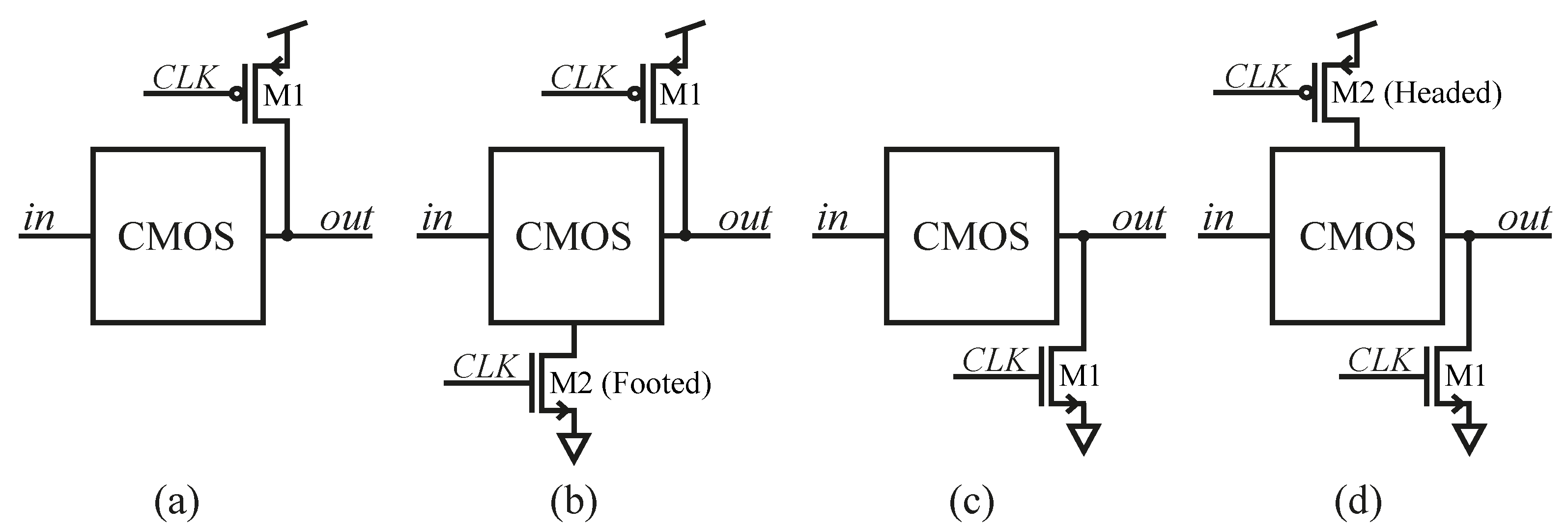
2. Dual Mode Logic Overview
3. Address Decoder Design
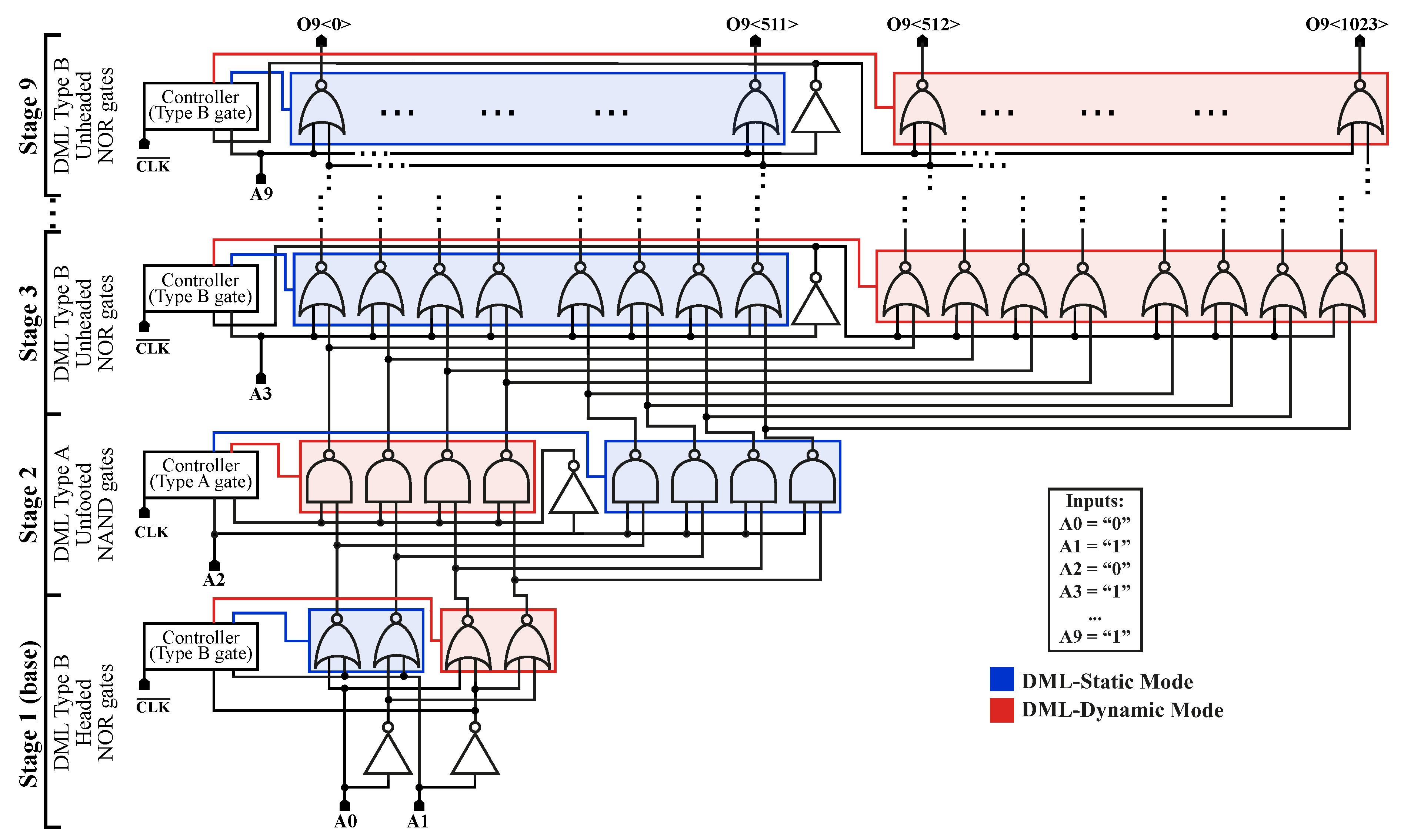
3.1. Address Decoder Architecture
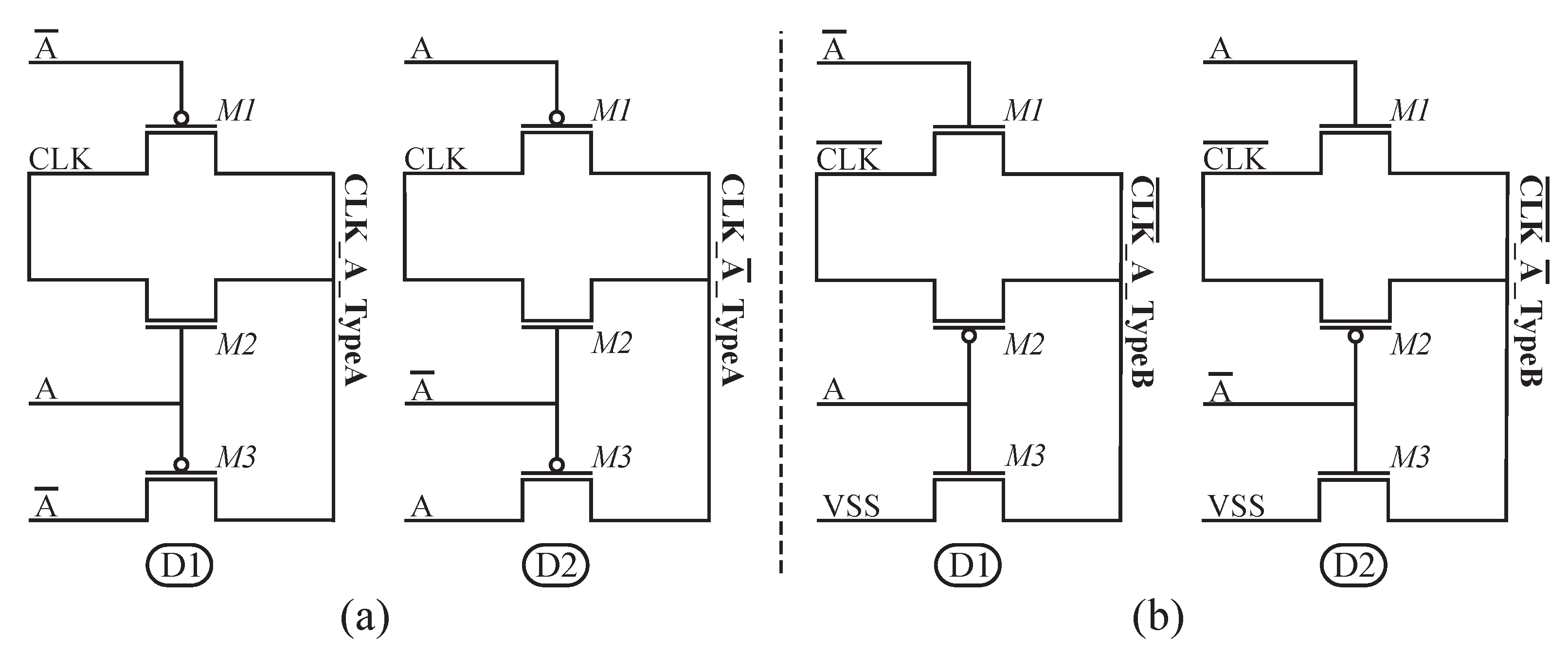
3.2. Decision Logic
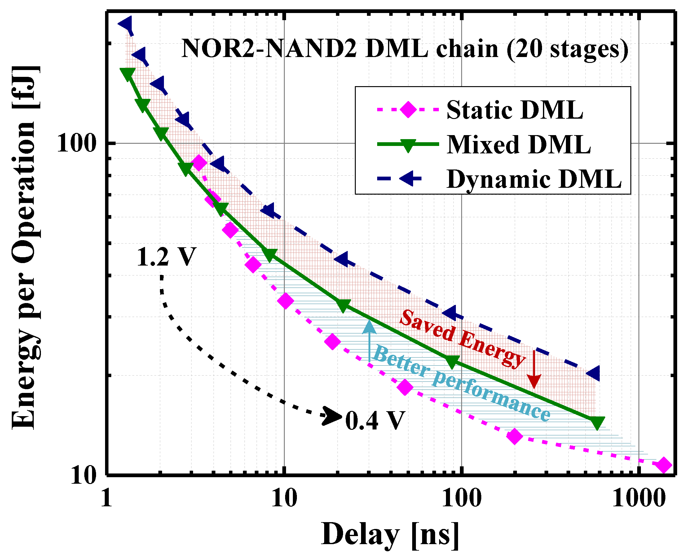
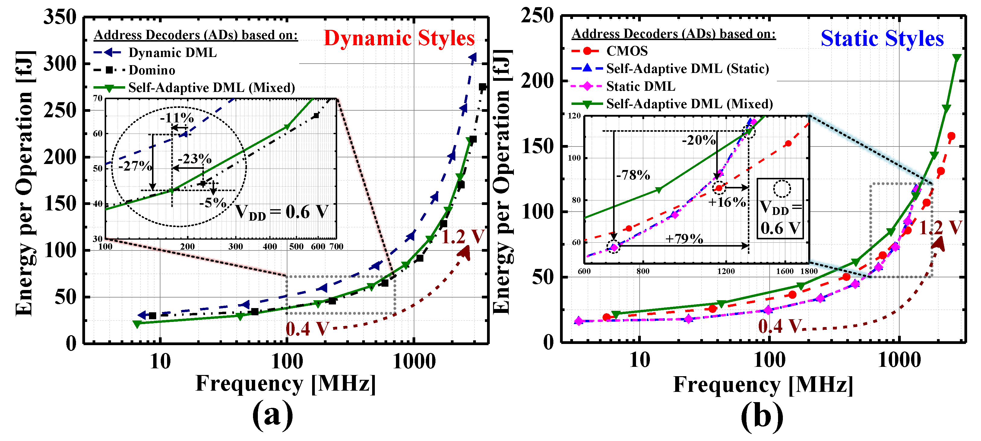
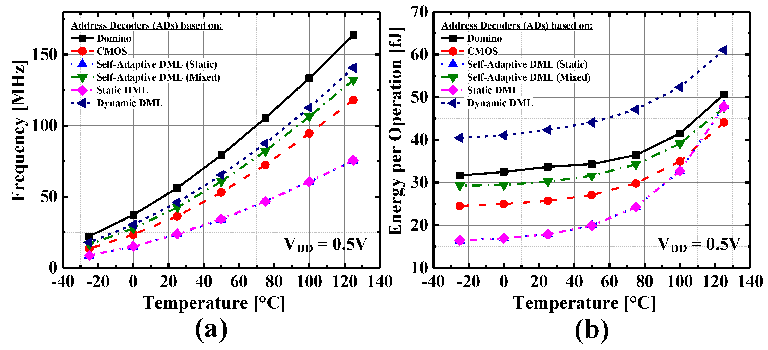
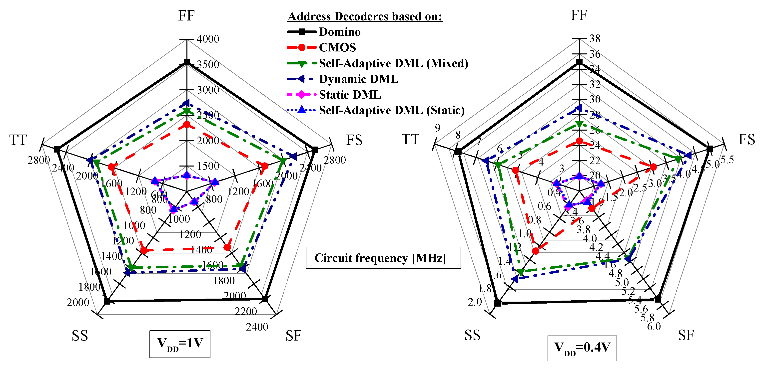
4. Results
5. Conclusions
Author Contributions
Funding
Conflicts of Interest
Abbreviations
| DML | Dual Mode Logic |
| SAAD | Self-Adaptive Address Decoder |
| AD | Address Decoder |
| TSMC | Taiwan Semiconductor Manufacturing Company |
| PUN | Pull-Up Network |
| PDN | Pull-Down Network |
| PTL | Pass Transistor Logic |
| IoT | Internet of Things |
References
- Alioto, M. Enabling the Internet of Things: From Integrated Circuits to Integrated Systems; Springer: Berlin, Germany, 2017. [Google Scholar]
- Chandrakasan, A.P.; Daly, D.C.; Finchelstein, D.F.; Kwong, J.; Ramadass, Y.K.; Sinangil, M.E.; Sze, V.; Verma, N. Technologies for ultradynamic voltage scaling. Proc. IEEE 2010, 98, 191–214. [Google Scholar] [CrossRef]
- Lanuzza, M.; Margala, M.; Corsonello, P. Cost-effective low-power processor-in-memory-based reconfigurable datapath for multimedia applications. In Proceedings of the 2005 International Symposium on Low Power Electronics and Design, San Diego, CA, USA, 8–10 August 2005; pp. 161–166. [Google Scholar] [CrossRef]
- Klinefelter, A.; Roberts, N.E.; Shakhsheer, Y.; Gonzalez, P.; Shrivastava, A.; Roy, A.; Craig, K.; Faisal, M.; Boley, J.; Oh, S.; et al. 21.3 A 6.45 μW self-powered IoT SoC with integrated energy-harvesting power management and ULP asymmetric radios. In Proceedings of the 2015 IEEE International Solid-State Circuits Conference-(ISSCC) Digest of Technical Papers, San Francisco, CA, USA, 22–26 February 2015; pp. 1–3. [Google Scholar] [CrossRef]
- Taco, R.; Levi, I.; Lanuzza, M.; Fish, A. Low voltage logic circuits exploiting gate level dynamic body biasing in 28 nm UTBB FD-SOI. Solid State Electron. 2016, 117, 185–192. [Google Scholar] [CrossRef]
- Myers, J.; Savanth, A.; Howard, D.; Gaddh, R.; Prabhat, P.; Flynn, D. 8.1 An 80 nW retention 11.7 pJ/cycle active subthreshold ARM Cortex-M0+ subsystem in 65 nm CMOS for WSN applications. In Proceedings of the 2015 IEEE International Solid-State Circuits Conference-(ISSCC) Digest of Technical Papers, San Francisco, CA, USA, 22–26 February 2015; pp. 1–3. [Google Scholar] [CrossRef]
- Calhoun, B.H.; Chandrakasan, A.P. Ultra-dynamic voltage scaling (UDVS) using sub-threshold operation and local voltage dithering. IEEE J. Solid State Circuits 2005, 41, 238–245. [Google Scholar] [CrossRef]
- Corsonello, P.; Frustaci, F.; Lanuzza, M.; Perri, S. Over/undershooting effects in accurate buffer delay model for sub-threshold domain. IEEE Trans. Circuits Syst. I Regul. Pap. 2014, 61, 1456–1464. [Google Scholar] [CrossRef]
- Lin, T.; Chong, K.S.; Chang, J.S.; Gwee, B.H. An Ultra-Low Power Asynchronous-Logic In-Situ Self-Adaptive VDD System for Wireless Sensor Networks. IEEE J. Solid State Circuits 2012, 48, 573–586. [Google Scholar] [CrossRef]
- Rabaey, J.M.; Chandrakasan, A.P.; Nikolić, B. Digital Integrated Circuits: A Design Perspective; Pearson Education, Inc.: Upper Saddle River, NJ, USA, 2003; Volume 7. [Google Scholar]
- McIntyre, H.; Arekapudi, S.; Busta, E.; Fischer, T.; Golden, M.; Horiuchi, A.; Meneghini, T.; Naffziger, S.; Vinh, J. Design of the two-core x86-64 AMD “Bulldozer” module in 32 nm SOI CMOS. IEEE J. Solid-State Circuits 2011, 47, 164–176. [Google Scholar] [CrossRef]
- Frustaci, F.; Lanuzza, M.; Zicari, P.; Perri, S.; Corsonello, P. Designing high-speed adders in power-constrained environments. IEEE Trans. Circuits Syst. II Express Briefs 2009, 56, 172–176. [Google Scholar] [CrossRef]
- Oklobdzija, V.G.; Montoye, R.K. Design-performance trade-offs in CMOS-domino logic. IEEE J. Solid State Circuits 1986, 21, 304–306. [Google Scholar] [CrossRef]
- Kursun, V.; Friedman, E.G. Domino logic with variable threshold voltage keeper. IEEE Trans. Very Large Scale Integr. Syst. 2003, 11, 1080–1093. [Google Scholar] [CrossRef] [Green Version]
- Frustaci, F.; Lanuzza, M.; Zicari, P.; Perri, S.; Corsonello, P. Low-power split-path data-driven dynamic logic. IET Circuits Devices Syst. 2009, 3, 303–312. [Google Scholar] [CrossRef]
- Akl, C.J.; Bayoumi, M.A. Single-phase SP-domino: A limited-switching dynamic circuit technique for low-power wide fan-in logic gates. IEEE Trans. Circuits Syst. II Express Briefs 2008, 55, 141–145. [Google Scholar] [CrossRef]
- Sung, R.J.H.; Elliott, D.G. Clock-logic domino circuits for high-speed and energy-efficient microprocessor pipelines. IEEE Trans. Circuits Syst. II Express Briefs 2007, 54, 460–464. [Google Scholar] [CrossRef]
- Liu, Z.; Kursun, V. Leakage power characteristics of dynamic circuits in nanometer CMOS technologies. IEEE Trans. Circuits Syst. II Express Briefs 2006, 53, 692–696. [Google Scholar] [CrossRef]
- Alioto, M.; Palumbo, G.; Pennisi, M. Understanding the effect of process variations on the delay of static and domino logic. IEEE Trans. Very Large Scale Integr. Syst. 2009, 18, 697–710. [Google Scholar] [CrossRef]
- Levi, I.; Kaizerman, A.; Fish, A. Low voltage dual mode logic: Model analysis and parameter extraction. Microelectron. J. 2013, 44, 553–560. [Google Scholar] [CrossRef]
- Kaizerman, A.; Fisher, S.; Fish, A. Subthreshold Dual Mode Logic. IEEE Trans. Very Large Scale Integr. Syst. 2013, 21, 979–983. [Google Scholar] [CrossRef]
- Yuzhaninov, V.; Levi, I.; Fish, A. Design Flow and Characterization Methodology for Dual Mode Logic. IEEE Access 2015, 3, 3089–3101. [Google Scholar] [CrossRef]
- Lanuzza, M.; De Rose, R.; Frustaci, F.; Perri, S.; Corsonello, P. Comparative analysis of yield optimized pulsed flip-flops. Microelectron. Reliab. 2012, 52, 1679–1689. [Google Scholar] [CrossRef]
- Fish, A.; Kaizerman, A.; Fisher, S.; Levi, I. Device and Method for Dual-Mode Logic. U.S. Patent 8,901,965,B2, 21 August 2014. [Google Scholar]
- Taco, R.; Levi, I.; Lanuzza, M.; Fish, A. An 88-fJ/40-MHz [0.4 V]–0.61-pJ/1-GHz [0.9 V] Dual-Mode Logic 8 × 8 bit Multiplier Accumulator with a Self-Adjustment Mechanism in 28-nm FD-SOI. IEEE J. Solid State Circuits 2019, 54, 560–568. [Google Scholar] [CrossRef]
- Shavit, N.; Stanger, I.; Taco, R.; Lanuzza, M.; Fish, A. A 0.8-V, 1.54-pJ/940-MHz Dual-Mode Logic-Based 16×16-b Booth Multiplier in 16-nm FinFET. IEEE Solid State Circuits Lett. 2020, 3, 314–317. [Google Scholar] [CrossRef]
- Levi, I.; Fish, A. Dual Mode Logic—Design for Energy Efficiency and High Performance. IEEE Access 2013, 1, 258–265. [Google Scholar] [CrossRef]
- Yavits, L.; Taco, R.; Shavit, N.; Stanger, I.; Fish, A. Dual Mode Logic Address Decoder. In Proceedings of the 2020 IEEE International Symposium on Circuits and Systems (ISCAS), Seville, Spain, 10–21 October 2020; pp. 1–5. [Google Scholar] [CrossRef]
- Stanger, I.; Shavit, N.; Taco, R.; Lanuzza, M.; Fish, A. Silicon Evaluation of Multimode Dual Mode Logic for PVT-Aware Datapaths. IEEE Trans. Circuits Syst. II Express Briefs 2020, 67, 1639–1643. [Google Scholar] [CrossRef]
- Brzozowski, I.; Zachara, L.; Kos, A. Designing Method of Compact n-to-2n Decoders. Int. J. Electron. Telecommun. 2013, 59, 405–413. [Google Scholar] [CrossRef] [Green Version]
- Ammar, Y.; Bdiri, S.; Derbel, F. An ultra-low power wake up receiver with flip flops based address decoder. In Proceedings of the 2015 IEEE 12th International Multi-Conference on Systems, Signals & Devices (SSD15), Mahdia, Tunisia, 16–19 March 2015; pp. 1–5. [Google Scholar] [CrossRef]
- Benini, L.; De Micheli, G.; Macii, E.; Sciuto, D.; Silvano, C. Asymptotic zero-transition activity encoding for address busses in low-power microprocessor-based systems. In Proceedings of the Great Lakes Symposium on VLSI, Urbana-Champaign, IL, USA, 13–15 March 1997; pp. 77–82. [Google Scholar] [CrossRef] [Green Version]
- Levi, I.; Fish, A. Dual Mode Logic: A New Paradigm for Digital IC Design; Springer Nature: Berlin, Germany, 2020. [Google Scholar]
- Levi, I.; Belenky, A.; Fish, A. Logical Effort for CMOS-Based Dual Mode Logic Gates. IEEE Trans. Very Large Scale Integr. Syst. 2014, 22, 1042–1053. [Google Scholar] [CrossRef]
- Levi, I.; Bass, O.; Kaizerman, A.; Belenky, A.; Fish, A. High Speed Dual Mode Logic Carry Look Ahead Adder. In Proceedings of the 2012 IEEE International Symposium on Circuits and Systems (ISCAS), Seoul, Korea, 20–23 May 2012; pp. 3037–3040. [Google Scholar] [CrossRef]


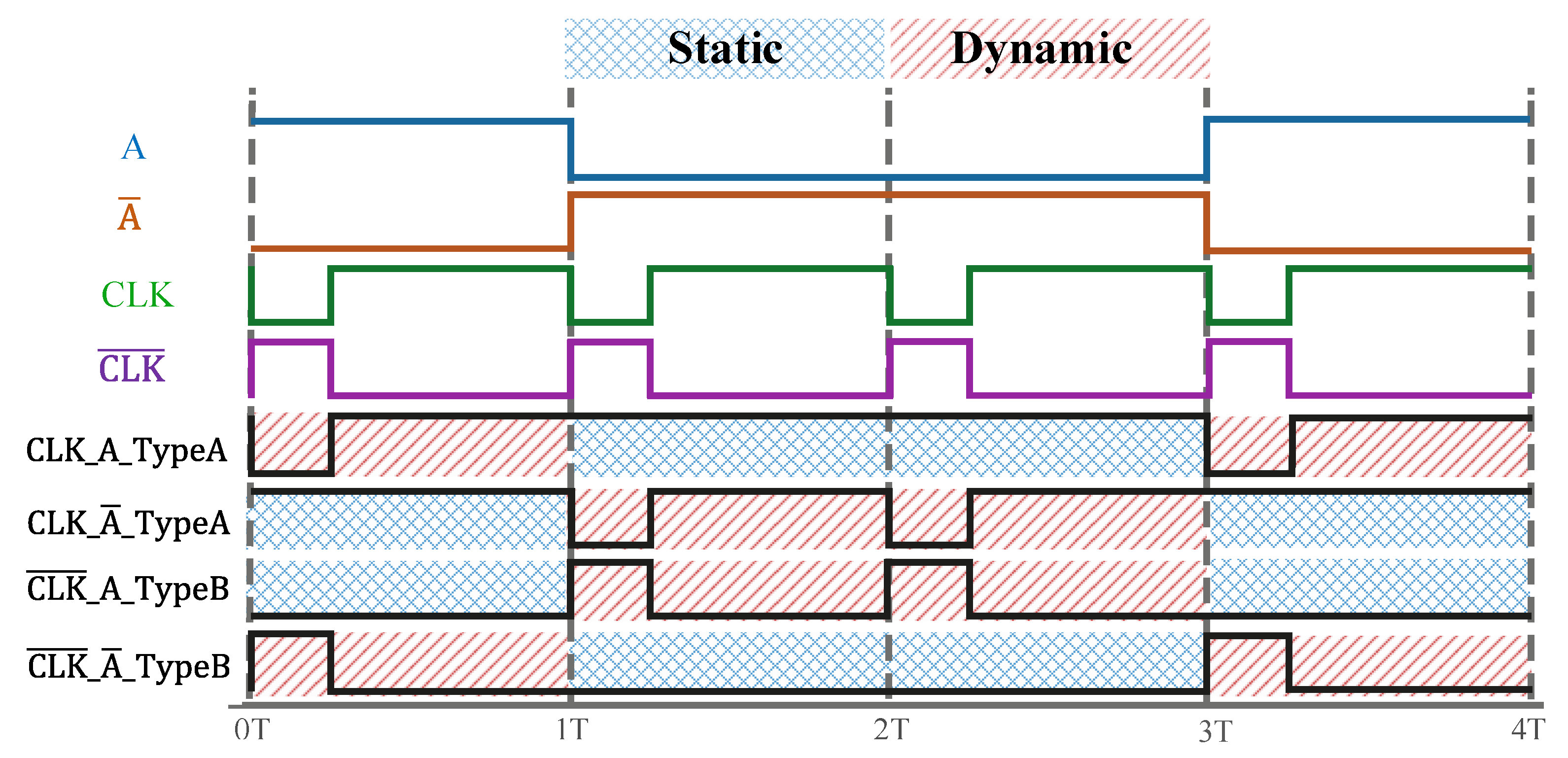
| State Topology | Block Input | A = logic “1” | A = logic “0” |
|---|---|---|---|
| DML Type-A | A | Dynamic Mode | Static Mode |
| Static Mode | Dynamic Mode | ||
| DML Type-B | A | Static Mode | Dynamic Mode |
| Dynamic Mode | Static Mode |
| Address Decoder | Number of Transistors | Area [μm2] |
|---|---|---|
| Self-Adaptive(Controllers) | 10,436 (84) | 10,531.96 (571.95) |
| DML | 10,352 | 9960.02 |
| Domino | 6264 | 9622.56 |
| CMOS | 8176 | 10,207.63 |
Publisher’s Note: MDPI stays neutral with regard to jurisdictional claims in published maps and institutional affiliations. |
© 2021 by the authors. Licensee MDPI, Basel, Switzerland. This article is an open access article distributed under the terms and conditions of the Creative Commons Attribution (CC BY) license (https://creativecommons.org/licenses/by/4.0/).
Share and Cite
Vicuña, K.; Mosquera, C.; Musello, A.; Benedictis, S.; Rendón, M.; Garzón, E.; Prócel, L.M.; Trojman, L.; Taco, R. Energy Efficient Self-Adaptive Dual Mode Logic Address Decoder. Electronics 2021, 10, 1052. https://doi.org/10.3390/electronics10091052
Vicuña K, Mosquera C, Musello A, Benedictis S, Rendón M, Garzón E, Prócel LM, Trojman L, Taco R. Energy Efficient Self-Adaptive Dual Mode Logic Address Decoder. Electronics. 2021; 10(9):1052. https://doi.org/10.3390/electronics10091052
Chicago/Turabian StyleVicuña, Kevin, Cristhopher Mosquera, Ariana Musello, Sara Benedictis, Mateo Rendón, Esteban Garzón, Luis Miguel Prócel, Lionel Trojman, and Ramiro Taco. 2021. "Energy Efficient Self-Adaptive Dual Mode Logic Address Decoder" Electronics 10, no. 9: 1052. https://doi.org/10.3390/electronics10091052