Article

Indirect Effective Controlled Split Source Inverter-Based Parallel Active Power Filter for Enhancing Power Quality

by
Poornima Udaychandra Panati
1,
Sridhar Ramasamy
1,
Mominul Ahsan
2,
Julfikar Haider
3 and
Eduardo M.G. Rodrigues
4,*
1
Department of Electrical Engineering, SRM Institute of Science and Technology, Kattankulathur 603203, Tamil Nadu, India
2
Department of Computer Science, University of York, Deramore Lane, York YO10 5GH, UK
3
Department of Engineering, Manchester Metropolitan University, John Dalton Building, Chester Street, Manchester M1 5GD, UK
4
Management and Production Technologies of Northern Aveiro—ESAN, Estrada do Cercal 449, Santiago de Riba-Ul, 3720-509 Oliveira de Azeméis, Portugal
*
Author to whom correspondence should be addressed.
Electronics 2021, 10(8), 892; https://doi.org/10.3390/electronics10080892
Submission received: 12 March 2021 / Revised: 29 March 2021 / Accepted: 6 April 2021 / Published: 8 April 2021
(This article belongs to the Special Issue 10th Anniversary of Electronics: Recent Advances in Power Electronics)

Abstract

:
The existing solutions for reducing total harmonic distortion (THD) using different control algorithms in shunt active power filters (SAPFs) are complex. This work proposes a split source inverter (SSI)-based SAPF for improving the power quality in a nonlinear load system. The advantage of the SSI topology is that it is of a single stage boost inverter with an inductor and capacitor where the conventional two stages with an intermediate DC-DC conversion stage is discarded. This research proposes inventive control schemes for SAPF having two control loops; the outer control loop regulates the DC link voltage whereas the inner current loop shapes the source current profile. The control mechanism implemented here is an effective, less complex, indirect scheme compared to the existing time domain control algorithms. Here, an intelligent fuzzy logic control regulates the DC link voltage which facilitates reference current generation for the current control scheme. The simulation of the said system was carried out in a MATLAB/Simulink environment. The simulations were carried out for different load conditions (RL and RC) using a fuzzy logic controller (FLC) and PI controllers in the outer loop (voltage control) and hysteresis current controller (HCC) and sinusoidal pulse width modulation (SPWM) in the inner loop (current control). The simulation results were extracted for dynamic load conditions and the results demonstrated that the THD can be reduced to 0.76% using a combination of SPWM and FLC. Therefore, the proposed system proved to be effective and viable for reducing THD. This system would be highly applicable for renewable energy power generation such as Photovoltaic (PV) and Fuel cell (FC).

1. Introduction

With the advent of power electronic converters, the power conversion for various applications has become quite easy. However, the power quality issues due to the nonlinear switching of power devices have become inevitable. Among all the power quality issues, the most prevalent one is the harmonics. Total harmonic distortion (THD) results in poor power factor, insulation failures, non-sinusoidal source, poor voltage profile, etc. The harmonic distortion in source voltage is very high when the power electronic interfaces relate to induction heating circuits, arc furnace, un-interruptible power supplies (UPS) [1,2]. To alleviate the impact of harmonics, filter circuits are used. In general, the inductor (L) and capacitor (C) form L-C passive filters which do not possess any static control [3]. Active power filters (APFs) [4] are embedded with control switches whose duty cycle is tuned to the amount of inclusion of LC values. The APF topology that is prevalently used in grid systems to compensate for the harmonic distortion have an energy storage component with an inverter. Many research works have been archived in proposing new topologies for the inverter or new control scheme of the inverter for compensating the harmonic distortion.
The inverter topology presently used are six-switch topologies in which the switches will be of MOSFETs or insulted gate bipolar transistor (IGBT). Kim [5] proposed a new hybrid active power filter topology in which the combination of MOSFETs and IGBTs were used. The hybrid switch usage helped in dealing with various combinations of high- and low-voltage, switching frequencies. The IGBT embedded inverter accounts for voltage compensation whereas the MOSFET was for current compensation. The above-discussed scheme, though advantageous, encounters more switching losses. Another breakthrough happened when Hirve et al. [6] and Barva et al. [7] proposed a three-phase, four-wire system, but there was additional control complexity in the system. Similarly, articles were published based on the reference signals generated for the control of shunt active power filter (SAPF) in either frequency domain or time domain algorithms [8,9]. In [10,11], synchronous reference frame theory and instantaneous PQ theory were used to generate the reference currents. Therefore, the THD was reduced to within the permissible limit, but the voltage across the DC link capacitor varied with respect to the transient conditions.
With the advent of multilevel inverter (MLI) topologies, the harmonic mitigation and pure sinusoidal waveform at inverter terminal output became pragmatic [12,13]. MLIs like cascaded H-bridge, diode clamped inverter, flying capacitor inverter and its control methods, applications, etc., were proposed [14,15]. Recently, a detailed review of modular multilevel converters and its control nuances were presented in [16]. A five-level cascaded H-bridge (CHB) was implemented using a space vector pulse width modulation technique [17], which was a complex scheme of producing PWM signals. In active power filters, instead of the conventional inverters, MLIs can be used but the PWM generation with greater driver units makes the compensation scheme very complex [18].
In recent years, single-stage inverters have gained more importance due to their reduced circuit complexity, less weight and smaller number of components. Peng introduced the Z-source inverter (ZSI), which comprised two sets of two passive elements, i.e., an inductor, a capacitor, and a diode connected to act as a buck/boost inverter [19]. All these topologies will have L-C impedance networks which facilitates the buck boost capability [20,21,22] and is combined with the inversion unit. The major drawbacks of these topologies are poor DC regulation and high complexity in designing the L-C network. Furthermore, achieving the shoot through mode to boost the voltage in single stage inverter is quite complex.
A split source inverter (SSI) is of unique topology, which uses only an inductor and a capacitor, and diode as the prime components [23]. Additionally, it does not utilize any extra switching state and the voltage across the bridge remains stable. The SSI topology utilizes the same states as voltage source inverter (VSI) with the same modulation schemes. This topology is a combination of boost converter merged with 3-φ VSI connected with the input inductor through diodes to the split points of the bridge inverter. With these advantages in mind, in this research work SSI topology has been chosen to compensate the harmonic currents in the line.
Various controller schemes for active power filters have been reported in the research arena. In a typical control scheme, the grade of harmonic impact is measured and PWM (pulse width modulation) pulses for the inverter are generated in such a way that the inverter feeds harmonic currents into the line to negate the existing harmonic currents. The control algorithm aids in maintaining the desired point of common coupling (PCC) voltage, harmonic current elimination, and load balancing of the nonlinear loads. On the other hand, achieving voltage regulation at the PCC and unity power factor control cannot be achieved simultaneously. In all, the SAPF compensation scheme involves four essential facets and they are harmonic reference current generation, synchronization, DC link voltage regulation and current control. A detailed survey on SAPF has been archived in the literature [24]. Conventional proportional integral (PI) controllers for the voltage and current control were used in [25,26] to regulate the harmonic current and the DC voltage. However, to achieve versatility in the PI controller, an accurate model of the system should be known, which is difficult to obtain with the given nonlinearity, load disturbances and parameter variations. The fuzzy logic controller (FLC) is one of the intelligent control methods and even without a precise linear mathematical model, it can perform well.
The FLC-based shunt APF was reported in [27], where the reference current generation was carried out using P-Q theory and the FLC was used for current injection and DC voltage regulation. Here, the complexity lies in framing the rules with the membership functions. In [28], dynamic characteristics of VSI based SAPF for varying loads were discussed. In [29], synchronous reference theory was used to develop reference current generation for seven level cascaded H-bridge inverter (SLCHB), seven level modular multilevel converter (SLMMC)-based SAPF was employed to reduce the harmonics to 4%. A hybrid predictive fuzzy logic (HPFL)-based technique was used to reduce harmonics where the predictive part was used for compensating current generation and fuzzy logic for voltage regulation [30]. Another study designed a low-cost hybrid shunt active power filter using PI/fuzzy for generating reference current and to regulate DC link capacitor voltage and switching pulses were generated by using an adaptive fuzzy hysteresis current controller (A-F-HCC) [31]. In [32], maximum power point tracking (MPPT) and DC link voltage regulation were carried out using a fuzzy logic controller. All these systems mentioned above used time domain control algorithms to generate current references. A comparison of the controllers for VSI based SAPF has been discussed with respect to the reduction of harmonics in [33]. A sliding mode controller (SMC) for shunt APF for improving power factor was discussed in [34], whereas a THD of 1.45% was produced by the designed system with complex reference current generation method. The maximum development of a shunt APF for improving power quality with predator-prey based firefly optimization was well presented in [35]. However, in this work, the authors developed an optimization technique for a normal voltage source inverter (VSI)-based APF and complex controller computation methods. Single- and three-phase PUC-5 inverter systems were reported in [36] where the converter had two equally regulated separate DC links for the APF application.
From the detailed literature, it is inferred that the quest on proposing simple but versatile control schemes for SAPF is still in demand. Additionally, the choice of inverter topology should achieve the required compensation. This research paper proposes an inventive FLC-aided SSI for SAPF. The fuzzy controller in the outer loop provides good DC regulation and reduced harmonics. SSI is advantageous with reduced components, DC link capacitor voltage and high voltage gain with conventional switching states and shorter commutation path. The paper is so organized that Section 2 deals with analysis of SSI and modelling of the SSI. The design of controllers for SSI-based SAPF has been explored in Section 3. Section 4 presents the results obtained from dynamic and steady state conditions of nonlinear loads. Finally, the conclusions are presented in Section 5.

2. System Description

Figure 1 presents the SSI-based SAPF system architecture using a block diagram. An AC source with a balanced nonlinear load (NLL) was introduced. An insulted gate bipolar transistor (IGBT)-based SSI with a DC bus capacitor was used for the SAPF and its AC side was connected in parallel across the loads or point of common coupling (PCC). The gating pulses to the inverter bridge were generated by employing a current controller over the reference and sensed supply currents as an indirect current control. It had two control loops, a voltage control loop and a current control loop. The voltage control loop regulates the DC link capacitor voltage (V2). The sensed DC link capacitor voltage was compared with the reference DC link voltage (V2ref) and the error was fed to a PI/fuzzy controller. The output of the PI controller was the amplitude of the current, which was used to derive the reference current. A phase-locked loop (PLL) is used to extract the source voltage. The reference current was compared with the source current in the current control loop for generating gate signals for the switches (T1 to T6) of the SSI in the SAPF.

2.1. Analysis of SSI

The basic circuit of 3-φ SSI shown in Figure 2A in this section uses the same B6 bridge of the traditional VSI combined with an impedance network to implement the boost capability. SSI comprises of two passive elements, an inductor and a capacitor. Three diodes are connected in series with the input inductor with the nodes of each leg in bridge as shown in Figure 2A. L is discharged only in one state and charges the capacitor (i.e., the DC link capacitor) as shown in the Figure 2B, a–h. Inductor L can be charged in any of the six active states and a zero state. During the other zero state, L discharges through the antiparallel diode connected across the upper switches. SSI has connected to a linear load and a diode rectifier load according to the IEC62040-3 standard.
According to the modes of operation, the circuit operates as boost converter in continuous conduction mode where switches in the inverter are in conduction state (i.e.,) L will be charged for a period of T o n and discharging for a period T o f f .
The duty cycle δ   given by Equation (1):
δ = T o n T o n + T o f f
where Ton = charging time and Toff = discharging time.
For Figure 2i, the sinusoidal pulse width modulation (SPWM) technique was applied, the mathematical equations of SPWM modulation schemes are discussed where the duty cycle δ , minimum and maximum duty cycle are δ m i n , δ m a x respectively and its average value of duty cycle δ a v of modulation scheme can be determined by Equation (2):
δ ( θ ) = 1 2 { 1 m   s i n ( θ ) }
The inverter is 3φ (i.e.,) 7 π 6   θ   11 π 6 , where θ is the angle of interval and modulation index m is shown with respect to minimum value and maximum value (Equations (3) and (4)):
δ m i n = 1 2 + 1 4 m
δ m a x = 1 2 + 1 2 m
The average duty cycle (i.e.,) inductor gets charged is given by δ a v (Equation (5)):
δ a v = 1 2 + 3 3 4 π m
The average normalized inverter voltage V p V 1 is given by Equation (6):
V p V 1 = 4 π 2 π 3 3 m
where V1 is the DC input Voltage and Vp is the voltage applied across the inverter bridge. The fundamental output phase voltages Vo1 can be calculated as (Equation (7)):
V o 1 V 1 = 2 π m 2 π 3 3 m
For the selection of the capacitor and inductor value, both the frequency components due to the switching cycle as well as duty cycle has been considered. The high frequency ripple for the inductor current Δ I L H and the capacitor voltage Δ V P H are defined by Equations (8) and (9), respectively:
Δ I L H = δ V 1 f s L
Δ V P H = ( 1 δ ) I d c f s C
where Idc is the input current.
The capacitor current ripple I C l and inductor voltage ripple V L l   of low frequency are defined by (Equations (10) and (11)), respectively, assuming constant inductor current and inverter voltage:
| V L l | = ( 1 δ ( θ ) ) V p
| I C l | = ( 1 δ ( θ ) ) I d c
To calculate the low frequency ripple components, only the fundamental terms of | V L l | and | I C l | , the Fourier series of δ ( θ ) is considered, where ΔIL is the allowable ripple current and ΔVp is the allowable voltage ripple are the combination of low frequency component and high frequency component. The capacitor and inductor values are calculated from Equations (12) and (13):
L w m V p 6 π f 1 Δ I L + δ m a x V 1 2 f s Δ I L
C w m I d c 6 π f 1 Δ V p + ( 1 δ m i n ) I d c 2 f s Δ V p
where fs is the switching frequency and f1 is the fundamental frequency, w is a constant given by Equation (14):
w = 3 3 8 π

2.2. Modeling of SSI

The average modelling SSI-based SAPF is essential for designing the controller parameters [9,10]. The SSI state space equations can be engraved by dividing each switching time period Ts, into two interval ton and toff (refer Figure 2). During ton, the charging period of L and C is supplying the load during active switching. In toff, L is discharging, and C is charging during that zero state, performing as an intermediate state for transfer of energy. Choosing state variables x1 = iL, x2 = V2 of the SSI-based shunt SAPF (see Figure 2) and its state space equation of two interval ton and toff are represented by Equations (15) and (16):
d i L d t = V 1 L r L i L L
d V 2 d t = i i n v C                                                                 interval   t o n
d i L d t = V 1 L r L i L L V 2 L
d V 2 d t = i L C                                                                 interval   t o f f
where r L is the internal resistance and i i n v is the current through the bridge.

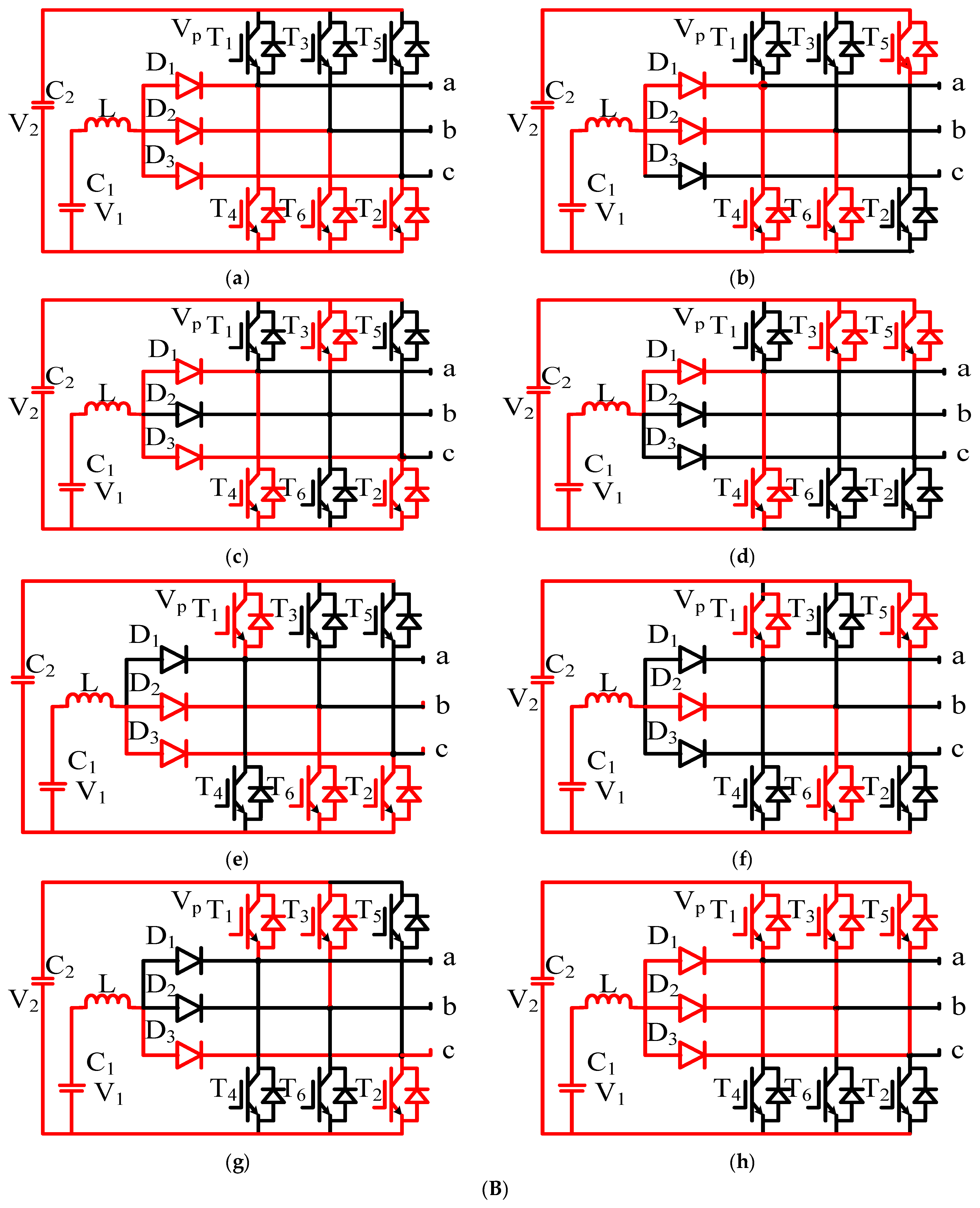
3. SSI Based SAPF with Controllers

The three phase SSI-based SAPF with controllers are illustrated in Figure 3. From this figure, it is observed that the two DC link voltages of capacitors C1 and C2 are summed to attain the measured DC link voltage V2. This Vdc is compared with DC link reference voltage Vdc* to obtain the voltage error, which is applied to single FLC/PI controller to produce the control signal. This generated control signal and synchronization of supply sin θ from the phase-locked loop (PLL) are multiplied to obtain the reference current of the APF is*. Now, the measured current is from the supply is compared with the is* to generate the reference voltage signal. This reference voltage is compared with multiple carrier signals with integrated voltage balancing to generate the PWM pulse for gating switches of an inverter. The inverter must inject the current at PCC to compensate the current (current controller), reduce the THD, improve the power factor and balance the capacitors voltage (FLC/PI controller) during the SAPF operated at non-linear load condition. Now, the current equation of the given model is defined by Equation (17):
i s + i f = i L
where i f is the current through the filter at the point of common coupling.

3.1. Design of PI Controller

The proportional-integral (PI) is a traditional controller that is used to retain sinusoidal output current, to maintain near-unity and fast implementation of the power factor. The proportional and integral gains are Kp and Ki, respectively. The difference between reference voltage and output voltage is the error signal. The values of Kp and Ki are 0.9 and 500 respectively are set by tuning of the controller using the Ziegler–Nicholas method.

3.2. Design of FLC

The fuzzy logic controller is one of the non-linear and intelligent controllers. The rules of the FLC are derived from the system parameters without the mathematical model of the system. The FLC converts a linguistic control strategy based on expert knowledge into an automatic control strategy, which makes the system stable. The FLC consists of three parts namely, fuzzification, inference system, defuzzification. The fuzzy variables are expressed in terms of membership functions. The Sugeno method of fuzzification was used where the output was numerical values. The membership functions of error and change in error of the proposed model are depicted in Figure 4a,b, respectively.
In this proposed system, Gaussian membership functions were selected as the inputs. The voltage errors of the capacitor within the inverter were given as the input to FLC. Then, FLC output was multiplied to synchronize the supply voltage signal sinθ via the phase-locked loop (PLL) and the reference current of APF. Then, is was compared with is* to make the reference voltage signal (refer Figure 3). This reference voltage was compared with the carrier signals, which are integrated with voltage balancing to generate the PWM pulse for gating the switches of SSI. The current from the SSI is injected at PCC to compensate the current.
The fuzzy sets were NB (negative big), NS (negative small), Z (zero), PS (positive small), PM (positive medium) and PB (positive big), respectively. The assortment of FLC 49 rules were to be wholly contingent on dynamic deeds of the proposed APF (see Table 1). Finally, the defuzzification-weighted average method was involved.

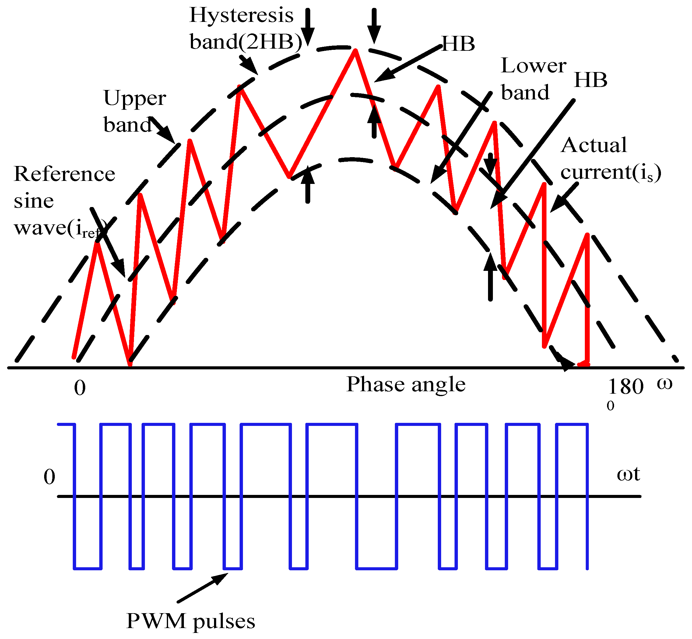
3.3. Hysteresis Current Controller (HCC)

This method is simpler, and the implementation does not require complex circuits or processors. The graphical representation of HCC for designed filter is illustrated in Figure 5. The HCC method appears in such a way as to compel the current to remain within a hysteresis band (HB) when the switch is ON/OFF. When the error reaches a fixed HB magnitude, the switches will operate within the backslash limits. The control laws with respect to the power switches of the SSI of the APF are as follows.
HBmin ≤ iref − is ≤ HBmax, none of the power switches are closed.
Iaref − Isa, Ibref − Isb, Icref − Isc>HBmax, T1, T3 and T5 are closed.
iref − is <HBmin, T4, T6 and T2 are closed. Isa, Isb, Isc are source currents.
The optimal operating frequency (ω) with desired HB can be written as
ω = 0.5 Π V 2 V 1 HB × L f
where V1 is the source voltage and V2 is the DC link capacitor voltage, HB is the hysteresis band and Lf is the inverter side inductance.

4. Results and Discussion

This section deals with the simulation results of the proposed three-phase SSI-based SAPF with various controllers at different load operating conditions. In this proposed system, diode bridge rectifier (DBR) with RL and RC were utilized as the nonlinear loads. The experiments were performed under source and load balanced conditions as shown in Figure 6. To validate the robustness and dynamic responses of the proposed SSI-based SAPF, a step change load was introduced with the non-linear loads. During hysteresis current controlling, a sudden load variation was applied at a time period of 0.05 s where the total simulation time was 0.1 s. For SPWM technique, a sudden load variation was introduced at 0.5 s while the total simulation time was set at 1.0 s.
The specifications of SSI-based SAPF is catalogued in Table 2. Here, HCC was employed as an inner loop for the source current profile and reduce the THD of it, whereas the PI controller and FLC were used as the outer loop for regulating its DC link voltages. Figure 7 indicates the simulated responses of the source current and THD of the power system without SAPF at different load conditions.
From these results, it was evident that the THDs of the power system without filter at RL load and RC Load were 23.05% and 23.45%, respectively, that were much higher than IEEE standard limit of 5%. To reduce the THD and refine the source current, a SAPF using three phase split source inverter was introduced in the proposed power system design.

4.1. Hysteresis Current Controller (HCC) with Different Controllers for Voltage Regulation

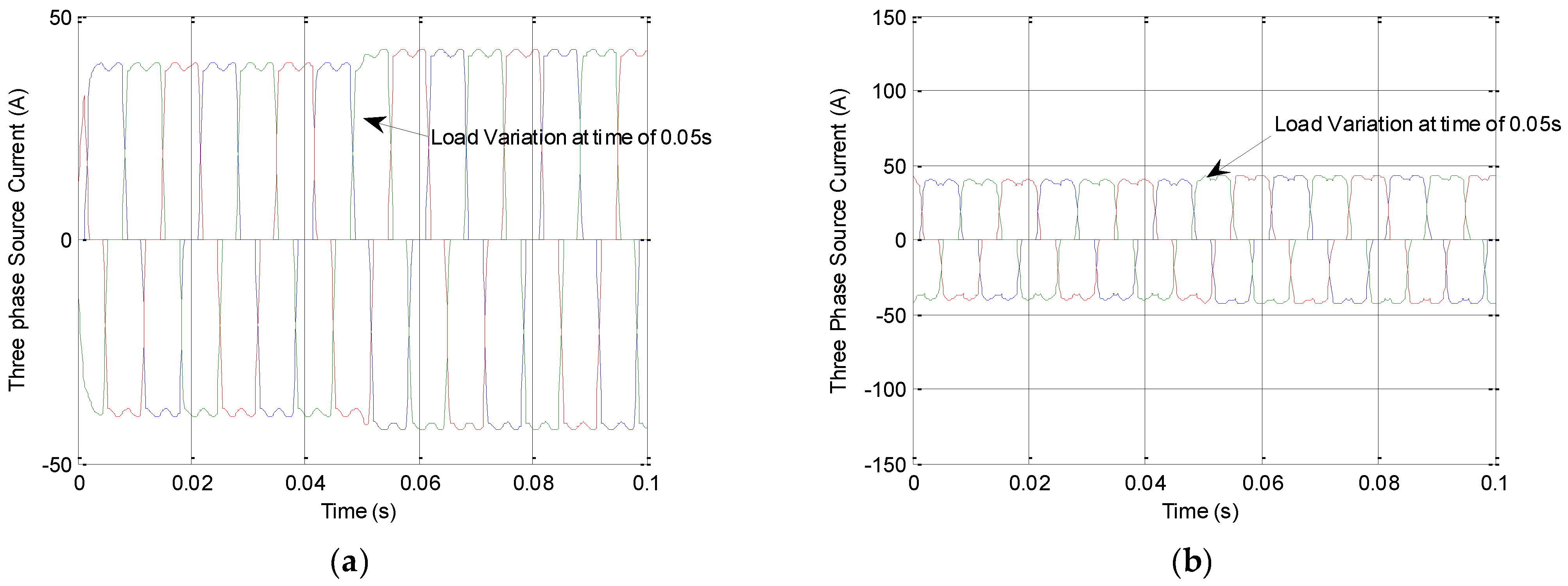
4.1.1. Case 1 for HCC: PI and FLC Controllers with RL Loads

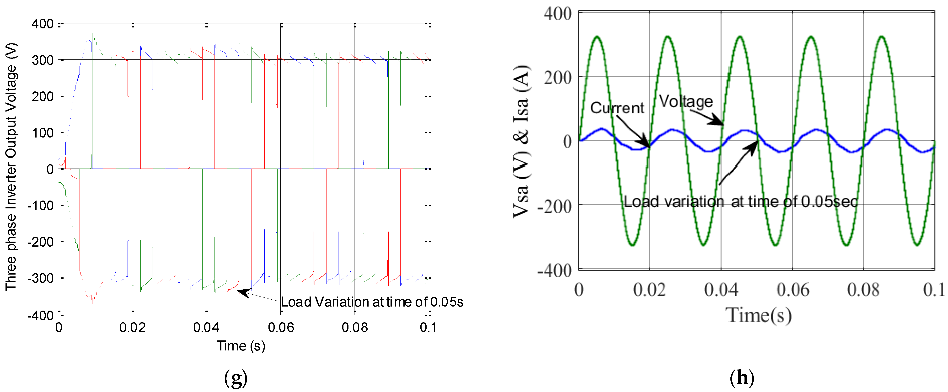
Figure 8a–c shows the change in source current, load current and compensation current, for RL load when SAPF was connected. It was found that the proposed model when subjected to dynamic load changes, the DC link voltage profile having a peak overshoot with a voltage of 387 V before it settled at a time of 0.15 s and reached to a voltage of 347 V with zero steady state error as shown in Figure 8e. At 0.05 s, the load was increased by 5 Ω, and it was observed that the controller had null overshoots, zero steady state error, and zero settling time. Hence, 
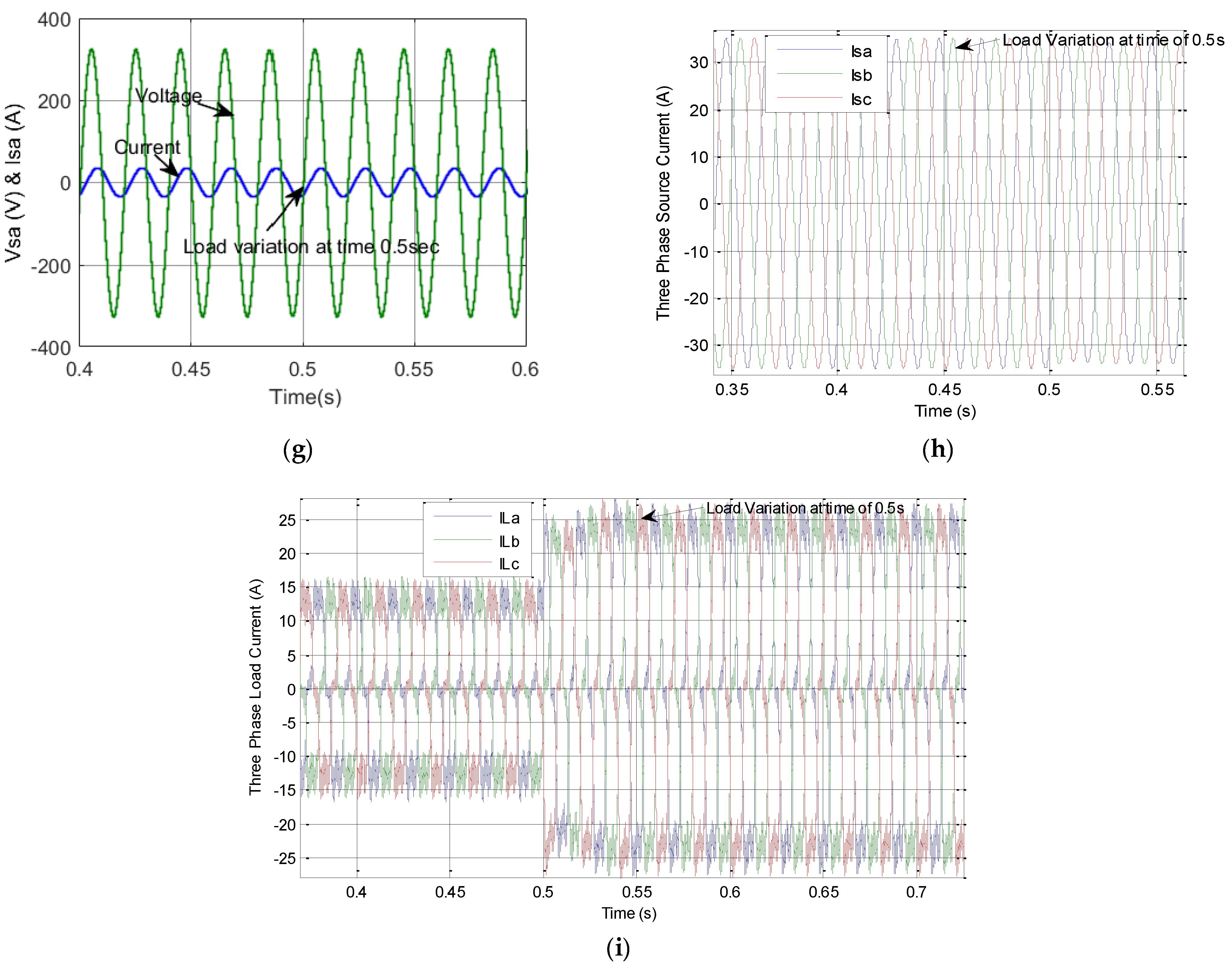
Figure 8g shows the three-phase line voltage of three-phase split source inverter. Figure 8h shows the source current profile in phase with source voltage. The source current reached almost near to its current profile with a harmonic percentage of 4.47% which is shown in Figure 8d.
Figure 9a–c shows the change in source current, load current and compensation current for the RL load when the SAPF was connected. When the proposed system was subjected to load changes of the diode rectifier bridge, the DC link voltage profile had a peak overshoot with a voltage of 387 V before it settled at a time of 0.13 s and reached a voltage of 327 V with zero steady state error as shown in Figure 9e. At 0.05 s, the load was increased by 5 Ω and it was observed that the controller had null overshoots, zero steady state error, and zero settling time. Figure 9g shows the three-phase line voltage of the three-phase split source inverter with 315 V. Figure 9h shows the source current profile in phase with the source voltage. The source current reached almost near to its current profile with a harmonic percentage of 4.46%, which is shown in Figure 9d.
From these results, it was evident that the proposed model with HCC and FLC displayed proficient performance at DBR based RL loads. Furthermore, DC link voltages were settled at a quick settling time/zero steady state error and null peak overshoots with a voltage of 327 V. The source current reached almost near to its current profile with HCC and FLC with less distortion in its waveform and source current harmonics were reduced to 4.46%.

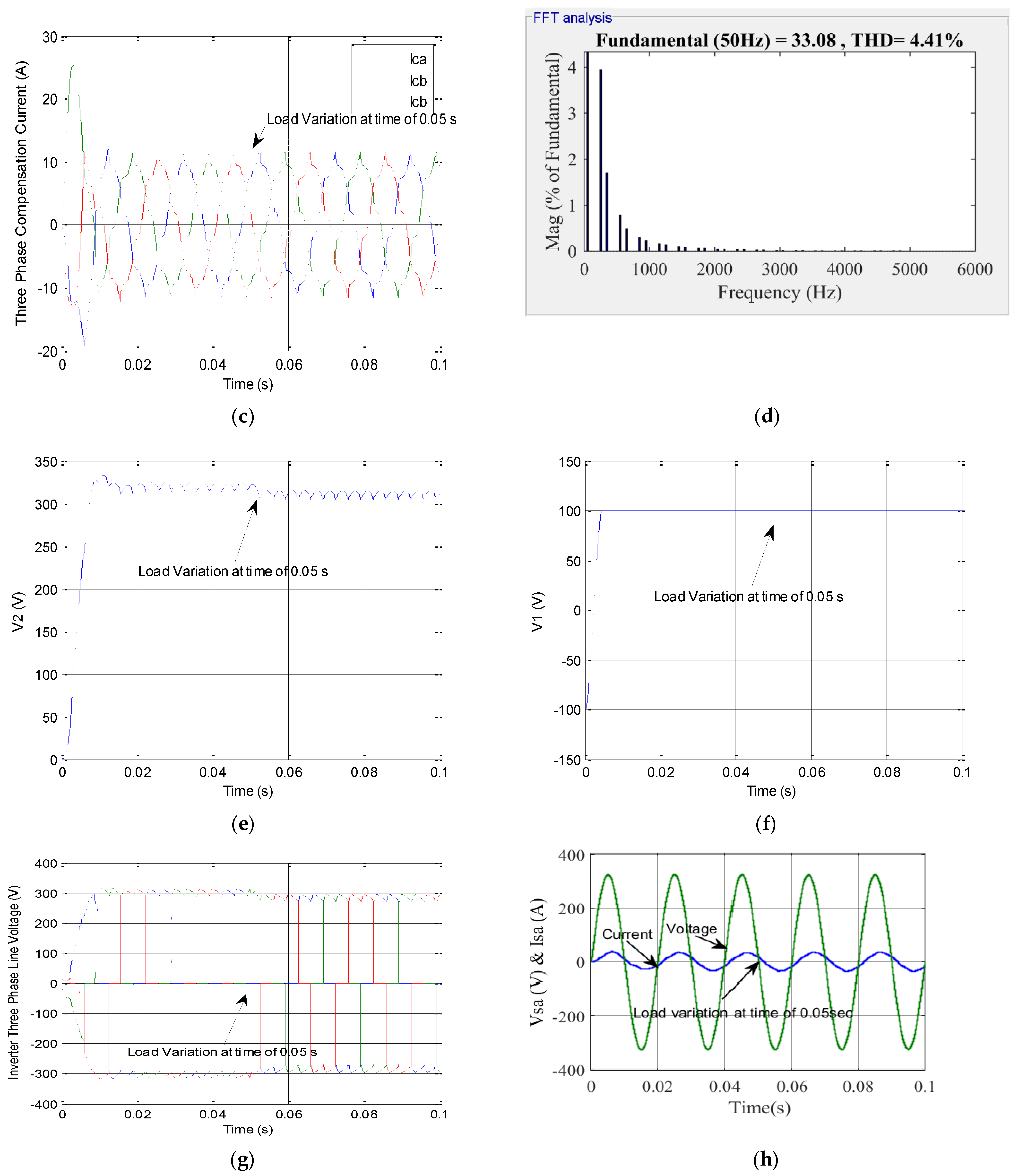
4.1.2. Case 2 for HCC: PI and FLC Controllers with RC Loads

The simulation results illustrated in Figure 10a–c include the source current, load current and compensation current for the RC loads when SAPF was connected. The PI control scheme involves regulation of the DC link voltage. The DC link voltage showed a small peak overshoot before it reached the steady state voltage of 337 V, as shown in Figure 10e. The DC link voltage had zero steady state error, null overshoots and zero settling time during the step change in load variation with a minimized ripple voltage. In this case, the SAPF has been introduced to compensate harmonics and has reduced the THD from 23.45% to 4.41%. The source current near to the current profile indicated a reduction in harmonics to 4.41% as shown in Figure 10d. 
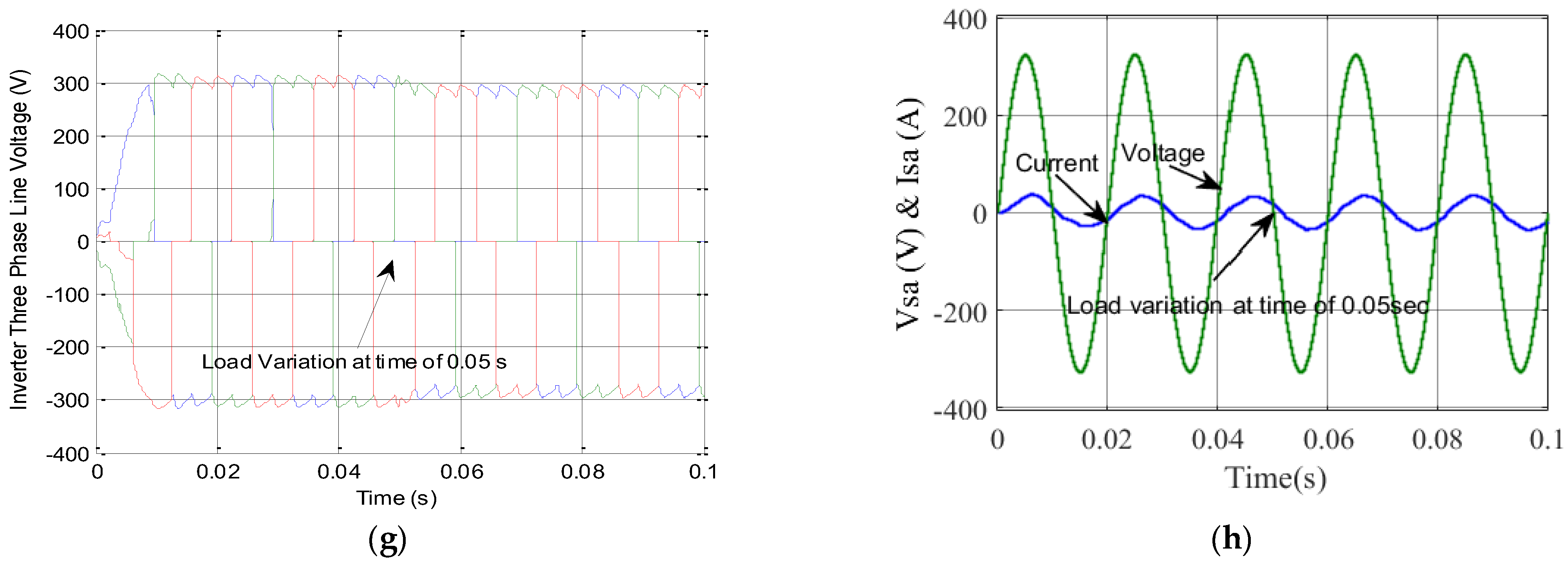
Figure 10g shows the output line voltage of the three-phase split source inverter. Figure 10h shows that supply voltage and source current were almost in phase with the power factor.
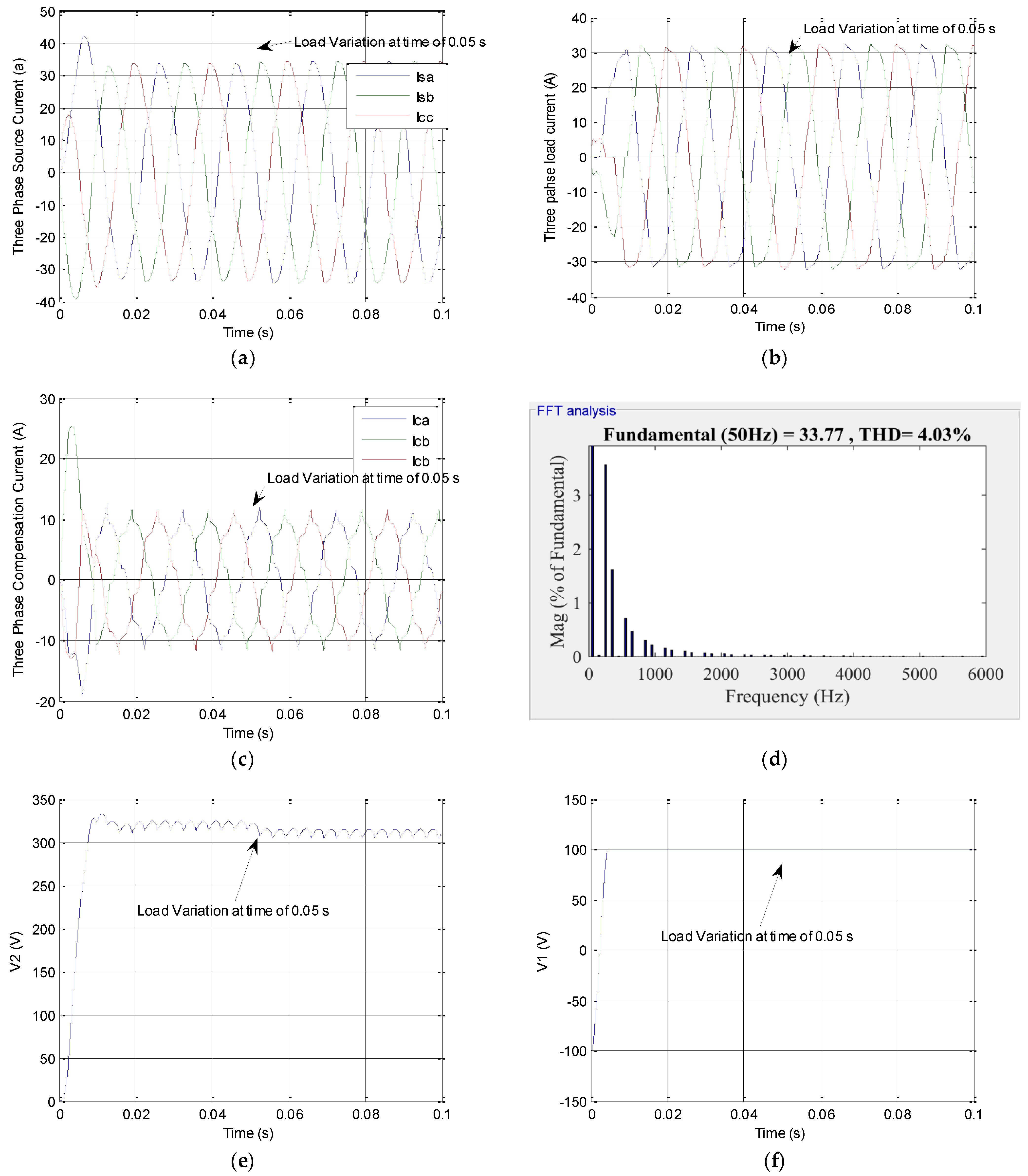
Figure 11a–c show the source current, load current, compensation current. It was observed that when there was a sudden change in load at 0.05 s, it had zero steady state error at 327 V with a minimized ripple voltage which is shown in Figure 11e. The source current near to the current profile indicated a reduction in harmonics by 4.03%, as shown in Figure 11d. Figure 11g shows the output line voltage of the three-phase split source inverter. Figure 11h shows that supply voltage and source current were almost in phase. When the FLC controller was connected in the outer loop it performed well because the overall system was a nonlinear system. The DC link voltage remained constant. The source current harmonics were found to be 4.46% and 4.03% for various loads using the FLC over PI controller with a near to source current profile. Thus, the results proved the system dynamic performance during transient condition.

4.2. SPWM with Different Controllers for DC Link Voltage Regulation

4.2.1. Case 1 for SPWM: PI and FLC Controllers with RL Loads

It was observed that when the controllers for DC link voltage regulation was varied, the total harmonic distortion has been reduced to IEEE standard limit of 5%. When the proposed model treated with a different controller in the inner loop, percentage of THD reduction has been verified. Figure 12a–c shows the change in source current, load current and compensation current. It was further observed that the proposed model when subjected to dynamic load changes, the DC link voltage profile showed a peak overshoot with a voltage of 387 V before it settled at a time of 0.2 s and reached a voltage of 300 V with zero steady state error, as shown in Figure 12e. At 0.5 s, the load was increased by 5 Ω and it was observed that the controller had null overshoots and zero steady state error. Figure 12f shows the three-phase line voltage of three phase split source inverter. Figure 12g shows the source current profile in phase with the source voltage. The source current reached almost near to its current profile with a THD of 1.03% as shown in Figure 12d.
Figure 13a–c shows the source current, load current, and compensation current when SAPF relates to SPWM and FLC Controller. Figure 13e shows the DC link voltage profile showing a peak overshoot of 447 V and it reached a voltage of 350 V with zero steady state error. When there is a sudden change in load, the FLC controller had null overshoots and zero steady state error. Figure 13f shows the line-to-line voltage of three phase split source inverter. Figure 13g shows the source current profile in phase with the source voltage. The source current reached almost near to its current profile with a harmonic percentage of 0.76% as shown in Figure 13d. 
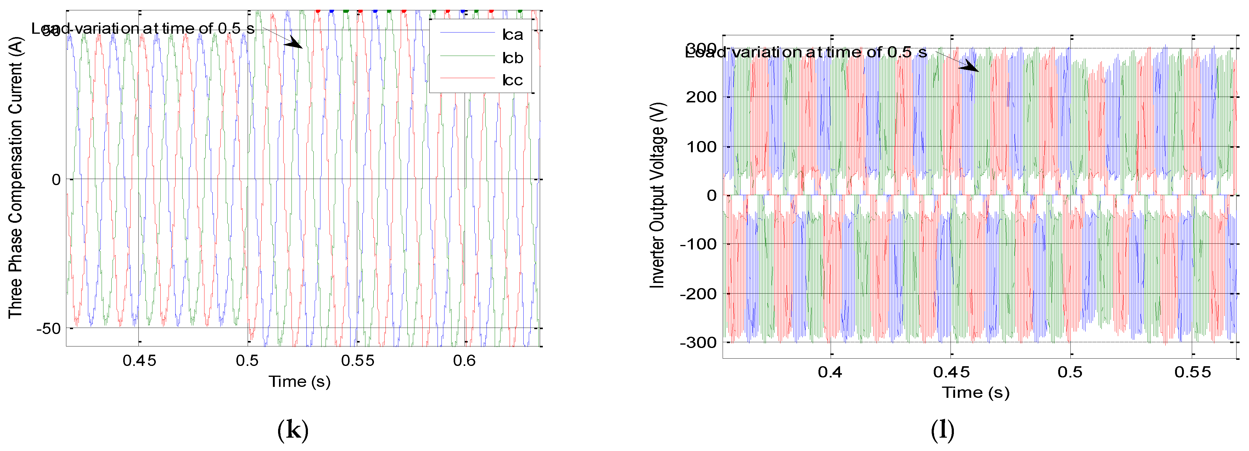
Figure 13j shows that the input inductor current has been increased and a small voltage dip during a transient period of 0.5 s. Figure 13k,l,h show the zoomed graphs of source current, load current and compensation current of load variation at the time of 0.5 s. When the FLC controller was connected to the outer loop and SPWM controller to the inner loop, controller where the DC link voltage remained constant, the source current harmonics was found to be 0.76% for FLC over PI controller with near to the source current profile and power factor near to the unity. Thus, these results proved the system dynamic performance during transient condition.

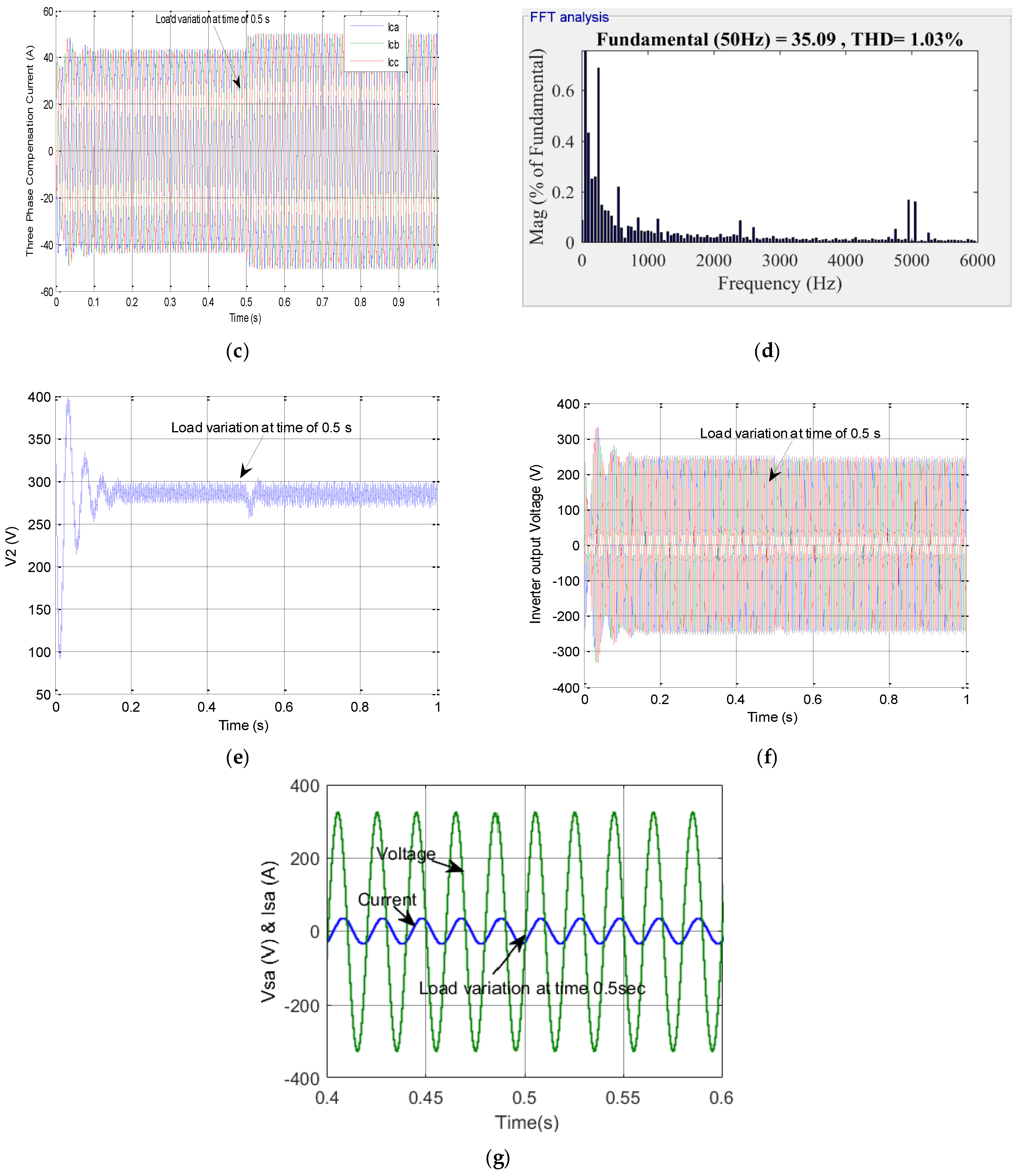
4.2.2. Case 2 for SPWM: PI and FLC Controllers with RC Loads

The difference in the DC link voltage regulation with PI and FLC controllers with SPWM are presented Figure 14 and Figure 15. Figure 14a–c shows the source current, load current and compensation current when SSI is connected as SAPF. The DC link voltage showed a peak overshoot before it reached the steady state voltage of 347 V as shown in Figure 14e. At 0.5 s, when there was a sudden change in load, the DC link voltage had zero steady state error, null overshoots and zero settling time with a minimized ripple voltage. The source current was near to the current profile with a reduction of harmonics by 1.00% as shown in Figure 14d. Figure 14f shows the output line voltage of split source inverter. Figure 14g shows that supply voltage of 315 V and source current are almost in phase with the power factor near to unity.
Figure 15a–c shows the change in source current, load current and compensation current. The DC link voltage profile showed a peak overshoot with a voltage of 410 V before it settled at a time of 0.14 s and reached to a voltage of 347 V at 0.5 s with zero steady state error, as shown in Figure 15e. It was observed that the fuzzy logic controller had null overshoots, zero steady state error and a small voltage dip during a transient period of 0.5 s. Figure 15f shows the three-phase line voltage of three phase split source inverter. Figure 15g shows the source current profile in phase with the source voltage. The source current reached almost near to its current profile with a harmonic of 0.72% as shown in Figure 15d. hence, Figure 15h,i are zoomed waveforms of the source current and load current at 0.5 s. The FLC controller was connected to the outer loop and SPWM controller to the inner loop, controller where the DC link voltage remained constant. The source current harmonics was found to be 0.72% for FLC over PI controller with near to the source current profile and a power factor near to the unity. Thus, these results proved the system dynamic performance during transient condition.

4.3. Comparative Analysis and Discussion

In order to analyse the performance of the proposed approach, statistical analysis of the case studies with a shunt active power filter configuration using various approaches is illustrated in Table 3. From the results, it was evident that the proposed model with SAPF demonstrated proficient performance at DBR based RC and RL loads where DC link voltages were settled in quick time with almost zero steady state error and minimized ripple voltage for FLC controller compared to the PI controller with a sudden load variation at 0.5 s. Owing to the nonlinearity in the total system, fuzzy logic controller performed well compared to the PI controller for RL and RC loads. Furthermore, the inner current controllers in HCC and SPWM were replaced with outer loop controllers. The source current harmonics had almost the source current profile and the power factor was near unity with lower distortion factor.
The load values were changed dynamically, and the automatic regulation was investigated for the developed controller. From the results obtained based on the simulations of different case studies under different load conditions, it can be concluded that the proposed system is robust enough to accommodate any sudden load variations. Therefore, the system could bring a sustainable and simple solution for automatic regulation of load nonlinearity.
From Table 3, it was found that the designed SAPF through SPWM and fuzzy logic control aided SSI showed better performance with significantly reduced THD down to 0.76% for the RL load and 0.72% for RC load. When compared the HCC and PI controller with the SPWM and FLC, the later one demonstrated almost six times lower THD, which would significantly contribute towards improving the power quality.
From Table 4, it can be concluded that topologies implemented requires a greater number of switches [29], and PWM techniques which are used to generate gate pulses are complicated. The DC link capacitors rating required was high in all other topologies. In [35,36], the reference current generation led to the complexity of the structure. It can be observed that indirect effective controlled SSI-based SAPF showed less THD, less distortion and good DC voltage regulation under transient conditions.
In this work, the simulations were focused on reduction of THD and overall system losses due to the harmonics created by nonlinear loads which are used in domestic as well as industrial applications. A substantial increase in the harmonics might lead to energy losses, the life span of the electrical equipment might decrease and derating of the electrical equipment. To avoid these drawbacks, a three phase SSI-based SAPF for current harmonic compensation has been proposed. When identifiable harmonics are present, the best solution is to suppress the harmonics at the source side. The dynamic performance of the SSI-based SAPF was designed with an indirect effective control to suppress the harmonics from the source side by injecting the harmonic current at PCC. The fuzzy-based strategies regulating the DC link capacitor voltage made it simple, robust and less susceptible to system transients.

5. Conclusions

An effective indirect control scheme for SSI-based SAPF with the fuzzy logic control technique and with sinusoidal pulse width modulation was successfully designed. The performance of the fuzzy logic controller (FLC) was validated by comparing it with the conventional PI controller and it was found that FLC reduced the THD to 0.76%, which was lower than the THD obtained by the PI controller (1.03%). The inverter current control was accomplished by the SPWM scheme, which outperformed the hysteresis control with respect to the total harmonic distortion. The whole system was tested for dynamic load variations under balanced condition, and it was found that the combination of fuzzy and SPWM remained to be superior (THD 0.76%) when compared with the PI and hysteresis control (4.47%). The potential barrier of the proposed system might have reliability issues with respect to the single stage but, given the control complexity issues, the suggested scheme is believed to be the most preferred and viable. It should also be mentioned that the system was validated using extensive modelling and simulations under different scenarios. However, in the future, an experimental setup should be developed for further validation and implementation in real life situations.

Author Contributions

All authors have equal contribution to prepare and finalise the manuscript Conceptualization: P.U.P., S.R., M.A. and J.H.; methodology: P.U.P., S.R., M.A. and J.H.; software: P.U.P. and S.R.; validation: P.U.P., S.R., M.A., J.H. and E.M.G.R.; formal analysis: P.U.P., S.R., M.A., J.H. and E.M.G.R.; investigation: P.U.P., S.R., M.A., J.H. and E.M.G.R.; resources: P.U.P. and S.R.; data curation: P.U.P. and S.R.; writing—original draft preparation: P.U.P. and S.R.; writing—review and editing: P.U.P., S.R., M.A., J.H. and E.M.G.R.; visualization: P.U.P., S.R., M.A., J.H. and E.M.G.R.; supervision: S.R., M.A., J.H. and E.M.G.R.; project administration: P.U.P. and S.R. All authors have read and agreed to the published version of the manuscript.

Funding

This research received no external funding.

Data Availability Statement

The data presented in this study are available in the article.

Acknowledgments

The authors would like to thank the team of Manchester Met University for their support for this research work and preparation of the manuscript.

Conflicts of Interest

The authors declare no conflict of interest.

References

  1. Khlifi, K.; Haddouk, A.; Hlaili, M.; Mechergui, H. Harmonic Pollution Caused by Non-Linear Load: Analysis and Identification. Int. J. Energy Environ. Eng. 2018, 12, 510–517. [Google Scholar]
  2. Ko, A.; Swe, W.; Zeya, A. Analysis of harmonic distortion in non-linear loads. Int. J. Comput. Internet Manag. 2011, 19, 661–666. [Google Scholar]
  3. Singh, M.; Mahapatra, S. Implementation of Passive Filters for Harmonics Reduction. Int. J. Adv. Sci. Technol. 2015, 78, 1–12. [Google Scholar] [CrossRef]
  4. El-Habrouk, M.; Darwish, M.K.; Mehta, P. Active power filters: A review Article. IEE Proc. Electr. Power Appl. 2000, 147, 403–413. [Google Scholar] [CrossRef]
  5. Kim, S.; Enjeti, P.N. A New Hybrid Active Power Filter (APF) Topology. IEEE Trans. Power Electron. 2002, 17, 48–54. [Google Scholar]
  6. Hirve, S.; Chatterjee, K.; Fernandes, B.G.; Imayavaramban, M.; Dwari, S. PLL-less active power filter based on one cycle control for compensating unbalanced loads in three phase four wire system. IEEE Trans. Power Deliv. 2007, 22, 2457–2465. [Google Scholar] [CrossRef] [Green Version]
  7. Barva, A.V.; Bhavsar, P.R. Design and Simulation of Split-Capacitor Based Three-Phase Four-Wire Shunt Active Power Filter. In Proceedings of the IEEE International Conference on Recent Trends in Electronics Information & Communication Technology (RTEICT), Bangalore, India, 19–20 May 2017. [Google Scholar]
  8. Hoon, Y.; Radzi, M.A.M.; Hassan, M.K.; Mailah, N.F. Control Algorithms of Shunt Active Power Filter for Harmonics Mitigation: A Review. Energies 2017, 10, 2038. [Google Scholar] [CrossRef] [Green Version]
  9. Kumar, R.; Bansal, H.O. Shunt active power filter: Current status of control techniques and its integration to renewable energy sources. Sustain. Cities Soc. 2018, 42, 574–592. [Google Scholar] [CrossRef]
  10. Chourasiya, S.; Agarwal, S. A review: Control Techniques for Shunt Active Power Filter for Power Quality Improvement from Non-Linear Loads. Int. Electr. Eng. J. 2015, 6, 2028–2032. [Google Scholar]
  11. Singh, H.; Kour, M.; Thanki, D.V.; Kumar, P. A Review on Shunt Active Power Filter Control Strategies. Int. J. Eng. Technol. 2018, 7, 121–125. [Google Scholar] [CrossRef]
  12. Rodriguez, J.; Lai, J.S.; Peng, F.Z. Multilevel inverters: A survey of topologies, controls, and applications. IEEE Trans. Ind. Electron. 2002, 49, 724–738. [Google Scholar] [CrossRef] [Green Version]
  13. Halim, W.A.; Ganeson, S.; Azri, M.; Azam, T.N.A.T. Review of multilevel inverter topologies and its applications. J. Telecommun. Electron. Comput. Eng. 2016, 8, 51–56. [Google Scholar]
  14. Waware, M.; Agarwal, P. A Review of Multilevel Inverter Based Active Power Filter. Int. J. Comput. Electr. Eng. 2011, 3, 196–205. [Google Scholar] [CrossRef]
  15. Nabae, H.A.A.; Takahashi, I. A New Neutral-Point-Clamped PWM Inverter Technology. IEEE Trans. Ind. Appl. 1981, 1A-17, 518–523. [Google Scholar] [CrossRef]
  16. Dekka, A.; Wu, B.; Fuentes, R.L.; Perez, M.; Zargari, N.R. Evolution of topologies, modeling, control schemes, and applications of modular multilevel converters. IEEE J. Emerg. Sel. Top. Power Electron. 2017, 5, 1631–1656. [Google Scholar] [CrossRef]
  17. Massoud, A.M.; Finney, S.J.; Cruden, A.J.; Williams, B.W. Three-phase, three-wire, five-level cascaded shunt active filter for power conditioning, using two different space vector modulation techniques. IEEE Trans. Power Deliv. 2007, 22, 2349–2361. [Google Scholar] [CrossRef]
  18. Rajasekar, S.; Senthilkumar, A.; Kumar, Y.S.; Ajay-D-VimalRaj, P. Power quality enhancement using cascaded multilevel inverter-based shunt hybrid active power filter. Int. J. Eng. Sci. Technol. 2012, 3, 37–46. [Google Scholar] [CrossRef] [Green Version]
  19. Peng, F.Z. Z-source inverter. IEEE Trans. Ind. Appl. 2003, 39, 504–510. [Google Scholar] [CrossRef]
  20. Siwakoti, Y.; Town, G.; Loh, P.C.; Blaabjerg, F. Y-source inverter. In Proceedings of the 2014 IEEE 5th International Symposium on Power Electronics for Distributed Generation Systems (PEDG), Galway, Ireland, 24–27 June 2014; pp. 1–6. [Google Scholar]
  21. Abdelhakim, A. Analysis and modulation of the buck-boost voltage source inverter (bbvsi) for lower voltage stresses. In Proceedings of the 2015 IEEE International Conference on Industrial Technology (ICIT), Seville, Spain, 17–19 March 2015; pp. 926–934. [Google Scholar]
  22. Gao, F.; Loh, P.; Blaabjerg, F.; Teodorescu, R.; Vilathgamuwa, D. Component- minimized buck-boost voltage source inverters. In Proceedings of the 2007 IEEE Industry Applications Annual Meeting, New Orleans, LA, USA, 23–27 September 2007; pp. 2311–2318. [Google Scholar]
  23. Abdelhakim, A.; Mattavelli, P.; Spiazzi, G. Three-phase split-source inverter (SSI): Analysis and modulation. IEEE Trans. Power Electr. 2015, 31, 7451–7461. [Google Scholar] [CrossRef]
  24. Hoon, Y.; Radzi, M.A.M.; Zainuri, M.A.A.M.; Zawawi, M.A.M. Shunt active power filter: A review on phase synchronization control techniques. Electronics 2019, 8, 791. [Google Scholar] [CrossRef] [Green Version]
  25. Hinduja, M.; Rathi, M.K.; Christa, S.J.; Prabha, N.R. PI Control of Multi Level Inverter Based Shunt Active Power Filter for Harmonic Mitigation in Three Phase Systems. In Proceedings of the 2015 International Conference on Circuits, Power and Computing Technologies [ICCPCT-2015], Nagercoil, India, 19–20 March 2015. [Google Scholar]
  26. Ye, S.; Zhang, Y.; Xie, L.; Lu, H. Shunt Active Power Filter Based on Proportional Integral and Multi Vector Resonant Controllers for Compensating Nonlinear Loads. J. Electr. Comput. Eng. 2018, 1–11. [Google Scholar] [CrossRef] [Green Version]
  27. Saad, S.; Zellouma, L. Fuzzy logic controller for three-level shunt active filter compensating harmonics and reactive power. Electr. Power Syst. Res. 2009, 79, 1337–1341. [Google Scholar] [CrossRef]
  28. Singh, G.; Singh, A.; Mitra, R. A simple fuzzy logic based robust active power filter for harmonics minimization under random load variation. Electr. Power Syst. Res. 2006, 77, 1101–1111. [Google Scholar] [CrossRef]
  29. Narasimhulu, V.; Kumar, D.V.A.; Babu, C.S. Fuzzy Logic Control of SLMMC-Based SAPF Under Nonlinear Loads. Int. J. Fuzzy Sets 2020, 22, 428–437. [Google Scholar] [CrossRef]
  30. Fahmy, A.M.; Abdelslam, A.K.; Lotfy, A.A.; Hamad, M.; Kot, A. A Four Leg Shunt Active Power Filter Predictive Fuzzy Logic Controller for Low-Voltage Unbalanced-Load Distribution Networks. J. Power Electron. 2018, 18, 573–587. [Google Scholar]
  31. Mishra, A.K.; Ray, P.K.; Mallick, R.K.; Mohanty, A.; Das, S.R. Adaptive fuzzy controlled hybrid shunt active power filter for power quality enhancement. Neural Comput. Appl. 2021, 33, 1435–1452. [Google Scholar] [CrossRef]
  32. Kumara, R.; Bansal, H.O.; Agrawal, H.P. Development of fuzzy logic controller for photovoltaic integrated shunt active power filter. J. Intell. Fuzzy Syst. 2019, 36, 6231–6243. [Google Scholar] [CrossRef]
  33. Pedapenki, K.K.; Gupta, S.P.; Pathak, M.K. Comparison of PI & fuzzy logic controller for shunt active power filter. In Proceedings of the 2013 IEEE 8th International Conference on Industrial and Information Systems, Peradeniya, Sri Lanka, 17–20 December 2013; pp. 42–47. [Google Scholar] [CrossRef]
  34. Ullah, M.A.I. Sliding mode control for performance improvement of shunt active power filter. SN Appl. Sci. 2019, 1, 531. [Google Scholar] [CrossRef] [Green Version]
  35. Mahaboob, J.S.; Ajithan, S.K. Optimal design of shunt active power filter for power quality enhancement using predator-prey based firefly optimization. Swarm Evol. Comput. 2019, 44, 522–533. [Google Scholar] [CrossRef]
  36. Vahedi, H.; Shojaei, A.A.; Dessaint, L.A.; Al-Haddad, K. Reduced DC-Link Voltage Active Power Filter Using Modified PUC5 Converter. IEEE Trans. Power Electron. 2018, 33, 943–947. [Google Scholar] [CrossRef]
  37. Imam, A.A.; Kumar, R.S.; Al-Turki, Y.A. Modeling and Simulation of a PI Controlled Shunt Active Power Filter for Power Quality Enhancement Based on P-Q Theory. J. Electron. 2020, 9, 637. [Google Scholar] [CrossRef]
  38. Teja, B.R.; Krishna, B.R.; Gowtham, V.; Chakravarthi, M. Control Algorithm of Shunt Active Power Filter For Harmonic Mitigation Using Indirect Current Control Technique. Int. J. Electr. Eng. Technol. (IJEET) 2018, 9, 37–48. [Google Scholar]
  39. Sundaram, E.; Venugopal, M. On design and implementation of three phase three level shunt active power filter for harmonic reduction using synchronous reference frame theory. Int. J. Electr. Power Energy Syst. 2016, 81, 40–47. [Google Scholar] [CrossRef]
Figure 1. Block diagram of SSI-based SAPF for the three-phase, three-wire system.
Electronics 10 00892 g001
Figure 2. (A) Topology of SSI (B) (ah) Modes of operation of SSI with inductor charging and discharging.
Electronics 10 00892 g002aElectronics 10 00892 g002b
Figure 3. Circuit diagram of Three-phase SSI-based SAPF connected to the supply and non-linear load.
Electronics 10 00892 g003
Figure 4. Sugeno method FLC structure with membership functions. (a) Error in voltage (e), (b) change in error voltage (ce).
Electronics 10 00892 g004
Figure 5. Graphical representation of fixed band hysteresis current controller (HCC).
Electronics 10 00892 g005
Figure 6. Simulation of experimental conditions employed in this study.
Electronics 10 00892 g006
Figure 7. Simulated responses of the source current in the power system without SAPF for (a) RL load and (b) RC load.
Electronics 10 00892 g007
Figure 8. Simulated responses of three-phase SSI-based SAPF connected at the diode rectifier bridge (DRB)-RL load HCC and PI controller, (a) supply current, (b) load current, (c) compensation current, (d) THD, (e) V2 DC link voltage, (f) V1 DC link voltage, (g) SSI output voltage and (h) source voltage (Vsa) and source current (Isa) of phase A.
Electronics 10 00892 g008aElectronics 10 00892 g008b
Figure 9. Simulated responses of three phase SSI-based SAPF connected at DRB—RL load with HCC and FLC: (a) Supply current, (b) load current, (c) compensation current, (d) THD, (e) V2 DC link voltage, (f) V1 DC link voltage, (g) SSI output voltage and (h) source voltage (Vsa) and source current (Isa) of Phase A.
Electronics 10 00892 g009aElectronics 10 00892 g009b
Figure 10. Simulated responses of three phase SSI-based SAPF connected at DRB RC load with HCC and PI controller. (a) Supply current, (b) load current, (c) compensation current, (d) THD, (e) V2 DC link voltage, (f) V1 DC link voltage, (g) SSI output voltage and (h) source voltage (Vsa) and source current (Isa) of phase A.
Electronics 10 00892 g010aElectronics 10 00892 g010b
Figure 11. Simulated responses of three phase SSI-based SAPF connected at DRB RC load with HCC cum FLC: (a) Supply current, (b) load current, (c) compensation current, (d) THD, (e) V2 DC link voltage, (f) V1 DC link voltage, (g) SSI output voltage and (h) source voltage (Vsa) and source current (Isa) of phase A.
Electronics 10 00892 g011aElectronics 10 00892 g011b
Figure 12. Simulated responses of three phase SSI-based SAPF connected at DRB RL load with SPWM and PI controller: (a) Supply current, (b) load current, (c) compensation current, (d) THD, (e) V2 DC links voltage, (f) SSI output voltage and (g) source voltage (Vsa) and source current (Isa) of phase A.
Electronics 10 00892 g012aElectronics 10 00892 g012b
Figure 13. Simulated responses of three phase SSI-based SAPF connected at DRB RL load with SPWM and FLC controller: (a) Supply current, (b) load current, (c) compensation current, (d) THD, (e) V2 DC links voltage, (f) SSI output voltage (g) source voltage (Vsa) and source Current (Isa) of Phase A, (h) Zoomed source current, (i) zoomed load current, (j) inductor current, (k) zoomed compensation current and (l) zoomed inverter output voltage.
Electronics 10 00892 g013aElectronics 10 00892 g013bElectronics 10 00892 g013c
Figure 14. Simulated responses of three phase SSI-based SAPF connected at DRB RC load with SPWM and PI controller, (a) Supply current, (b) load current, (c) compensation current, (d) THD, (e) V2 DC links voltage (f) SSI output voltage and (g) source voltage (Vsa) and source current (Isa) of phase A.
Electronics 10 00892 g014aElectronics 10 00892 g014b
Figure 15. Simulated responses of three phase SSI-based SAPF connected at DRB RC load with SPWM and FLC controller, (a) Supply current, (b) load current, (c) compensation current, (d) THD, (e) V2 DC links voltage, (f) SSI output voltage, (g) source voltage (Vsa) and source current (Isa) of phase A, (h) zoomed source current and (i) zoomed load current.
Electronics 10 00892 g015aElectronics 10 00892 g015b
Table 1. Fuzzy rules for the proposed shunt active power filter (SAPF).
Electronics 10 00892 i001Error in Voltage (e)PBPMPSZNSNMNB
Electronics 10 00892 i002Change in Error Voltage (ce)
PBNMNMNMNMNMNSZ
PMNBPMPMNBNSNMNB
PSPSPMPSPMPSPSPM
ZNBNMNMPMNBPMNB
NSZZPBPBPBPMPB
NMNSZZNBPBNBPB
NBZPSPSPBNBNSPB
Table 2. Specifications of three phase SSI Based SAPF used for the simulation.
ParametersValue
Source Voltage (Vs)230 V (Peak Value)
Source Frequency (f)50 Hz
Inductor (L)6 mH
DC link capacitor voltages (V1 & V2)100 V, 347 V
DC bus capacitor (C1 & C)60 µF & 360 µF
Switching frequency (fs)2 kHz
Filter inductor (Lf)2 mH
Load inductor (LL)2 mH
Diode bridge rectifier RL Load10 Ω, 70 mH
Diode bridge rectifier RC Load10 Ω, 100 µF
Table 3. THD analyses of the proposed model at different load operating conditions with different controllers.
Load Type/Active Power FilterTHD (%)
RL LoadRC Load
System without SAPF23.0523.45
HCC and PI controller4.474.41
HCC and FLC4.464.03
SPWM and PI controller1.031.00
SPWM and FLC0.760.72
Table 4. THD analysis of the proposed inverter with other topologies with only RL load.
SAPF with Different TopologiesTHD (%)
PI (%)FLC (%)
SLCHB [29]4.854.68
SLMMC [29]4.294.01
3-Φ VSI [37]1.18-
3-Φ VSI with indirect current control technique [38]0.90-
3-Φ VSI With SRF [39]1.06-
3-Φ SSI [Proposed]1.030.76
Publisher’s Note: MDPI stays neutral with regard to jurisdictional claims in published maps and institutional affiliations.

