Article

Analysis of Electrothermal Effects in Devices and Arrays in InGaP/GaAs HBT Technology

by
Vincenzo d’Alessandro
1,*,
Antonio Pio Catalano
1,
Ciro Scognamillo
1,
Lorenzo Codecasa
2 and
Peter J. Zampardi
3
1
Department of Electrical Engineering and Information Technology, University Federico II, 80125 Naples, Italy
2
Department of Electronics, Information, and Bioengineering, Politecnico di Milano, 20133 Milan, Italy
3
Qorvo, Inc., Newbury Park, CA 91320, USA
*
Author to whom correspondence should be addressed.
Electronics 2021, 10(6), 757; https://doi.org/10.3390/electronics10060757
Submission received: 3 February 2021 / Revised: 10 March 2021 / Accepted: 18 March 2021 / Published: 23 March 2021
(This article belongs to the Special Issue Electrothermal Effects in Semiconductor Devices/Circuits)

Abstract

:
In this paper, the dc electrothermal behavior of InGaP/GaAs HBT test devices and arrays for power amplifier output stages is extensively analyzed through an efficient simulation approach. The approach relies on a full circuit representation of the domains, which accounts for electrothermal effects through the thermal equivalent of the Ohm’s law and can be solved in any commercial circuit simulator. In particular, the power-temperature feedback is described through an equivalent thermal network automatically obtained by (i) generating a realistic 3-D geometry/mesh of the domain in the environment of a numerical tool with the aid of an in-house routine; (ii) feeding the geometry/mesh to FANTASTIC, which extracts the network without performing simulations. Nonlinear thermal effects adversely affecting the behavior of devices/arrays at high temperatures are included through a calibrated Kirchhoff’s transformation. For the test devices, the thermally-induced distortion in IV curves is explained, and the limits of the safe operating regions are identified for a wide range of bias conditions. A deep insight into the electrothermal behavior of the arrays is then provided, with particular emphasis on the detrimental nonuniform operation. Useful guidelines are offered to designers in terms of layout and choice of the ballasting strategy.

1. Introduction

Gallium arsenide (GaAs) heterojunction bipolar transistors (HBTs) are the dominant technology for handset power amplifier (PA) design by virtue of their power density, cut-off frequency, and efficiency [1]. However, designing rugged circuits with GaAs HBT devices requires extra care because of strong electrothermal (ET) effects arising from (i) low thermal conductivity of the substrate, (ii) lateral heat confinement by mesa isolation, and (iii) high operating currents. Thermal-aware design methodologies relying on suitable ET simulation tools are highly desired to alleviate or avoid performance and reliability degradation. Unfortunately, the choice of the simulation approach is challenging. Full 3-D ET device simulations based on the finite-element method (FEM), e.g., with Atlas from Silvaco or Sentaurus from Synopsys, are computationally onerous or even unviable when dealing with complex structures like practical transistor arrays and packages.
A more efficient, yet accurate enough, approach is based on the generation and solution of a SPICE-compatible purely-electrical macrocircuit that accounts for ET effects by means of the thermal equivalent of the Ohm’s law (TEOL). In this macrocircuit, the power-temperature feedback is included through an equivalent thermal network (ETN, an electrical circuit relying on the TEOL), the components of which can be optimized in a pre-processing stage with the aid of 3-D thermal-only FEM simulations. A key part of this strategy is implementing an analytical transistor model as a subcircuit, in which the temperature-sensitive parameters are allowed to vary during the simulation run thanks to the TEOL (e.g., [2,3,4]). We adopted such an approach—based on in-house models for individual transistors—to examine the dc and transient ET behavior of devices/circuits for a large variety of technologies and applications, namely, single- and multi-finger silicon-on-glass (SOG) bipolar transistors [5,6,7]; output arrays of PAs in InGaP/GaAs HBT technology, yet with relevant approximations in describing the geometry of the devices [8]; basic analog blocks, like simple current mirrors [9,10], differential pairs [11,12], and cascode amplifiers [13] in many bipolar technologies (GaAs, SOG, and silicon-germanium); vertical double-diffused silicon-carbide MOS transistors with a multicellular pattern [14].
In our earlier contribution [15], we exploited the aforementioned approach to analyze the dc ET behavior of test devices meant for experimental characterization and arrays for output stages of PAs in InGaP/GaAs HBT technology. In that case, a simple ETN based on the N×N thermal resistance (RTH) matrix, N being the number of individual HBTs (each associated to one heat source), was adopted in the macrocircuits. The RTHs were determined through pre-processing 3-D linear FEM simulations performed with COMSOL [16] aided by an in-house routine [17] for an exceptionally accurate and automated construction of the geometry/mesh of the structures. Nonlinear thermal effects dictated by high temperatures were taken into account through the Kirchhoff’s transformation [18,19]. The ET simulations were performed using the popular PSPICE program [20].
This paper is aimed at extending [15] in a multi-fold way.
  • More details of the individual transistor model and its subcircuit implementation are provided.
  • Differently from [15], where the arrays were assumed to lie on an unthinned GaAs substrate (as typical for known-good-die identification), here they are considered in a realistic phone-board environment, i.e., the substrate is thinned and attached on a laminate, the bottom of which is at TB = 358 K.
  • Similar to [21], in this work the linear power-temperature feedback is described by invoking FANTASTIC [22,23], which is fed with the COMSOL geometry/mesh accompanied with additional information (on position/shape of heat sources, boundary conditions, and thermal conductivities), and rapidly extracts an ETN based on the RTH matrix without performing simulations. Contrary to conventional ETNs (like the one used in [15]), the FANTASTIC network allows reconstructing the overall temperature field for selected bias conditions in a post-processing step.
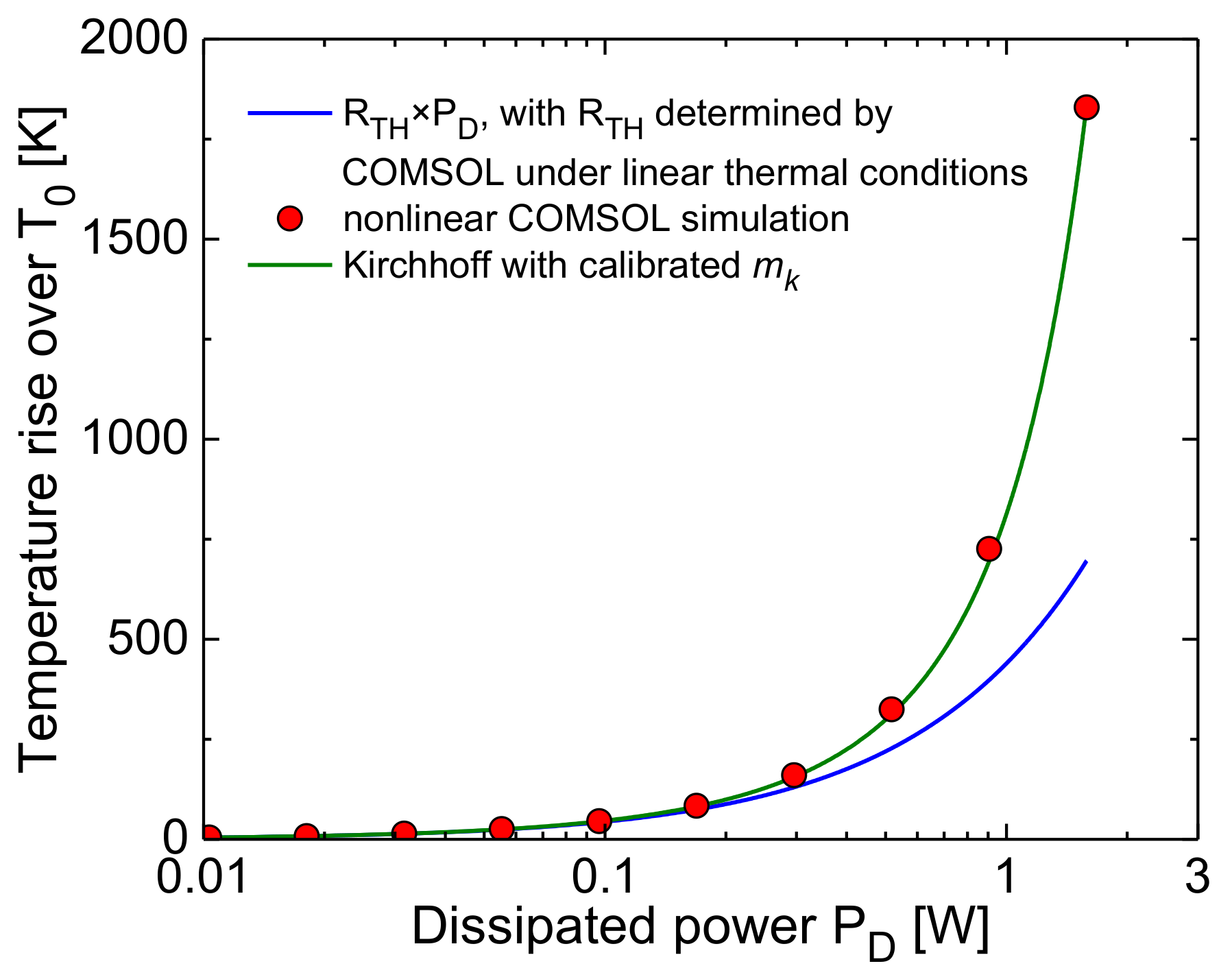
  • In [15], the Kirchhoff’s transformation was applied by assuming that all materials share the same nonlinear thermal behavior as GaAs. Unfortunately, this was found to lead to a perceptible overestimation of ET effects. Here, more realistic results are achieved by carrying out a suitable preliminary calibration procedure, similar to that made in [21].
By virtue of the above points, this work can be reviewed as an improved, and self-consistent, version of [15].
The remainder of the paper is outlined as follows. In Section 2, the technology/layout details of test devices and arrays are given. Section 3 probes into the simulation approach; in particular, the transistor model, its subcircuit representation, the COMSOL geometry/mesh generation, the FANTASTIC extraction of the RTH-based ETN, and the assembling of the final macrocircuit are described. Section 4 reports and discusses the dc ET simulation results carried out by PSPICE. Conclusions are then drawn in Section 5.

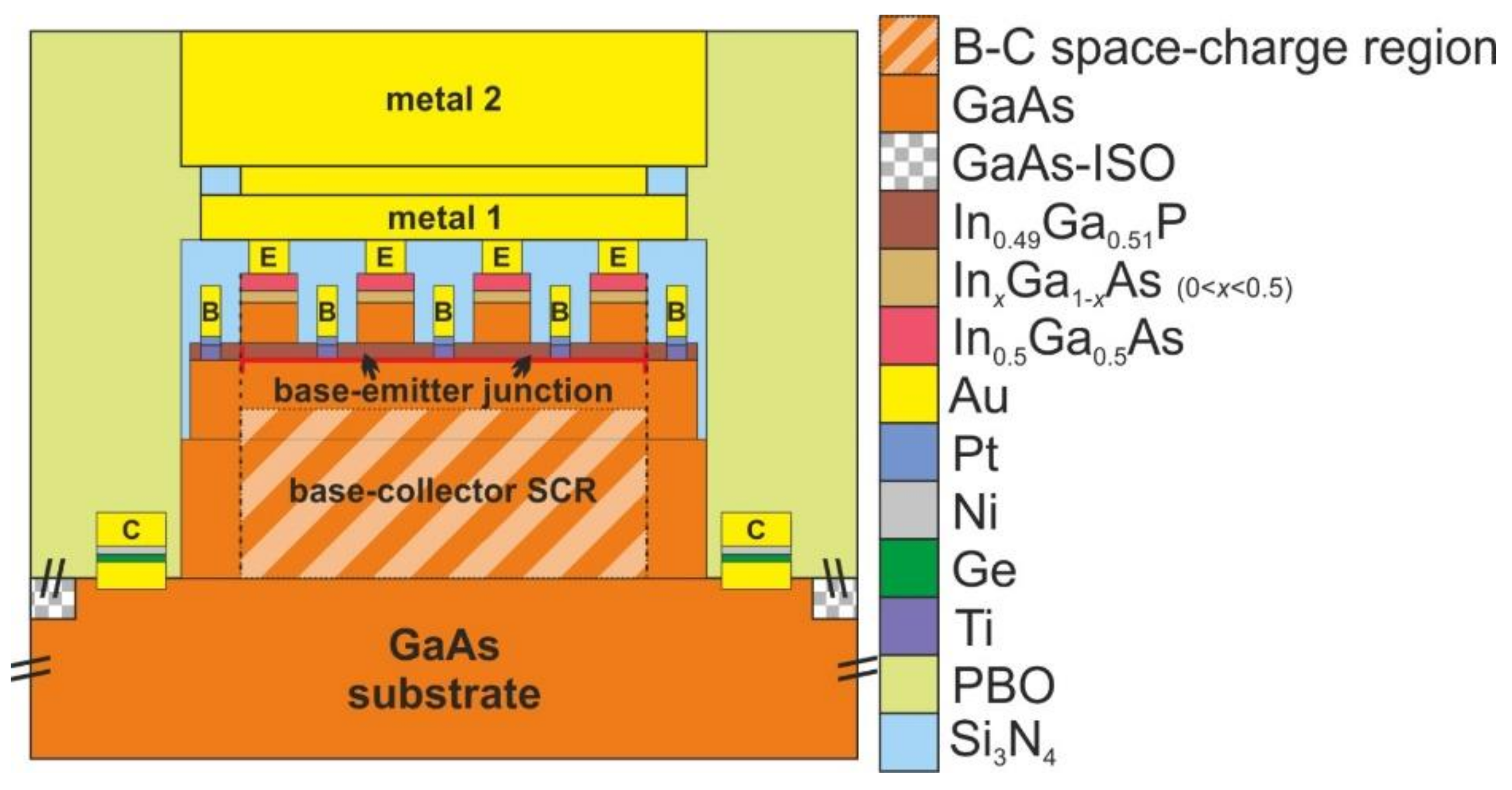
2. Devices and Arrays

The structures investigated in this paper are mesa-isolated InGaP/GaAs NPN HBTs manufactured by Qorvo using an HBT-only process (referred to as HBT8) with two metal layers (e.g., [23,24]), the key features of which are reported in Table 1. The individual transistor, hereinafter also denoted as unit cell (Figure 1), is composed by four emitter fingers, each with a 2 × 20.5 µm2 area (the total emitter area is then equal to 164 µm2). The emitter is composed by a stack of four layers, namely (from the top):
  • an In0.5Ga0.5As cap to reduce the contact resistance with the gold (Au)-based emitter metallization;
  • a grading InxGa1-xAs layer (with x spanning from 0.5 to 0) used to ensure a good lattice continuity with the underneath layer;
  • a GaAs layer acting as a set-back for an easier manufacturing process;
  • an n-doped In0.49Ga0.51P emitter layer, the bottom surface of which corresponds to the metallurgical base-emitter junction.
The base is a thin p-doped GaAs layer lying on a thick n-type GaAs mesa.
Both the base and collector contacts are designed with materials compatible with the manufacturing process in order to reduce the parasitic resistances. More specifically, the base contact is composed by the series of titanium (Ti) and platinum (Pt) layers that alloy through the leftover InGaP emitter on the base mesa, while the collector contact is located at the bottom of this mesa on the highly-doped GaAs subcollector layer and consists of a stack of Au-germanium (Ge)-nickel (Ni) layers. A metallization with two Au levels is exploited to electrically connect the unit cells and plays a role in the thermal exchange by favoring heat shunt and spread [24].
The electrical isolation from potential neighboring components is ensured by ion-implant damage (referred to as GaAs-ISO) resulting in an amorphous GaAs layer. Far from the active regions, the metal layers are separated from the GaAs substrate through a thin silicon nitride (Si3N4) layer providing some shunt effect. A 10-µm-thick polybenzoxazole (PBO) layer covers the whole structure.
The analysis first focuses on devices fabricated on a 620-µm-thick GaAs substrate (thickness normally used for testing) and provided with 65 × 65 µm2 pads (in a ground–signal–ground configuration) for bare-die experimental characterization through RF probes. The devices have been designed with a single unit cell, as well as with two and three paralleled cells, respectively (Figure 2, top). In the analysis reported in Section 4, the temperature T0 = 300 K (hereinafter also denoted as reference temperature) is assumed to be applied to the substrate backside, which can be practically done with a thermochuck.
Subsequently, the investigation is conducted on transistor arrays for PA output stages, where the unit cells are arranged in columns to (i) ensure an almost uniform distance from them to the through-wafer via providing the ground; (ii) meet the very stringent die size requirements. The arrays are assumed to be operating in a typical phone-board environment. Architectures with even and odd number of unit cells per column are examined to offer helpful guidelines to designers. In particular, arrays comprising 24 and 28 unit cells are considered, which are both arranged in four columns composed by six and seven cells each, respectively (Figure 2, bottom). In contrast to the simplified analysis performed in [15], (i) the arrays lie on a 100 µm-thick die, obtained by thinning the original 620-µm-thick wafer; (ii) the die is attached with epoxy to an 830 × 830 µm2-wide and 270 µm-thick laminate, which includes eight 600 × 600 µm2-wide 12 µm-thick Cu plates connected by nine circular Cu vias, all embedded in a dielectric; (iii) as previously mentioned, the laminate bottom is held at TB = 358 K, which is typical in the phone-board environment.

3. Simulation Approach

3.1. General Description

Similar to our previous papers [5,6,7,8,9,10,11,12,13,14,15,21], we chose to employ a circuit-based approach, which provides a good trade-off between computational overhead and accuracy. Such an approach makes use of the TEOL and can be summarized as follows:
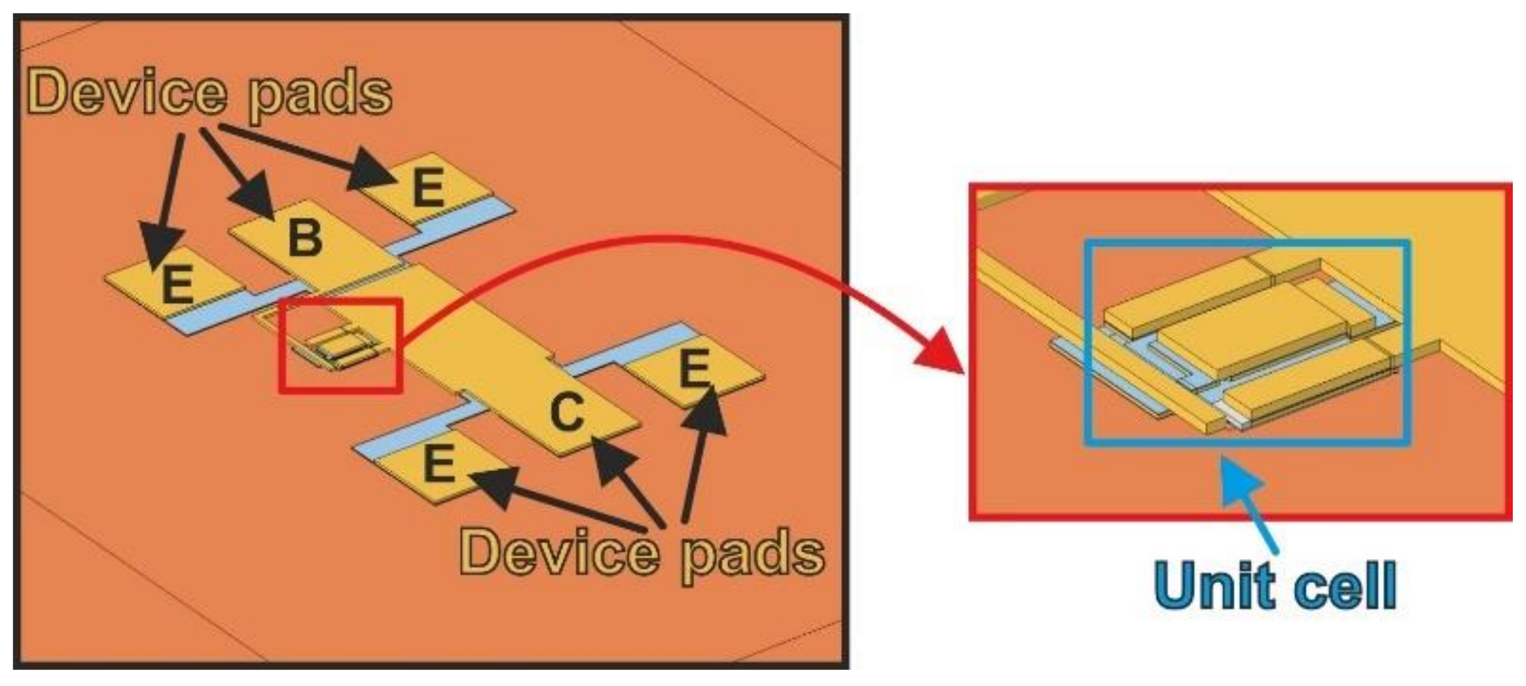
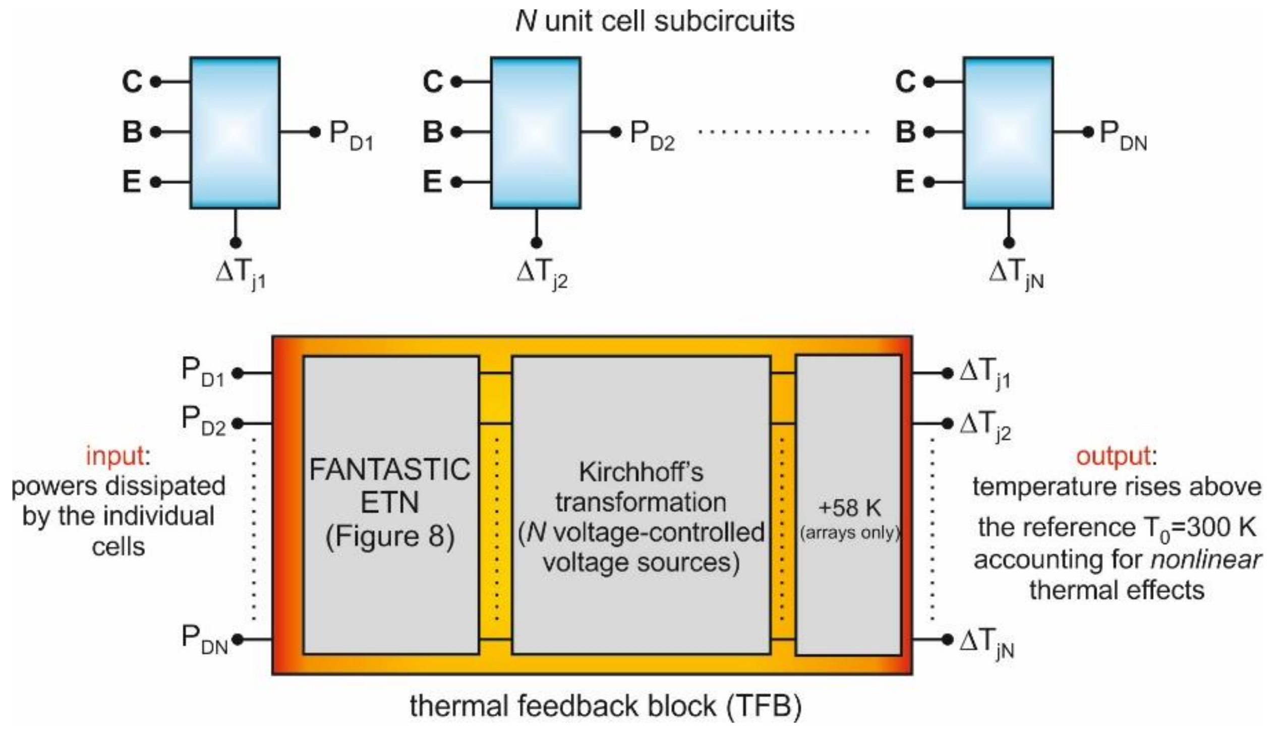
  • Each four-finger unit cell is represented with one SPICE-compatible subcircuit (Section 3.3) implementing a simple analytical transistor model (Section 3.2). This assumption relies on the following considerations: (i) the two metals uniformly distribute the temperature over the base-emitter junction; (ii) the electron currents emerging from the four closely-spaced individual emitters are expected to spread and give rise to only one heat source. The subcircuit uses (i) a basic/standard bipolar transistor at reference (and unchangeable) temperature T0 as a core component, and (ii) linear and nonlinear controlled sources to account for the variation of the temperature-sensitive parameters during the simulation run, as well as for other specific mechanisms. According to the TEOL, the temperature rise ΔTj = TjT0 averaged over the base-emitter junction (which mainly influences the ET device behavior) is actually a voltage, while the dissipated power PD is treated as a current. In addition to the standard transistor terminals (emitter, base, and collector), the unit-cell subcircuit is also equipped with an input node carrying the “voltage” ΔTj and with an output node offering the “current” PD.
  • The power-temperature feedback is described with a SPICE-compatible thermal feedback block (TFB), the construction of which is carried out in a pre-processing stage. The TFB contains an ETN including the matrix of self-heating (SH) RTHs of the unit cells and mutual RTHs among them. The inputs of the ETN are the powers PD dissipated by the cells (represented with currents), and the outputs are their temperature rises ΔTjlin = TjlinT0 for the test devices or ΔTjlinB = TjlinTB for the arrays (all emulated with voltages) under linear thermal conditions.
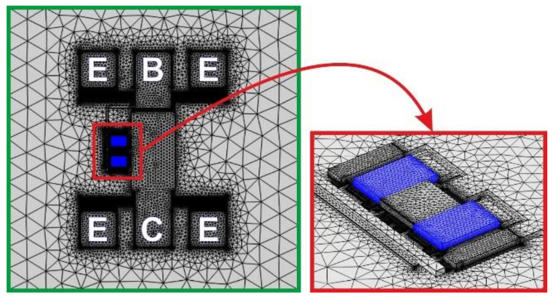
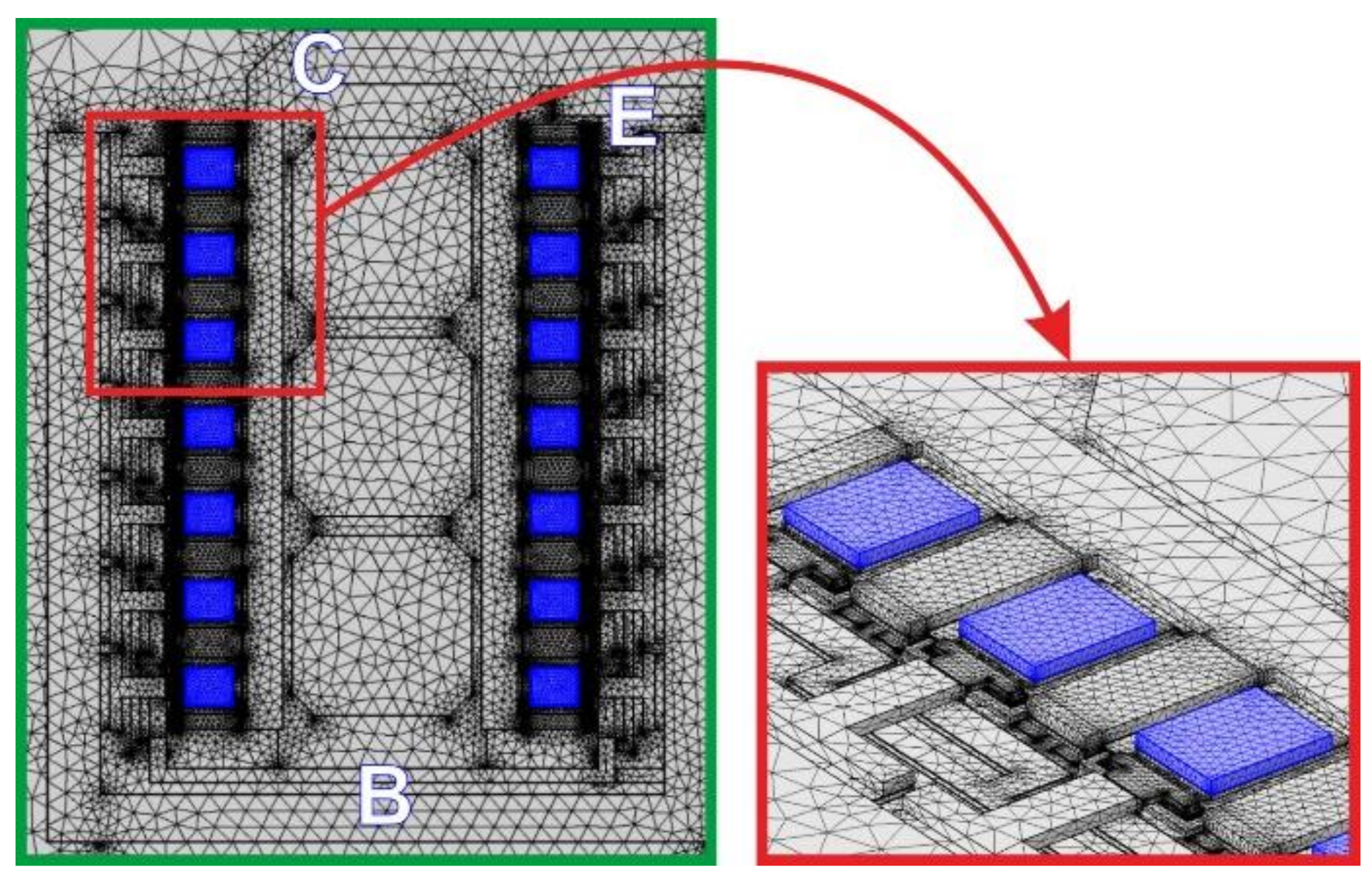
  • The ETN is automatically determined through the following procedure. First, an accurate 3-D geometry/mesh of the domain is built in the COMSOL environment using an in-house routine; then, the geometry/mesh, along with additional information concerning position/shape of heat sources, boundary conditions, and thermal conductivities, is fed to FANTASTIC, which extracts the ETN in a really short time without the need of user’s intervention/expertise or onerous FEM simulations (Section 3.5). Generally, the whole process is very fast and error-free. The adoption of FANTASTIC is an improvement over our prior contribution [15], where (i) the RTH matrix was calculated by performing N purely-thermal static COMSOL simulations by activating only one heat source at a time, and (ii) the simple ETN adopted did not allow a post-processing reconstruction of the whole temperature map in the domain.
  • As mentioned above, the ETN only accounts for linear thermal conditions. However, nonlinear thermal effects can be significant when particularly high temperatures are reached. Such effects are taken into account by making use of the Kirchhoff’s transformation, which converts the linear temperature rises ΔTjlin (test devices) or ΔTjlinB (arrays) offered by the ETN into the nonlinear counterparts ΔTj = TjT0 and ΔTjB = TjTB, respectively. Contrary to [15], here the transformation was properly calibrated (Section 3.4) to improve the ET simulation accuracy.
  • Besides the ETN, the TFB also includes N voltage-controlled voltage sources that apply the calibrated Kirchhoff’s transformation to the ETN linear outcomes; as a result, the nonlinear temperature rises ΔTj (test devices) and ΔTjB (arrays) are computed; only for the arrays, the increment TBT0 is added to ΔTjB to get the N nonlinear ΔTj = TjT0 to be provided to the unit-cell subcircuits.
  • The subcircuits are then connected to the TFB in the environment of a commercial circuit simulation tool. As a result, the whole domain is transformed into a purely-electrical macrocircuit, which inherently accounts for ET effects (Section 3.6): the temperature, and thus the temperature-sensitive parameters, are allowed to vary during the simulation run. The task of solving this macrocircuit is given to the powerful and robust engine of the circuit simulation tool, with very low computational effort and minimized occurrence of convergence issues compared to other numerical methods.

3.2. Bipolar Transistor Model

The analytical model used to describe the dc behavior of the unit cell is simple, accurate enough, and associated to a low-effort parameter extraction process; this provides high flexibility to the overall approach. The collector current in forward active mode is given by [13]
I C = I C n o A V + I A V = M · I C n o A V = M · 1 + V C B V A F · 1 B H I · A E · J S 0 · exp V B E j + ϕ · Δ T j η · V T 0
where:
  • ICnoAV [A] is the collector current in the absence of impact-ionization (II), or avalanche, effects;
  • IAV [A] is the collector current component only induced by avalanche;
  • VCB [V] is the collector-base voltage;
  • VAF [V] is the forward Early voltage;
  • M (≥ 1) is the dimensionless VCB-dependent avalanche multiplication factor;
  • AE [µm2] is the emitter area;
  • JS0 [A/µm2] is the reverse saturation current density at the reference temperature T0 = 300 K;
  • η is the ideality coefficient at T0;
  • VT0 = 0.02586 V is the thermal voltage at T0;
  • VBEj [V] is the internal (junction) base-emitter voltage, that is, VBEj = VBERB·IBRE·IE, where VBE is the externally-accessible base-emitter voltage, IB, IE [A] are the base and emitter currents, and RB, RE [Ω] are the parasitic base and emitter resistances, respectively;
  • the temperature rise ΔTj [K] is defined as TjT0, Tj being the temperature averaged over the base-emitter junction;
  • ϕ [V/K] is the temperature coefficient of VBEj;
  • BHI (≥1) is an IE-dependent dimensionless term introduced to describe the attenuation dictated by high-injection (HI) effects, i.e., the Kirk-induced gain roll-off.
In this approach, the temperature dependence of IC is taken into account with a VBEj shift, while JS0, η, and VT0 are kept at their T0 values (e.g., [25]). Coefficient ϕ [V/K] is assumed to vary with emitter current IE according to the following logarithmic law [11,13,26,27,28,29]:
ϕ = ϕ 0 η · k q · ln I E A E · J S 0
where k [eV/K] is the Boltzmann’s constant, and q [C] is the (absolute value of the) electron charge; parameter ϕ0 can be extracted by comparing (1) with ICVBE characteristics measured at various backside temperatures at low current levels for VCB = 0 V [29].
As far as factor M is concerned, any model can in principle be adopted. For the GaAs HBTs under analysis, we chose the classic Miller model given by [30]
M = 1 1 V C B B V C B O n A V
BVCBO [V] and nAV being the open-emitter breakdown voltage and a fitting power factor, respectively.
The HI attenuation term BHI is modeled as [5,13]
B H I = 1 + α F · I E A E · J H I n H I
where αF is the common-base (CB) forward current gain, while JHI [A/µm2] and nHI are fitting parameters.
The common-emitter (CE) forward current gain βF is modeled as
β F = β F 0 · 1 + V C B V A F · 1 B H I · exp Δ E G k · 1 Δ T j + T 0 1 T 0
where βF0 is the gain at T0, at medium current levels (i.e., before the Kirk-induced fall-off), and in the absence of Early effect, while ΔEG [eV] is the positive difference between the bandgaps of emitter and base yielding a negative temperature coefficient (NTC). The CB gain αF in (4) is related to the CE counterpart by αF = βF/(1 + βF).
The base current is given by (e.g., [13,31])
I B = I B n o A V I A V = I C n o A V β F M 1 · I C n o A V = I C n o A V · 1 α F M = I C · 1 α F M 1
where use has been made of (1).
We note that replacing the simple M formulation (3) with a more complex one (e.g., [31]), the model can be adopted for bipolar transistors fabricated in any technology if a proper parameter calibration procedure is performed (in silicon devices, ΔEG is negative, since the emitter bandgap is narrower than that of the base due to high doping levels).
The parameter extraction procedure is straightforward (details are reported in [29]). The values adopted for the simulations described in Section 4 are reported in Table 2.

3.3. SPICE Unit-Cell Subcircuit

A sketch of the subcircuit is reported in Figure 3, which evidences the standard bipolar transistor model as a core component at temperature T0, as well as the additional ΔTj (input) and PD (output) terminals. Linear/nonlinear controlled voltage/current sources are added to enable the variation of the temperature-sensitive parameters during the simulation run, as well as to account for physical mechanisms not included in the standard transistor (for this reason, the resulting subcircuit is also popularly referred to as wrapper model). The II-free collector current ICnoAV accounting for the temperature dependence of VBEj, HI, and Early effects is computed with the nonlinear source denoted with A. The II-unaffected base current IBnoAV is calculated by source B as ICnoAVF, βF being evaluated by the nonlinear source C from VCB, IE, and ΔTj according to (5). The II (avalanche) current IAV is determined as (M − 1) × ICnoAV by source D, where factor M described by (3) is provided by the nonlinear source E; the collector current IC is obtained by adding IAV to ICnoAV, while the base current IB is given by IBnoAV-IAV. The lumped resistances RB and RE emulate the parasitic base and emitter resistances, respectively. The subcircuit also includes further nonlinear sources (omitted in Figure 3) to describe the cell behavior in saturation mode. The dissipated power PD under dc conditions (to be given to the TFB) is determined as
P D = I B · V B E + I C · V C E = I E · V B E + I C · V C B

3.4. Construction of the Geometry/Mesh in COMSOL and Calibration of the Kirchhoff’s Transformation

The 3-D geometry/mesh of each domain was constructed in the environment of the COMSOL software package [16] by making use of an in-house routine that relies on the MATLAB-COMSOL Livelink and the Toolbox for files in GDSII format provided by U. Griesmann [17]. The procedure is described as follows: first, the GDS layout file (i.e., the masks used for the technological process) is input to the routine along with the thicknesses of the layers, mask biases, and material parameters; then, the routine automatically draws the 3-D geometry, and finally generates and optimizes the mesh in the COMSOL environment. Such a process is error-free and requires a much shorter time compared to a painstakingly-long manual approach.
A single heat source (geometrically coinciding with the base-collector SCR [17]) and a single subcircuit were assigned to each unit cell (Figure 1); as mentioned earlier (Section 3.1), this intrinsically assumes that the fingers within the cell are tightly thermally coupled, and thus not prone to thermal hogging. Figure 4 depicts the geometry of the 1-cell test device, while Figure 5 shows the mesh of the 2-cell one.
For the arrays, the horizontal symmetry was exploited to construct the geometry/mesh of only half of the domains (Figure 2, bottom), thus alleviating the computational burden; the missing portions were virtually restored by applying an adiabatic boundary condition to the plane of symmetry. Figure 6 illustrates the geometry of (half of) the 24-cell array, while Figure 7 shows the mesh of (half of) the 28-cell array, both in COMSOL.
Besides the geometry/mesh of the domains and the position of the heat sources, FANTASTIC [22,23] requires information on the boundary conditions and thermal conductivities to extract the ETN including the RTH matrix (Section 3.5). As mentioned in Section 2, the backside of the GaAs substrate was assumed to be at T0 for the test devices, while the laminate bottom was set to TB for the arrays. All the other surfaces were considered adiabatic (i.e., with zero outgoing heat flux), such an assumption being justified by the particular scratch-protection coating employed in the technology (thick PBO).
The thermal conductivities associated to the materials of the test devices (at T0) and arrays (at TB) are listed in Table 3.
The ETN is generated by FANTASTIC under linear thermal conditions (temperature-insensitive thermal conductivities). However, as very high temperatures are reached, nonlinear thermal effects can no longer be neglected. More specifically, the thermal conductivities of the materials vary with temperature T according to the following laws:
k T = k T 0 · T T 0 α
k T = k T 0 β · T T 0
where (8) applies to semiconductors and insulators, and (9) to some metals; the accepted values of the α and β coefficients are also reported in Table 3. In order to account for the temperature dependences described by (8) and (9), we resorted to the Kirchhoff’s transformation [18,19], which converts the linear junction temperature rises (ΔTjlin and ΔTjlinB) into the nonlinear counterparts (ΔTj and ΔTjB) through [36]
Δ T j = T j T 0 = T 0 · m k + 1 m k · Δ T j l i n + T 0 T 0 1 1 m k T 0 = T 0 · 1 + 1 m k · Δ T j l i n T 0 1 1 m k T 0
for the test devices, and
Δ T j B = T j T B = T B · m k + 1 m k · Δ T j l i n B + T B T B 1 1 m k T B = T B · 1 + 1 m k · Δ T j l i n B T B 1 1 m k T B
for the arrays. Contrary to the simplified analysis in [15], where mk was chosen equal to 1.25 (α value for GaAs) for all the domains under investigation, here a preliminary calibration procedure was performed for this parameter. Let us refer to the 1-cell test device for the sake of simplicity. This HBT was simulated with COMSOL over a wide range of dissipated powers PD by activating the thermal conductivity dependences upon temperature (8), (9) (nonlinear thermal conditions), and the average temperature rise over T0 at the base-emitter junction ΔTj was computed for each PD. The linear temperature rise ΔTjlin over the same PD span was evaluated by multiplying PD by the RTH obtained by COMSOL under linear conditions. Then the Kirchhoff’s transformation was applied to ΔTjlin, and mk was tuned so as to ensure the best agreement between the nonlinear temperature rise ΔTj calculated by the transformation and the realistic one evaluated by COMSOL; the optimum mk value was 0.8333 (Figure 8). The same operation was repeated by activating one cell belonging to an array and considering the average junction temperature rise over TB; in that case, the optimum mk value was found to be 0.8932. As a result, mk = 0.8333 was used in (10) for the ET simulations of the test devices (Section 4.1), whereas mk = 0.8932 was adopted in (11) for the ET simulations of the arrays (Section 4.2).

3.5. FANTASTIC

The FAst Novel Thermal Analysis Simulation Tool for Integrated Circuits (FANTASTIC), originally presented in [22,23], was conceived and developed to approximate a FEM model of heat conduction in an electronic device, having typically millions of DoFs, with a dynamic compact thermal model (DCTM), having only tens of DoFs, and the corresponding ETN [21]. The extraction of the DCTM and ETN does not require to solve the FEM model, as it is performed in short times through a refinement of the truncated balance-based moment matching approach to model-order reduction (MOR) introduced in [37]. Moreover, it also allows the extraction of a static compact thermal model (SCTM) and the related ETN relying on the RTH matrix (hereinafter indicated with RTH); for this simplified case, FANTASTIC is even quicker, as briefly discussed below.
The heat conduction problem in the structure, assumed to be static and linear, is imported from either commercial (e.g., COMSOL) or open-source numerical tools in the form of: mesh discretizing the geometry, position/shape of the heat sources, boundary conditions, and thermal conductivities (also mass densities and specific heats are required for the dynamic case). Both hexahedral and tetrahedral meshes can be used. Arbitrary tensorial thermal conductivity distributions can be defined. Neumann’s, Dirichlet’s, or Robin’s boundary conditions can be applied.
A FEM model of the problem is then assembled by FANTASTIC. In particular, the stiffness matrix K is constructed. High-order basis functions can be adopted; the typical choice is to select tetrahedral meshes and 2nd-order basis functions, as a good trade-off between accuracy and efficiency. The M DoFs of the temperature rise distribution, forming the M-row vector ϑ, are solution of the discretized heat conduction problem
K ϑ = q
in which the power density distribution vector q takes the form
q = Q P D
In (13), PD is an N-row vector with the powers dissipated by the N heat sources, and Q is an M × N matrix, the n-th column of which is the power density distribution vector of the n-th heat source, with n = 1, …, N. The port temperature rises of the N heat sources form the N-row column vector ΔTjlinTjlinB for the arrays) defined as [37]
Δ T j l i n = Q T ϑ
In order to extract a compact thermal model, an M × M ^ matrix V with M ^ M is defined, which allows expressing ϑ by means of a reduced number M ^ of DoFs, thus forming the M ^ -vector ϑ ^ so that
ϑ = V ϑ ^
The V matrix is used for projecting the discretized heat conduction problem (12)–(14) by the Galerkin’s method, deriving an SCTM in the form
K ^ ϑ ^ = q ^
where
q ^ = G ^ P D
Δ T j l i n = G ^ T ϑ
in which
K ^ = V T K V
is an M ^ th-order matrix and
G ^ = V T Q
is an M ^ × N matrix. The V matrix is determined by the Algorithm 1 reported below.
Algorithm 1: SCTM extraction
 Set V:=0
for each heat source n=1, …, N do
1  Solve (21) for Θn
2  Update matrix V by appending Θn
3  Generate a SCTM projecting (12)–(14) onto V
At line 1, the temperature response to the n-th heat source is solved for the static heat conduction problem. Thus, equation
K Θ n = Q e n
is solved for Θn, en being the vector selecting the n-th column of Q. Since the coefficient matrices of these linear systems are symmetric positive definite, the most efficient multigrid iterative solvers can be used for their solution.
At line 2, the V matrix is updated by appending vector Θn to its columns if it is linearly independent with respect to them.
At line 3, the SCTM is determined proceeding as in (16)–(18), and has dimension M ^ NM. A much smaller dimension is thus obtained with respect to the dynamic case; moreover, since a much smaller number of discretized heat conduction problems are solved, a large speedup of the algorithm is also achieved.
It is now observed that by solving at limited cost the eigenvalue problem
U ^ T K ^ U ^ = Λ ^
having as unknown the M ^ th-order orthogonal matrix U ^ , in which Λ ^ is an M ^ th-order diagonal matrix, and introducing the change of variables
ϑ ^ = U ^ ξ ^
the SCTM Equations (16)–(18) are transformed into the equivalent form
Λ ^ ξ ^ = Γ ^ P D
Δ T j l i n = Γ ^ T ξ ^
where Γ ^ is the M ^ × N matrix V ^ T G ^ . The spatial distribution of the temperature rise is then reconstructed as
ϑ = Ξ ξ ^
Being Ξ = V U ^ an M × M ^ matrix like V. The ξ ^ vector encompasses the DoFs of the thermal field. These DoFs are the node temperature rises in the extracted ETN sketched in Figure 9, which is governed by (24) and (25) and represents a simplified version of the dynamic counterpart [21,22,23], as it benefits from a much lower (by one order of magnitude) number of nodes, resistances, and controlled sources. The ETN transforms the port powers PD into the port temperature rises ΔTjlin by inherently accounting for the boundary conditions initially applied to the FEM model. The port response of this network defines the Nth-order resistance matrix R ^ TH [K/W] of the SCTM given by Q ^ T K ^ 1 Q ^ . Since by construction the M ^ columns of the V matrix span the N columns of matrix K−1Q, it is straightforward to prove that R ^ TH = RTH, where RTH is the thermal resistance matrix of the discretized heat conduction problem (12)–(14) given by QTK−1Q. This further strengthens the general result relating the thermal impedance matrices of the compact thermal model and of the discretized heat conduction problem in the dynamic case [38].
The resulting ETN is particularly well-suited to be solved by means of modified nodal analysis in SPICE-like circuit simulators, since all circuit elements are voltage-controlled, and thus the number of variables added by the SCTM is limited to M ^ . The topology is general and can be implemented into any circuit simulation program.
It is worth noting that, after the circuit simulation, as a post-processing stage, the whole spatial distribution of temperature rise in the examined domain can be reconstructed at negligible computational cost and memory storage using (26), for both thermal-only and ET simulations. The temperature map can be plotted by any proper tool, like e.g., Paraview. This option is not allowed using conventional ETNs like in our former paper [15].

3.6. Construction of the Macrocircuit

The ETN derived by FANTASTIC was enriched with N nonlinear voltage-controlled voltage sources to account for the Kirchhoff’s transformation, and the TFB was then obtained. The ΔTj and PD nodes of the subcircuits (the unit cells) were connected to the TFB, thereby giving rise to the whole TEOL-based SPICE-compatible macrocircuit, a simplified scheme of which is reported in Figure 10. As previously mentioned, the solution of the macrocircuit was delegated to PSPICE [20], although any other commercial circuit simulation software (e.g., LTSPICE, Eldo, Keysight ADS [39], and SIMetrix) could in principle be used.

3.7. Extension to the Dynamic Case

Unlike advanced bipolar transistor models equipped with temperature-dependent parameters and a thermal node (like HiCUM [40], VBIC, AHBT, and Mextram504, all available in ADS), the proposed unit-cell model/subcircuit is only suited to fairly well describe forward active and saturation modes under dc conditions. RF simulations including ET effects can be enabled by resorting to a variant of our approach based on one of the above models in the ADS environment; the strategy can be described as follows.
  • The selected transistor model must be provided with a power (output) node, and the internal one- or two-pair thermal network has to be deactivated.
  • All parameters of the model must be extracted from experimental data, which is a nontrivial task.
  • As mentioned in Section 3.5, if FANTASTIC is also fed with the mass density and specific heat for all materials, it can be enabled to extract a DCTM of the domain and the associated ETN accounting for the dynamic heat propagation [21,22,23]. Such an ETN, together with the Kirchhoff’s transformation sources, will constitute the SPICE- and ADS-compatible TFB.
  • Lastly, the macrocircuit has to be built in ADS by connecting the model instances among them and with the TFB.
It is worth noting that the adoption of the one- or two-pair thermal networks embedded in the transistor models instead of our TFB (i) would lead to a significant inaccuracy in terms of SH of the single cell (the typically-used single pair is not enough for the transient SH response [23]), and (ii) would exclude the mutual thermal interactions among unit cells, which however play a relevant role, as demonstrated in Section 4.
As an alternative, one could resort to an ET solver available in recent ADS releases, which couples a quasi−3-D layout-based numerical thermal tool to the circuit simulator (the thermal networks embedded in the model instances being disabled) [41]. However, (i) this strategy is only applicable to device models equipped with a thermal node; (ii) using such a solver for layout optimization is very labor-intensive; (iii) the iterative process leading to convergence is resource-hungry.

4. Results and Discussion

4.1. Test Devices

The analysis of the test devices is two-fold: it is intended (i) to offer an overview of the ET- and II-induced positive-feedback mechanisms limiting the safe operating region, and (ii) to explore the thermally-stabilizing effect ensured by the base ballasting. In the latter case, an integrated resistor RBext = 400 Ω was used per each cell, as this is the typical ballasting strategy chosen for the arrays investigated in Section 4.2.
Let us first consider the single-cell device, which does not require an ETN, but only a linear SH RTH to which the Kirchhoff’s transformation is applied. The RTH was computed to be about 440 K/W, which is in good agreement with the experimental value extracted by means of the classic method proposed in [42]. Figure 11 shows the VBE-constant ICVCE and ΔTjVCE characteristics. It can be inferred that the curves of the unballasted device are affected by a flyback (also denoted as snapback or turnover) mechanism followed by a negative-differential-resistance (NDR) branch [6,13,31,43,44,45,46], which can be simulated/measured by (i) incrementing IC or (ii) connecting a resistor RCext to the collector terminal, sweeping VCext on the available resistor node (Cext), and evaluating VCE as VCextERCext·IC. It is worth noting that increasing VCE beyond the value corresponding to the flyback would have instead led to a thermal runaway (shown for VBE = 1.25 V) and sudden device failure. Adding a base-ballasting resistor (as suggested in [31,47,48]) with RBext = 400 Ω prevents the flyback (and thus the runaway); however, it reduces the internal (junction) VBEj at medium/high current levels, decreasing and limiting the collector current.
Figure 12 shows the behavior of the 2-cell test device under IBTOT-constant conditions. As can be seen, a bifurcation phenomenon is triggered: beyond a critical VCE, cell #2 tends to conduct the whole current, while #1 gradually turns off [26,49,50,51]. For IBTOT = 0.5 mA, the critical VCE is equal to 8 V for the unballasted case, and reduces with increasing IBTOT. It is not possible to identify a priori which cell will take all the current, since it is determined by random (and unavoidable) technology and layout fluctuations. In PSPICE the cells are assumed electrically identical, and the current hogging in cell #2 is favored by a marginally higher SH RTH due to a slight layout asymmetry. As far as the total collector current ICTOT is concerned, a smooth NDR region due to the βF NTC is observed in the VCE range where ICTOT is equally shared by the two cells. The NDR mechanism is then replaced by a marked ICTOT reduction within the bifurcation region due to the ‘faster’ temperature growth with VCE in the hotter cell, which implies a significant βF decrease; such a behavior is also denoted as collapse of collector current [49] or collapse of current gain [26,50,51]. As VCE exceeds 13 V, the II current IAV2 (≈90 µA at VCE = 15 V) can no longer be neglected with respect to IBTOT (=500 µA); as a result, the avalanche-less current IBnoAV2, almost equal to IBTOT + IAV2, perceptibly grows due to the IAV2 increase, and in turn raises ICnoAV2IC2ICTOT. The inclusion of base ballasting with RBext = 400 Ω per cell pushes the critical VCE to 16.6 V, restoring a uniform behavior over a large voltage range [47].
Figure 13 illustrates the behavior of the 2-cell test device under VBE-constant conditions. Let us first examine the unballasted case. If ICTOT is swept, the current is equally divided between the unit cells until a flyback takes place, followed by an NDR branch still showing uniform operation; at low VBE (e.g., 1.2 V), a bifurcation will also occur for relatively low cell temperatures [31]. A similar behavior was observed for more paralleled BJTs in SOG technology [7]; in that case, an uneven current distribution was found to arise beyond the uniform NDR branch under ICTOT-controlled conditions. By increasing VCE, the whole device (or at least one of the two cells) would have blown up beyond the value corresponding to the flyback; this means that our simulations do not confirm the observation of a ‘safe’ collapse encountered in [50,51].
Let us next consider the device with base-ballasted cells subject to the same biasing conditions (Figure 14). As far as the VBE = 1.2 V case is concerned, the flyback point moves to the left, thus shrinking the VCE-controlled safe operating region; this can be ascribed to the increased avalanche current flowing in the unit cells, in turn induced by RBext = 400 Ω, which favors the positive feedback action related to II [31,48]. On the other hand, the thermally-induced bifurcation disappears; it was found than the bifurcation-triggered discrepancy between IC1 and IC2 reduces with increasing RBext, and RBext = 400 Ω is the threshold value for which the uniform behavior is fully restored. For higher VBEs, the ballasting makes the flyback mechanism vanish, thus improving the thermal stability of the device; however, the current capability significantly plummets at high current levels.
It is also important to analyze the ET behavior of the 2-cell device under IETOT-controlled conditions, typical for differential pairs and comparators [52,53]. Results obtained by increasing the total emitter current IETOT for VCB = 8 V are shown in Figure 15 for both the unballasted and ballasted cases. It is shown that without ballasting a bifurcation phenomenon is triggered for a critical IETOT (33 mA), and the whole ICTOT eventually flows in cell #2, rapidly increasing its temperature; a similar behavior would be obtained by fixing IETOT and sweeping VCB [6,31]. Applying the resistors RBext = 400 Ω, thermal effects are weakened and the bifurcation disappears, limiting the maximum temperature reached by the device.
We now consider the ET behavior of the test device composed by three unit cells, assumed ideally identical in PSPICE. The first simulation was performed under CE conditions by increasing VCE with a constant IBTOT = 0.7 mA (Figure 16). Let us focus on the unballasted case. It is found that cell #2 starts conducting more current due to the thermal coupling with both the adjacent (outer) cells #1 and #3. For higher VCE values, a counterintuitive behavior takes place: a bifurcation mechanism involving cells #1 and #3 occurs at VCE = 7 V; in particular, cell #3 eventually bears more current, whereas #1 turns off, as induced by the slightly higher SH RTH of #3 with respect to #1. By further increasing VCE, cell #3 prevails over #2 since the SH RTH of #3 (396.2 K/W under linear thermal conditions) is perceptibly higher than that of cell #2 (361.7 K/W), which experiences a more effective heat flow through metal 2 (top metal). The strongly uneven current distribution for VCE > 7 V turns into a collapse in the ICTOTVCE curve. For VCE > 13 V, cell #3 conducts the whole current, and therefore IB3 = IBnoAV3IAV3 is almost equal to IBTOT = 0.7 mA; the increase in IAV3 with VCE due to the enhanced II leads to a growth in IBnoAV3, which dominates over the NTC of βF3, thus driving an IC3ICTOT increase. Adopting RBext = 400 Ω for all cells pushes the uneven current distribution to VCE > 15.7 V, thus leading to a much wider uniform operating region.
It is worth noting that increasing the emitter area of cell #1 by only 1 µm2, the onset of the bifurcation takes place at the same critical VCE, but the behavior of cells #1 and #3 reverses: cell #1 prevails over #3, and eventually sinks also the current of #2. Nevertheless, the ICTOTVCE curve would coincide with that obtained for cells sharing ideally identical areas. This means that it is impossible to foresee which of the outer cells will dominate, since it depends on unavoidable technological/layout discrepancies. The practical implication is that the failure analysis should look at planes of symmetry, and not at the specific failed cells.
An overview of the ICTOTVCE characteristics for various IBTOT values is illustrated in Figure 17 for both the unballasted and base-ballasted cases; it is apparent how the collapse locus (which can be reviewed as the boundary of the safe operating area) significantly moves rightward by virtue of the external base resistances [47].
In the above analysis, it was stated that the 3-cell test device benefits from a lower SH RTH of the inner cell #2 compared to the outer cells. We decided to quantify the related thermally-stabilizing effect by performing a test simulation where the RTH of cell #2 was considered identical to those of the lateral cells (396 K/W under linear thermal conditions) and the mutual RTHs between adjacent cells were assumed to coincide (115 K/W). Figure 18 shows that the classic collapse with #2 conducting the whole current is obtained. Unfortunately, the collapse onset in the ICTOTVCE characteristic takes place at the same VCE as in the real test device with lower RTH for cell #2; this means that the bifurcation mechanism occurring for the outer cells in the real case is as deleterious as the strong thermal coupling affecting #2 in the ideal device with uniform SH RTHs.

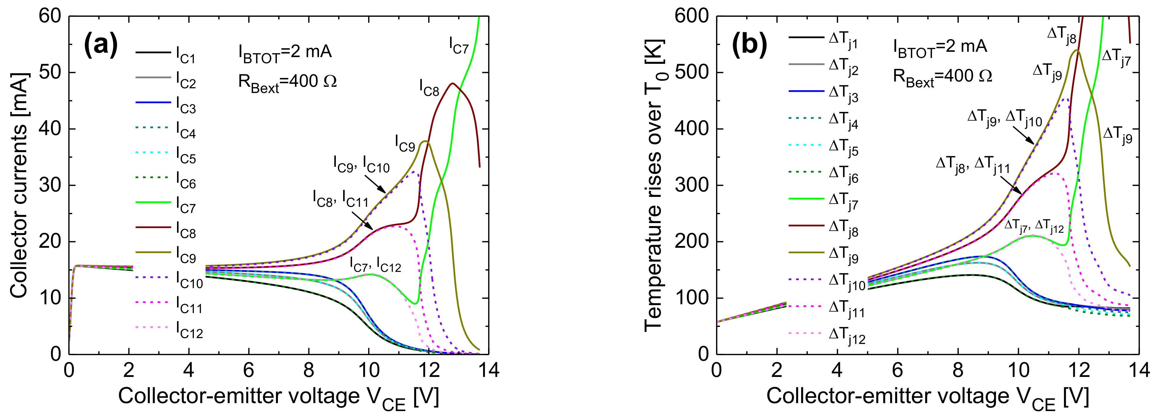
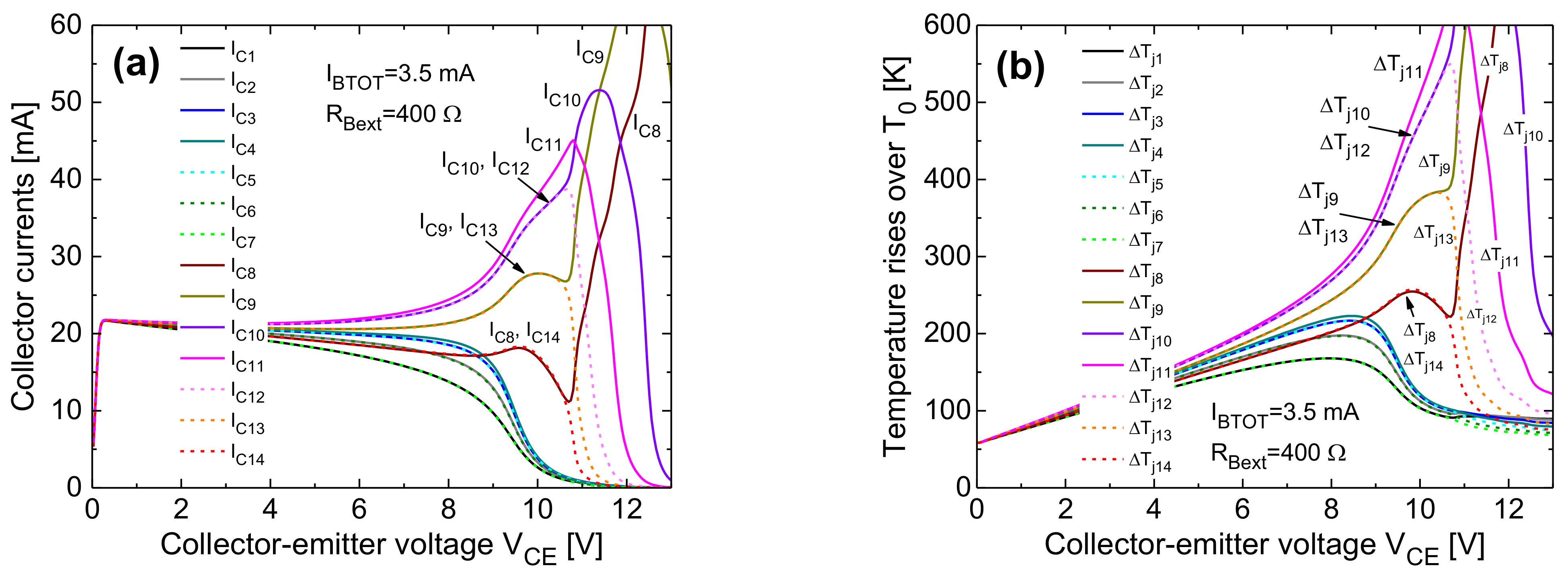
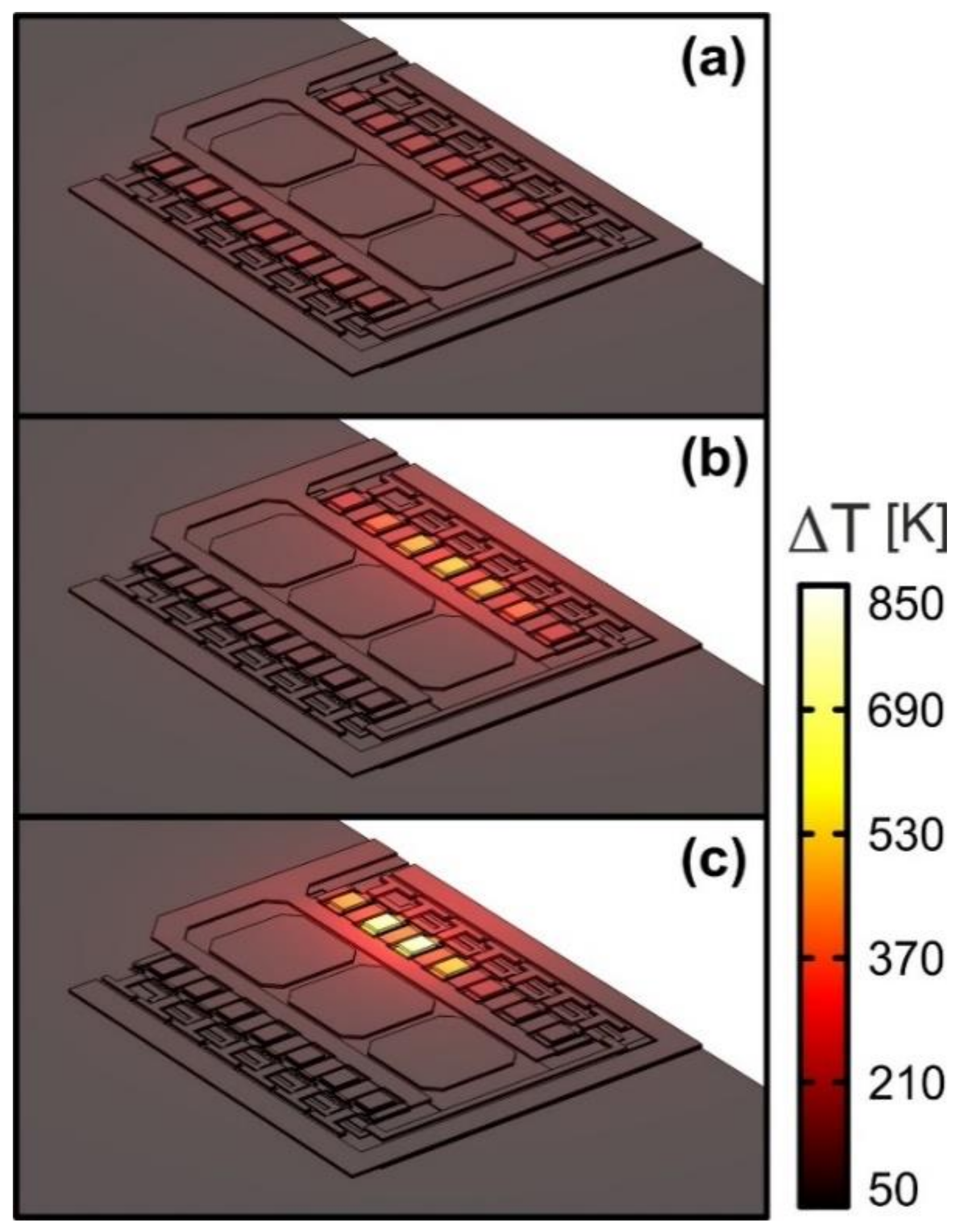
4.2. Transistor Arrays

As already mentioned in Section 2 and Section 3.4, only half of each array for PA output stages was drawn, meshed, and simulated by exploiting the horizontal symmetry. This means that only 12 (14) cells were taken into account for the 24-cell (28-cell) arrays. Our simulation approach allows monitoring the dc ET behavior of the arrays at cell-level, that is, besides the junction temperature, all the key parameters, voltages, and currents are available for each cell; this would have been unviable by performing experiments since the collector layers of the individual cells are all shorted to one another, by being in a single isolation tub.
Hereinafter, ICTOT and IBTOT are the total collector and base currents of the semi-arrays.
The analysis focuses on IBTOT-constant CE conditions, since GSM PAs are more or less biased with a constant IBTOT. A base ballasting with the nominal value RBext = 400 Ω per unit cell was applied following a strategy denoted as segmented or split, in which such resistances only appear in the dc path and there is no RF performance penalty. The bottom of the laminate was held at TB.
Let us first consider the halved 24-cell array. Figure 19 reports the PSPICE results corresponding to IBTOT = 2 mA; the simulation lasted less than 100 s on a normal PC, in spite of the very small VCE step used. A significant current/temperature nonuniformity is observed as VCE exceeds 9 V, leading to an ICTOT collapse; more specifically, the right (internal) column (#7 to #12) conducts the entire current, while the cells belonging to the left (external) one (#1 to #6) tend to turn off. Below VCE = 11 V, the symmetric cell pairs of the right column (namely, #9 and #10, #8 and #11, and #7 and #12) share the same current. For VCE higher than 11 V, a bifurcation mechanism occurs for all these pairs, as dictated by slight layout asymmetries: in particular, the top cells (#7, #8, and #9) prevail over the bottom counterparts (#10, #11, and #12, respectively). The uneven behavior is thus enhanced, and ICTOT decreases more steeply with VCE. Over the VCE span from 11 to 12 V, cell #9 is the hottest cell since it suffers from the stronger thermal coupling with the surrounding cells. As VCE exceeds 12 V, only the adjacent cells #7 to #9 are conducting, whereas cells #10 to #12 run dry; as a consequence, mutual thermal interactions among cells play a minor role, while the behavior is dominated by the SH RTHs of the "active" cells, namely, 541, 533.3, and 531.5 K/W for #7, #8, and #9, respectively, under linear conditions (the closer the cell to the die border, the higher the RTH). For a higher VCE, the total current first focuses over cells #7 and #8 (at VCE = 12.6 V, ΔTj7 = 500 K, and ΔTj8 = 700 K), and then, if #8 survives, over cell #7 only.
It must be remarked that introducing an intentional (very small) technological discrepancy between #9 and #10 to favor a slightly higher conduction of #10, for VCE > 11 V the bottom cells of the right column dominate over the top ones; by further increasing VCE, cells #11 and #12 sink the whole current, which eventually focuses in the outer #12 suffering from the highest RTH. The ICTOTVCE curve, including the collapse region, remains instead unaltered.
If the applied IBTOT is higher, the current nonuniformity (i.e., the collapse onset) and the subsequent bifurcation phenomenon involving symmetric cells occur for slightly lower critical VCEs, as ET effects are exacerbated by the higher currents (and dissipated powers). Clearly, the temperatures reached by the right-column cells at the bifurcation are higher than in the lower-IBTOT case. Figure 20 illustrates the scenario corresponding to IBTOT = 3 mA; here it is shown that, as the bifurcation takes place, the ΔTj shared by the inner cells #9 and #10 has already exceeded 600 K; this suggests that in a real array the metallization and surrounding interlevel dielectrics of these cells is likely to melt before the bifurcation arises.
In the total absence of ballasting, the VCE range enjoying uniform current and temperature distribution dramatically reduces; beyond a critical (and low) VCE, the pair #9, #10 starts taking more current, which translates in the collapse onset in the ICTOTVCE characteristic; then, the bifurcation between symmetric cells in the right column arises, and, for a slightly higher VCE, the current flows only in cell #9. An example is reported in Figure 21, which corresponds to IBTOT = 3 mA. It is observed that, as #9 dominates, the cells symmetric with respect to #9 (i.e., #8 and #10, and #7 and #11) tend to exhibit a similar behavior (i.e., they conduct almost the same current and are at the same temperature). Again, by intentionally applying a technological discrepancy leading to a slightly higher current capability for cell #10, the current will focus only on this cell in the deep collapse region, without distorting the ICTOTVCE characteristic.
Finally, the case of emitter ballasting with REext = 4 Ω per cell is examined, as it is considered approximately equivalent to RBext = 400 Ω by circuit designers; however, in this case a significant degradation in terms of fT and fMAX (both by some GHz), as well as of RF gain, is induced. Figure 22 depicts the individual collector currents of the unit cells and the associated temperature rises above T0 with IBTOT = 3 mA applied. By virtue of the reduced ET feedback with respect to the unballasted array, (i) the collapse locus is shifted ahead of about 3.5 V and (ii) the bifurcation involving the right-column cells occurs for much higher temperature values; (iii) in the thermally-unstable nonuniform region, the behavior of the individual currents vs. VCE resembles that observed in the unballasted case: beyond the bifurcation onset, a current hogging over cell #9 takes place. Another interesting result is that the stabilizing effect is much less effective than the base ballasting with RBext = 400 Ω per cell: for this specific IBTOT, the critical VCE triggering the collapse is about 6.5 V, whereas RBext = 400 Ω allows extending this value to 9 V.
Figure 23 summarizes the comparison between the ballasting schemes, by showing the ICTOTVCE curves simulated at various IBTOT values for the case of nominal base ballasting (RBext = 400 Ω per each cell), emitter ballasting (REext = 4 Ω per each cell), and no ballasting, as well as the corresponding temperature rises over T0 affecting cell #9. A wide IBTOT range was selected so as to cover the typical operating current densities [54]. The considerable reduction in the safe operating region for the unballasted case and the inferior aid ensured by REext = 4 Ω with respect to RBext = 400 Ω are apparent.
From the overall analysis, the following relevant findings emerge:
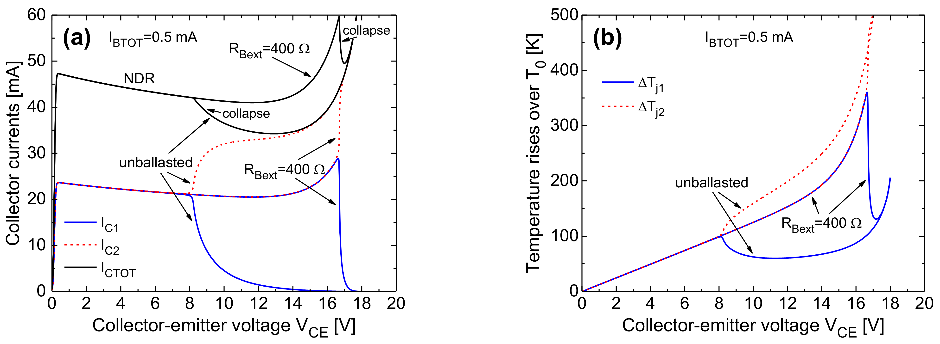
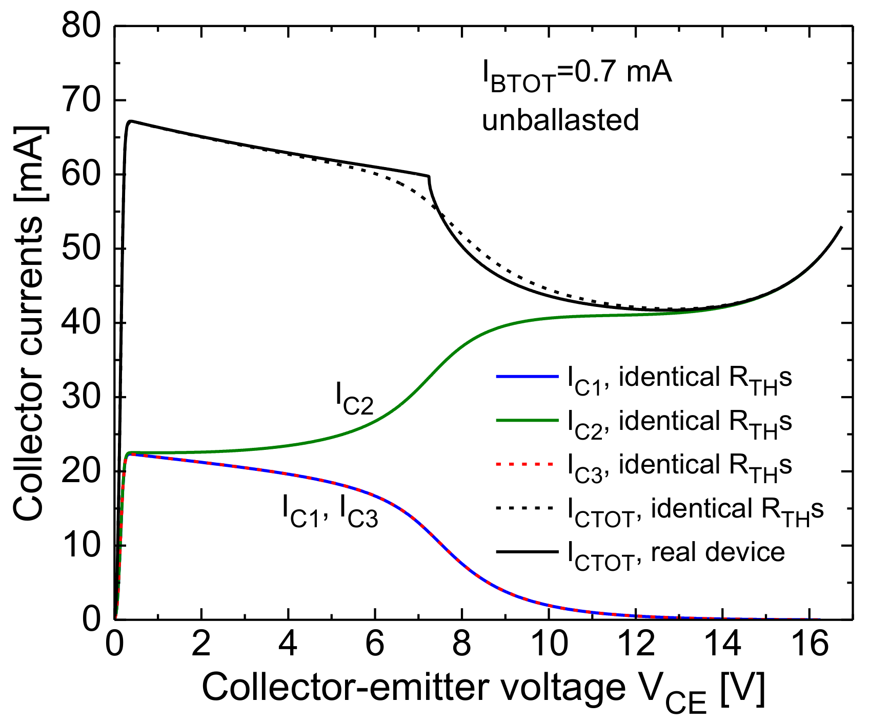
  • The collapse onset in an IBTOT-constant ICTOTVCE curve is associated to a uneven current/temperature distribution, wherein the right-column cells (in particular, the inner ones) bear almost all the current.
  • The steeper ICTOT drop in the collapse region is induced by a bifurcation mechanism involving the symmetric cells belonging to the right column. In the base-ballasted case (with RBext = 400 Ω) this leads to three adjacent cells conducting all the current (either the top or the bottom ones, depending on small technological/layout discrepancies); a further VCE increase makes the current flow in two cells, and eventually in only one cell (the outer one). In the unballasted and emitter-ballasted case (with REext = 4 Ω), for VCE slightly higher than that entailing the bifurcation, the current flows in only one of the inner cells (#9 or #10). This leads to a very sharp and linear temperature increment vs. VCE of this cell (plainly illustrated for cell #9 in Figure 23b).
  • Such a linear nature of the ΔTj9–VCE behavior can be straightforwardly explained as follows. Neglecting II effects, which is reasonable in both the unballasted and emitter-ballasted cases, ΔTj9 is approximately equal to RTH99(Tj9)·βF(Tj9IBTOT·VCE + 58 K (IB9IBTOT), where RTH99 is the SH thermal resistance of cell #9, and 58 K is the difference between TB and T0; as VCE increases, there is a compensation between the NTC of βF and the increase in RTH99 with temperature due to nonlinear thermal effects.
We shall now focus on half of the 28-cell array; all cells are base-ballasted with RBext = 400 Ω. Figure 24 depicts the PSPICE results obtained under CE conditions for IBTOT = 3.5 mA. It is found that beyond VCE = 8.5 V the current distribution becomes uneven, leading to the onset of collapse in the ICTOTVCE curve. The right-column cells (#8 to #14) carry all the current, while the left-column counterparts (#1 to #7) turn off. In particular, the current is mostly conducted by the inner cells: the highest by the innermost #11, a slightly lower one by each of the symmetric cells #10, #12, an even lower by #9, #13, and so on. At VCE = 10.8 V, a bifurcation occurs for these symmetric pairs, and #10, #9, and #8 prevail over #12, #13, and #14, so that only the top group composed by the adjacent #8 to #11 cells conducts. Further increasing VCE, the current would first focus over the 3-cell group #8 to #10, then over the pair #8, #9, and would eventually flow only in the outermost cell #8, which is affected by the highest RTH. On the other hand, the reduction in the number of conducting top cells is found to occur after the temperature rise of cells #11, #10, and #9 has well exceeded 600 K; consequently, in the practical case, the metallization and dielectrics over such cells are expected to lose their integrity when still the whole group #8 to #11 is conducting.
As mentioned in Section 3.5, unlike conventional ETNs, the one derived by FANTASTIC allows the reconstruction of the whole linear temperature rise field ΔTlin(x, y, z) = Tlin(x, y, z) − T0, which can be easily processed through the calibrated Kirchhoff’s transformation to get the nonlinear ΔT(x, y, z), for selected biasing conditions. Figure 25 shows the ΔT(x, y, z) map for half of the 28-cell array biased with IBTOT = 3.5 mA and VCE equal to 6 V (as representative of the uniform operating region), 10 V (collapse region: all the right-column cells are conducting), and 13.3 V (deep/marked collapse: after the bifurcation mechanism, the current flows only through the group #8 to #11).
Lastly, an interesting and fair comparison is performed between the halved portions of the base-ballasted 24- and 28-cell arrays by applying various IBTOT values ensuring the same total base current density JBTOT = IBTOT/AETOT in both cases. Results are reported in Figure 26; more specifically, Figure 26a shows the JCTOTVCE characteristic (JCTOT = ICTOT/AETOT), and Figure 26b depicts the junction temperature rise of cell #9 for the 24-cell array, and of cell #11 for the 28-cell one. The analysis demonstrates that the 28-cell array featuring an odd number of cells (seven) per column is less thermally robust than the 24-cell counterpart with an even number of cells (six) per column (the collapse locus is shifted leftward). This is attributed to the fact that the nonuniform current/temperature distribution triggering the collapse in the 28-cell structure implies that the innermost cell #11 takes more current than the others, while two cells (#9 and #10) concurrently bear this task in the 24-cell array. It is worth noting that, although this seems to be an expected results, there are still many designers using arrays with an odd number of cells per column.

5. Conclusions

In this paper, an efficient simulation approach has been used to analyze the dc electrothermal behavior of test devices and arrays for output stages of power amplifiers in InGaP/GaAs HBT technology. The approach relies on a full circuit representation of the structures under investigation (also referred to as macrocircuit), the solution of which can be evaluated by any circuit simulation software and requires tens of seconds at most, despite the complexity of the analysis. The macrocircuit is based on the thermal equivalent of the Ohm’s law, and includes subcircuits to describe the unit cells, as well as a thermal feedback block to account for the power-temperature feedback. The thermal feedback block is obtained by combining (i) a FEM thermal tool aided by an in-house routine to generate an exceptionally accurate 3-D geometry/mesh of the structure, (ii) the FANTASTIC code to automatically get an equivalent thermal network without the need of simulations or user’s experience, (iii) a preliminarily-calibrated Kirchhoff’s transformation to include nonlinear thermal effects. The test devices have been analyzed under all the bias conditions of interest. An overview has been given on the thermally- and avalanche-induced distortion in the I–V characteristics, the limits of the safe behavior have been identified, and the beneficial effect of base ballasting has been explored. As far as the HBT arrays are concerned, the approach better shows its potential, as the individual currents, temperatures, and key parameters of all unit cells can be monitored. Some of the most important findings are: the base ballasting has been found to be more effective than emitter ballasting, which is typically suggested for breakdown-limited bipolar transistors; the arrays are more thermally-robust if arranged in columns with an even number of unit cells, where two central cells concurrently bear the heat coming from the outer ones as a nonuniform operating condition occurs. The approach is well suited to support engineers and designers in making choices oriented to develop more thermally-rugged and reliable circuits through, e.g., layout and/or nonuniform ballasting optimization.

Author Contributions

Methodology, V.d.; Software, V.d., A.P.C., C.S. and L.C.; Investigation, V.d., P.J.Z.; Writing—Original Draft Preparation, V.d.; Writing—Review and Editing, V.d.; Supervision, V.d., and P.J.Z. All authors have read and agreed to the published version of the manuscript.

Funding

This research received no external funding.

Data Availability Statement

Not applicable.

Acknowledgments

The funding for the Ph.D. activity of Ciro Scognamillo was generously donated by the Rinaldi family in the memory of Niccolò Rinaldi, a bright Professor and Researcher of University of Naples Federico II, prematurely passed away in 2018.

Conflicts of Interest

The authors declare no conflict of interest.

Nomenclature

CBcommon base
CEcommon emitter
DCTMdynamic compact thermal model
DoFdegree of freedom
ETelectrothermal
ETNequivalent thermal network
FANTASTICFAst Novel Thermal Analysis Simulation Tool for Integrated Circuits
FEMfinite-element method
GaAsgallium arsenide
HBTheterojunction bipolar transistor
HIhigh injection
IIimpact ionization (avalanche)
MORmodel-order reduction
NDRnegative differential resistance
NTCnegative temperature coefficient
PApower amplifier
PTCpositive temperature coefficient
RTHthermal resistance [K/W]
SCRspace-charge region
SCTMstatic compact thermal model
SHself-heating
SOGsilicon-on-glass
TEOLthermal equivalent of the Ohm’s law
TFBthermal feedback block
T0reference temperature: 300 K
TBtemperature of the laminate bottom for the arrays: 358 K
Tjtemperature averaged over the base-emitter junction under nonlinear thermal conditions
Tjlintemperature averaged over the base-emitter junction under linear thermal conditions
ΔTjtemperature rise Tj-T0
ΔTjlintemperature rise Tjlin-T0
ΔTjBtemperature rise Tj-TB
ΔTjlinBtemperature rise Tjlin-TB

References

  1. Fresina, M. Trends in GaAs HBTs for wireless and RF. In Proceedings of the IEEE Bipolar/BiCMOS Circuits and Technology Meeting (BCTM), Atlanta, GA, USA, 9–11 October 2011; pp. 150–153. [Google Scholar]
  2. Zarębski, J.; Górecki, K. SPICE-aided modelling of dc characteristics of power bipolar transistors with self-heating taken into account. Int. J. Numer. Model. 2009, 22, 422–433. [Google Scholar] [CrossRef]
  3. Zarębski, J.; Górecki, K. The electrothermal large-signal model of power MOS transistors for SPICE. IEEE Trans. Power Electron. 2010, 25, 1265–1274. [Google Scholar] [CrossRef]
  4. Górecki, K.; Górecki, P. Modelling dynamic characteristics of the IGBT with thermal phenomena taken into account. Microelectron. Int. 2017, 34, 160–164. [Google Scholar] [CrossRef]
  5. Nenadović, N.; d’Alessandro, V.; La Spina, L.; Rinaldi, N.; Nanver, L.K. Restabilizing mechanisms after the onset of thermal instability in bipolar transistors. IEEE Trans. Electron Devices 2006, 53, 643–653. [Google Scholar] [CrossRef]
  6. La Spina, L.; d’Alessandro, V.; Russo, S.; Rinaldi, N.; Nanver, L.K. Influence of concurrent electrothermal and avalanche effects on the safe operating area of multifinger bipolar transistors. IEEE Trans. Electron Devices 2009, 56, 483–491. [Google Scholar] [CrossRef]
  7. La Spina, L.; d’Alessandro, V.; Russo, S.; Nanver, L.K. Thermal design of multifinger bipolar transistors. IEEE Trans. Electron Devices 2010, 57, 1789–1800. [Google Scholar] [CrossRef]
  8. Metzger, A.G.; d’Alessandro, V.; Rinaldi, N.; Zampardi, P.J. Evaluation of thermal balancing techniques in InGaP/GaAs HBT power arrays for wireless handset power amplifiers. Microelectron. Reliab. 2013, 53, 1471–1475. [Google Scholar] [CrossRef]
  9. Rinaldi, N.; d’Alessandro, V. Analysis of the bipolar current mirror including electrothermal and avalanche effects. IEEE Trans. Electron Devices 2009, 56, 1309–1321. [Google Scholar] [CrossRef]
  10. D’Alessandro, V.; de Magistris, M.; Magnani, A.; Rinaldi, N.; Grivet-Talocia, S.; Russo, S. Time domain dynamic electrothermal macromodeling for thermally aware integrated system design. In Proceedings of the IEEE workshop on Signal and Power Integrity (SPI), Paris, France, 12–15 May 2013. [Google Scholar]
  11. D’Alessandro, V.; La Spina, L.; Nanver, L.K.; Rinaldi, N. Analysis of electrothermal effects in bipolar differential pairs. IEEE Trans. Electron Dev. 2011, 58, 966–978. [Google Scholar] [CrossRef]
  12. D’Alessandro, V.; de Magistris, M.; Magnani, A.; Rinaldi, N.; Russo, S. Dynamic electrothermal analysis of bipolar devices and circuits relying on multi-port positive Foster representation. In Proceedings of the IEEE Bipolar/BiCMOS Circuits and Technology Meeting (BCTM), Portland, OR, USA, 30 September–3 October 2012. [Google Scholar]
  13. D’Alessandro, V.; D’Esposito, R.; Metzger, A.G.; Kwok, K.H.; Aufinger, K.; Zimmer, T.; Rinaldi, N. Analysis of electrothermal and impact-ionization effects in bipolar cascode amplifiers. IEEE Trans. Electron Devices 2018, 65, 431–439. [Google Scholar] [CrossRef]
  14. D’Alessandro, V.; Magnani, A.; Riccio, M.; Breglio, G.; Irace, A.; Rinaldi, N.; Castellazzi, A. SPICE modeling and dynamic electrothermal simulation of SiC power MOSFETs. In Proceedings of the IEEE International Symposium on Power Semiconductor Devices and ICs (ISPSD), Waikoloa, HI, USA, 15–19 June 2014; pp. 285–288. [Google Scholar]
  15. D’Alessandro, V.; Catalano, A.P.; Codecasa, L.; Moser, B.; Zampardi, P.J. Combined SPICE-FEM analysis of electrothermal effects in InGaP/GaAs HBT devices and arrays for handset applications. In Proceedings of the IEEE International Conference on Thermal, Mechanical and Multi-Physics Simulation and Experiments in Microelectronics and Microsystems (EuroSimE), Toulouse, France, 15–18 April 2018. [Google Scholar]
  16. COMSOL Multiphysics User’s Guide, Release 5.2A. 2016. Available online: https://www.comsol.it/ (accessed on 1 October 2020).
  17. D’Alessandro, V.; Catalano, A.P.; Codecasa, L.; Zampardi, P.J.; Moser, B. Accurate and efficient analysis of the upward heat flow in InGaP/GaAs HBTs through an automated FEM-based tool and Design of Experiments. Int. J. Numer. Model. Electron. Netw. Devices Fields 2019, 32, e2530. [Google Scholar] [CrossRef]
  18. Carlslaw, H.S.; Jaeger, J.C. Conduction of Heat in Solids, 2nd ed.; Oxford University Press: London, UK, 1959. [Google Scholar]
  19. Joyce, W.B. Thermal resistance of heat sinks with temperature-dependent conductivity. Solid State Electron. 1975, 18, 321–322. [Google Scholar] [CrossRef]
  20. PSPICE User’s Manual, Cadence OrCAD 16.5. 2011. Available online: https://www.orcad.com/ (accessed on 1 October 2020).
  21. D’Alessandro, V.; Codecasa, L.; Catalano, A.P.; Scognamillo, C. Circuit-based electrothermal simulation of multicellular SiC power MOSFETs using FANTASTIC. Energies 2020, 13, 4563. [Google Scholar] [CrossRef]
  22. Codecasa, L.; d’Alessandro, V.; Magnani, A.; Rinaldi, N.; Zampardi, P.J. FAst novel thermal analysis simulation tool for integrated circuits (FANTASTIC). In Proceedings of the International workshop on THERMal INvestigations of ICs and systems (THERMINIC), London, UK, 24–26 September 2014. [Google Scholar]
  23. Magnani, A.; d’Alessandro, V.; Codecasa, L.; Zampardi, P.J.; Moser, B.; Rinaldi, N. Analysis of the influence of layout and technology parameters on the thermal impedance of GaAs HBT/BiFET using a highly-efficient tool. In Proceedings of the IEEE Compound Semiconductor Integrated Circuit Symposium (CSICS), La Jolla, CA, USA, 19–22 October 2014. [Google Scholar]
  24. D’Alessandro, V.; Catalano, A.P.; Magnani, A.; Codecasa, L.; Rinaldi, N.; Moser, B.; Zampardi, P.J. Simulation comparison of InGaP/GaAs HBT thermal performance in wire-bonding and flip-chip technologies. Microelectron. Reliab. 2017, 78, 233–242. [Google Scholar] [CrossRef]
  25. Zhang, Q.M.; Hu, H.; Sitch, J.; Surridge, R.K.; Xu, J.M. A new large signal HBT model. IEEE Trans. Microw. Theory Tech. 1996, 44, 2001–2009. [Google Scholar] [CrossRef]
  26. Liu, W.; Khatibzadeh, A. The collapse of current gain in multi-finger heterojunction bipolar transistors: Its substrate temperature dependence, instability criteria, and modeling. IEEE Trans. Electron. Devices 1994, 41, 1698–1707. [Google Scholar] [CrossRef]
  27. Nenadović, N.; d’Alessandro, V.; Nanver, L.K.; Tamigi, F.; Rinaldi, N.; Slotboom, J.W. A back-wafer contacted silicon-on-glass integrated bipolar process–Part II: A novel analysis of thermal breakdown. IEEE Trans. Electron. Devices 2004, 51, 51–62. [Google Scholar] [CrossRef]
  28. D’Alessandro, V.; Marano, I.; Russo, S.; Céli, D.; Chantre, A.; Chevalier, P.; Pourchon, F.; Rinaldi, N. Impact of layout and technology parameters on the thermal resistance of SiGe:C HBTs. In Proceedings of the IEEE Bipolar/BiCMOS Circuits and Technology Meeting (BCTM), Austin, TX, USA, 4–6 October 2010; pp. 137–140. [Google Scholar]
  29. D’Alessandro, V.; Sasso, G.; Rinaldi, N.; Aufinger, K. Influence of scaling and emitter layout on the thermal behavior of toward-THz SiGe:C HBTs. IEEE Trans. Electron. Devices 2014, 61, 3386–3394. [Google Scholar] [CrossRef] [Green Version]
  30. Miller, S.L. Ionization rates for holes and electrons in silicon. Phys. Rev. 1957, 105, 1246–1249. [Google Scholar] [CrossRef]
  31. Rinaldi, N.; d’Alessandro, V. Theory of electrothermal behavior of bipolar transistors: Part III–Impact ionization. IEEE Trans. Electron Devices 2006, 53, 1683–1697. [Google Scholar] [CrossRef]
  32. Zampardi, P.J.; Yang, Y.; Hu, J.; Li, B.; Fredriksson, M.; Kwok, K.H.; Shao, H. Practical statistical simulation for efficient circuit design. In Nonlinear Transistor Model Parameter Extraction Techniques; Chapter 9; Rudolph, M., Fager, C., Root, D.E., Eds.; Cambridge University Press: Cambridge, UK, 2011; pp. 287–317. [Google Scholar]
  33. Palankovski, V.; Quay, R. Analysis and Simulation of Heterostructure Devices; Springer: New York, NY, USA, 2004. [Google Scholar]
  34. Anholt, R. HBT thermal element design using an electro/thermal simulator. Solid State Electron. 1998, 42, 857–864. [Google Scholar] [CrossRef]
  35. Lienhard, J.H., IV; Lienhard, J.H., V. A Heat Transfer Textbook; Phlogiston Press: Cambridge, MA, USA, 2008. [Google Scholar]
  36. Poulton, K.; Knudsen, K.L.; Corcoran, J.J.; Wang, K.-C.; Pierson, R.L.; Nubling, R.B.; Chang, M.-C.F. Thermal design and simulation of bipolar integrated circuits. IEEE J. Solid State Circuits 1992, 27, 1379–1387. [Google Scholar] [CrossRef]
  37. Codecasa, L.; D’Amore, D.; Maffezzoni, P. Compact modeling of electrical devices for electrothermal analysis. IEEE Trans. Circuits Syst. I 2003, 50, 465–476. [Google Scholar] [CrossRef]
  38. Codecasa, L.; Catalano, A.P.; d’Alessandro, V. A priori error bound for moment matching approximants of thermal models. IEEE Trans. Comp. Packag. Manufact. Technol. 2019, 9, 2383–2392. [Google Scholar] [CrossRef]
  39. Keysight Advanced Design System (ADS). 2019. Available online: https://edadocs.software.keysight.com/ads2019 (accessed on 25 January 2021).
  40. Schröter, M.; Chakravorty, A. Compact Hierarchical Bipolar Transistor Modeling with HICUM; World Scientific Publishing: Singapore, 2010. [Google Scholar]
  41. Keysight ADS Electro-Thermal Simulator (Agilent EEsof EDA). Available online: https://www.keysight.com/upload/cmc_upload/All/ADSElectrothermal.pdf (accessed on 25 January 2021).
  42. Dawson, D.E.; Gupta, A.K.; Salib, M.L. CW measurements of HBT thermal resistance. IEEE Trans. Electron Devices 1992, 39, 2235–2239. [Google Scholar] [CrossRef]
  43. Popescu, C. Selfheating and thermal runaway phenomena in semiconductor devices. Solid State Electron. 1970, 13, 441–450. [Google Scholar] [CrossRef]
  44. Latif, M.; Bryant, P.R. Multiple equilibrium points and their significance in the second breakdown of bipolar transistors. IEEE J. Solid State Circuits 1981, 16, 8–15. [Google Scholar] [CrossRef]
  45. Rinaldi, N.; d’Alessandro, V. Theory of electrothermal behavior of bipolar transistors: Part I–Single-finger devices. IEEE Trans. Electron Devices 2005, 52, 2009–2021. [Google Scholar] [CrossRef]
  46. Jaoul, M.; Céli, D.; Maneux, C.; Zimmer, T. Measurement based accurate definition of the SOA edges for SiGe HBTs. In Proceedings of the IEEE BiCMOS and Compound semiconductor Integrated Circuits and Technology Symposium (BCICTS), Nashville, TN, USA, 3–6 November 2019. [Google Scholar]
  47. Liu, W.; Khatibzadeh, A.; Sweder, J.; Chau, H.-F. The use of base ballasting to prevent the collapse of current gain in AlGaAs/GaAs heterojunction bipolar transistors. IEEE Trans. Electron Devices 1996, 43, 245–251. [Google Scholar] [CrossRef]
  48. Vanhoucke, T.; Hurkx, G.A.M. Unified electro-thermal stability criterion for bipolar transistors. In Proceedings of the IEEE Bipolar/BiCMOS Circuits and Technology Meeting (BCTM), Santa Barbara, CA, USA, 9–11 October 2005; pp. 37–40. [Google Scholar]
  49. Seiler, U.; Koenig, E.; Narozny, P.; Dämbkes, H. Thermally triggered collapse of collector current in power heterojunction bipolar transistors. In Proceedings of the IEEE Bipolar/BiCMOS Circuits and Technology Meeting (BCTM), Minneapolis, MN, USA, 4–5 October 1993; pp. 257–260. [Google Scholar]
  50. Liu, W.; Nelson, S.; Hill, D.G.; Khatibzadeh, A. Current gain collapse in microwave multifinger heterojunction bipolar transistors operated at very high power densities. IEEE Trans. Electron Devices 1993, 40, 1917–1927. [Google Scholar] [CrossRef]
  51. Liu, W. Thermal coupling in 2-finger heterojunction bipolar transistors. IEEE Trans. Electron Devices 1995, 42, 1033–1038. [Google Scholar] [CrossRef]
  52. Wang, K.-C.; Asbeck, P.M.; Chang, M.-C.F.; Miller, D.L.; Sullivan, G.J.; Corcoran, J.J.; Hornak, T. Heating effects on the accuracy of HBT voltage comparators. IEEE Trans. Electron Devices 1987, 34, 1729–1735. [Google Scholar] [CrossRef]
  53. Järvinen, E.; Kalajo, S.; Matilainen, M. Bias circuits for GaAs HBT power amplifiers. In Proceedings of the IEEE MTT-S International Microwave Symposium Digest, Phoenix, AZ, USA, 20–24 May 2001; pp. 507–510. [Google Scholar]
  54. Zampardi, P.J. Silicon modelers are from Mars, GaAs modelers are from Venus. In Proceedings of the IEEE Bipolar/BiCMOS Circuits and Technology Meeting (BCTM), Miami, FL, USA, 19–21 October 2017; pp. 257–260. [Google Scholar]
Figure 1. Schematic cross-section of the HBT unit cell highlighting the materials, the base-emitter junction, and the base-collector space-charge region (SCR).
Electronics 10 00757 g001
Figure 2. Schematic layouts of all the structures analyzed in this work: (top) 1-, 2-, 3-cell test devices; (bottom) 24- and 28-cell arrays. As clarified in Section 3.4, only half of the arrays (comprising 12 and 14 unit cells, respectively) was thermally and electrothermally simulated.
Electronics 10 00757 g002
Figure 3. Simplified representation of the SPICE-compatible unit-cell subcircuit implementing the analytical model described in Section 3.2.
Electronics 10 00757 g003
Figure 4. (Left) Single-cell test device built in the COMSOL environment (draw mode); as can be seen, the pads are arranged in a ground-signal-ground configuration to allow for RF experimental characterization. (Right) Magnification of the unit cell.
Electronics 10 00757 g004
Figure 5. (Left) Two-cell test device built in the COMSOL environment (mesh mode). The numbers of elements (tetrahedra) and degrees of freedom (DoFs) are 2.4 × 10⁶ and 3.3 × 10⁶, respectively. (Right) Magnification of the two unit cells. A horizontally-large substrate (not fully represented in the figure) was considered to safely neglect the effect of the lateral adiabatic sides on the temperature field over the base-emitter junction.
Electronics 10 00757 g005
Figure 6. (Left) Half of the 24-cell array (with six cells per column) constructed in the COMSOL environment (draw mode). (Right) Magnification of the die; evidenced is the single unit cell.
Electronics 10 00757 g006
Figure 7. (Left) Half of the 28-cell array (with seven cells per column) built in the COMSOL environment (mesh mode). The numbers of tetrahedra and DoFs are 3.7 × 10⁶ and 4.9 × 10⁶, respectively. (Right) Magnification of some unit cells.
Electronics 10 00757 g007
Figure 8. Test device with single unit cell: junction temperature rise over T0 vs. dissipated power PD, as evaluated by COMSOL under linear (solid blue line) and nonlinear (red symbols) conditions, along with that computed by applying the Kirchhoff’s transformation (10) with calibrated mk = 0.8333 (solid green line) to the linear COMSOL temperature rise.
Electronics 10 00757 g008
Figure 9. Equivalent thermal network (ETN) determined by FANTASTIC under linear thermal conditions.
Electronics 10 00757 g009
Figure 10. Sketch of the merely-electrical macrocircuit including ET effects through the TEOL. The paralleled (sharing the same base, emitter, collector contacts) subcircuits describing the unit cells are connected to the TFB containing: the ETN preliminarily evaluated by FANTASTIC, the calibrated Kirchhoff’s transformation, and a block adding 58 K (for the arrays only).
Electronics 10 00757 g010
Figure 11. Test device with single unit cell: simulated (a) collector current IC and (b) corresponding temperature rise ΔTj above T0 against collector-emitter voltage VCE for VBE = 1.25, 1.3, 1.35, 1.4, 1.45 V. The unballasted case (red lines) is compared to the one with RBext = 400 Ω connected to the base (black).
Electronics 10 00757 g011
Figure 12. Test device with two unit cells: simulated (a) collector currents and (b) temperature rises over T0 vs. collector-emitter voltage VCE for IBTOT = 0.5 mA. Both the unballasted case and that ballasted with RBext = 400 Ω per cell are reported.
Electronics 10 00757 g012
Figure 13. Unballasted test device with two unit cells: simulated (a) collector currents and (b) temperature rises over T0 vs. collector-emitter voltage VCE for VBE = 1.2, 1.25, 1.3 V.
Electronics 10 00757 g013
Figure 14. Ballasted (with RBext = 400 Ω) test device with two unit cells: simulated (a) collector currents and (b) junction temperature rises over T0 vs. collector-emitter voltage VCE for VBE = 1.2, 1.25, 1.3 V.
Electronics 10 00757 g014
Figure 15. Test device with two unit cells: simulated (a) collector currents and (b) junction temperature rises over T0 vs. total collector current IETOT for VCB = 8 V. Both the unballasted and ballasted (with RBext = 400 Ω per each unit cell) devices are considered. In (b), ΔTj1 increases beyond IETOT = 43 mA due to the thermal coupling with cell #2.
Electronics 10 00757 g015
Figure 16. Test device with three unit cells, either unballasted or ballasted with RBext = 400 Ω per cell: simulated (a) collector currents and (b) junction temperature rises over T0 vs. collector-emitter voltage VCE.
Electronics 10 00757 g016
Figure 17. Simulated ICTOTVCE characteristics for the unballasted (red) and ballasted (black) 3-cell test device for IBTOT = 0.7, 1.2, 1.7, 2.2, 2.7 mA.
Electronics 10 00757 g017
Figure 18. Unballasted 3-cell test device with unit cells sharing ideally identical SH RTHs: simulated collector currents against collector-emitter voltage VCE. Also shown is the ICTOTVCE characteristic corresponding to the real structure (solid black line).
Electronics 10 00757 g018
Figure 19. Simulated (a) collector currents and (b) junction temperature rises above T0 for the 12 cells of half of the 24-cell array ballasted with RBext = 400 Ω per cell, and biased with IBTOT = 2 mA.
Electronics 10 00757 g019
Figure 20. Simulated (a) collector currents and (b) junction temperature rises above T0 for the 12 cells of the halved 24-cell array ballasted with RBext = 400 Ω per cell, with IBTOT = 3 mA applied.
Electronics 10 00757 g020
Figure 21. Simulated (a) collector currents and (b) junction temperature rises over T0 vs. collector-emitter voltage VCE for half of the unballasted 24-cell array biased with IBTOT = 3 mA.
Electronics 10 00757 g021
Figure 22. Simulated (a) collector currents and (b) junction temperature rises above T0 for the 12 cells of the halved 24-cell array ballasted with REext = 4 Ω per cell, and biased with IBTOT = 3 mA.
Electronics 10 00757 g022
Figure 23. Simulated (a) total collector currents and (b) junction temperature rises above T0 of cell #9 against collector-emitter voltage VCE for half of the 24-cell array biased with IBTOT = 1, 1.5, 2, 2.5, 3, 3.5, 4, 4.5, 5 mA. Comparison between the case with no ballasting (red lines), and those benefiting from RBext = 400 Ω (black) and REext = 4 Ω (blue) per cell.
Electronics 10 00757 g023
Figure 24. Simulated (a) collector currents and (b) junction temperature rises above T0 for half of the ballasted 28-cell array biased with IBTOT = 3.5 mA.
Electronics 10 00757 g024
Figure 25. Spatial temperature rise map ΔT(x, y, z) over half of the 28-cell array, as reconstructed by FANTASTIC equipped with the Kirchhoff’s transformation for IBTOT = 3.5 mA and VCE equal to (a) 6, (b) 10, and (c) 13.3 V.
Electronics 10 00757 g025
Figure 26. Simulated (a) total collector current densities JCTOT and (b) junction temperature rises above T0 of cell #9 (black lines) and #11 (red lines) for the 24- and 28-cell arrays, respectively, vs. collector-emitter voltage VCE. The halved 24-cell array was biased with IBTOT = 1, 1.5, 2, 2.5, 3, 3.5, 4, 4.5, 5 mA, while the halved 28-cell one with IBTOT = 1.17, 1.75, 2.33, 2.91, 3.5, 4.08, 4.67, 5.25, 5.83 mA.
Electronics 10 00757 g026
Table 1. Key features of the investigated HBT technology.
ParameterValue
Common-emitter current gain at 300 K and medium current levels βF0135
Open-emitter breakdown voltage BVCBO27 V
Open-base breakdown voltage BVCEO17 V
Peak cut-off frequency fT for VCE = 3 V40 GHz
Collector current density JC at peak fT for VCE = 3 V0.2 mA/µm2
Maximum oscillation frequency fMAX82 GHz
Table 2. Model parameter values.
ParameterValue
AE164 µm2
JS03.5 × 10−26 A/µm2
η1.01
VAF1000 V
βF0135
ϕ05.4 mV/K
ΔEG/k200 K−1
JHI0.35 mA/µm2
nHI1
BVCBO27 V
nAV9 [32]
RE1 Ω
RB3.5 Ω
Table 3. Thermal conductivities of the materials composing the devices and arrays.
Materialk(T0)
(W/µmK)
k(TB)
(W/µmK)
Temperature Dependence
Si3N418.5 × 10−6 [33]19.6 × 10⁻⁶(8), α = −0.33 [33]
In0.5Ga0.5As0.048 × 10−4 [33]3.9 × 10⁻⁶(8), α = 1.175 [33]
InxGa1-xAs
(0 < x< 0.5)
0.092 × 10⁻⁴ [33]
average in the layer
7.4 × 10⁻⁶(8), α = 1.212 [33]
GaAs4.6 × 10−5 [33]3.69 × 10⁻⁵(8), α = 1.25 [33]
ion-implanted GaAs0.046 × 10−5 [33]0.0369 × 10⁻⁵(8), α = 1.25 [33]
In0.49Ga0.51P0.052 × 10−4 [33]0.041 × 10⁻⁴(8), α = 1.4 [33]
Au3.18 × 10−4 [34,35]3.14 × 10⁻⁴(9), β = 6.98 × 10⁻⁸ W/μmK2
[34,35]
Pt0.71 × 10−4 [34,35]0.71 × 10⁻⁴independent
Ti0.22 × 10−4 [34,35]0.22 × 10⁻⁴independent
Ni0.91 × 10−4 [35]0.863 × 10⁻⁴(9), β = 8.1 × 10⁻⁸ W/μmK2 [35]
Ge0.6 × 10−4 [33]0.48 × 10⁻⁴(8), α = 1.25 [33]
Cu3.98 × 10−4 [35]3.95 × 10⁻⁴(9), β = 5.83 × 10⁻⁸ W/μmK2 [35]
Glue1 × 10−41 × 10−4independent
Polybenzoxazole (PBO)0.0014 × 10−40.0014 × 10−4independent
laminate dielectric0.0065 × 10−40.0065 × 10⁻⁴independent
Publisher’s Note: MDPI stays neutral with regard to jurisdictional claims in published maps and institutional affiliations.

