Article

Discrete Time Domain Modeling and Control of a Grid-Connected Four-Wire Split-Link Converter

by
Jeroen D. M. De Kooning
1,2,*,
Dimitar Bozalakov
1,3 and
Lieven Vandevelde
1,3
1
Department of Electromechanical, Systems and Metal Engineering, Ghent University, Tech Lane Ghent Science Park—Campus A, Technologiepark Zwijnaarde 131, 9052 Ghent, Belgium
2
FlandersMake@UGent—Corelab EEDT-MP, Flanders Make, 9052 Ghent, Belgium
3
FlandersMake@UGent—Corelab EEDT-DC, Flanders Make, 9052 Ghent, Belgium
*
Author to whom correspondence should be addressed.
Electronics 2021, 10(4), 506; https://doi.org/10.3390/electronics10040506
Submission received: 26 December 2020 / Revised: 16 February 2021 / Accepted: 18 February 2021 / Published: 21 February 2021

Abstract

:
Distributed generation (DG) allows the production of renewable energy where it is consumed, avoiding transport losses. It is envisioned that future DG units will become more intelligent, not just injecting power into the grid but also actively improving the power quality by means of active power filtering techniques. In this manner, voltage and current harmonics, voltage unbalance or over-voltages can be mitigated. To achieve such a smart DG unit, an appropriate multi-functional converter topology is required, with full control over the currents exchanged with the grid, including the neutral-wire current. For this purpose, this article studies the three-phase four-wire split-link converter. A known problem of the split-link converter is voltage unbalance of the bus capacitors. This mid-point can be balanced either by injecting additional zero-sequence currents into the grid, which return through the neutral wire, or by injecting a compensating current into the mid-point with an additional half-bridge chopper. For both methods, this article presents a discrete time domain model to allow controller design and implementation in digital control. Both techniques are validated and compared by means of simulation results and experiments on a test setup.

1. Introduction

Global renewable energy capacity reached 2533 GW in 2019, consisting of 1308 GW hydropower, 622 GW wind and 585 GW solar [1], the remainder being marine, bio and waste energy sources. Most hydropower sources are large installations with a high rated power, e.g., the Three Gorges Dam station reaches a total of 22.5 GW. Wind turbines are becoming larger as well, recently breaching the 10 MW barrier with the Vestas V164 and the Siemens Gamesa 10.0–193 DD. In contrast, solar power installations are usually a more distributed form of renewable energy production, as they are ideally suited for roof installation. Hence, no particular land area or geographical conditions are required. Also, PV installations are modular, i.e., the number of panels can be selected to achieve the desired energy yield or power rating. For these reasons, photovoltaic (PV) installations are a popular investment for households and small and medium enterprises. Photovoltaic installations are the most popular form of distributed generation (DG), although micro combined heat and power (CHP) units, small wind turbines and waste-to-energy systems are suited as DG sources as well.
Distributed generation allows the production of renewable energy where it is consumed, avoiding transport losses in the transmission and distribution grids. When combined with a battery storage system, consumers can become more independent of the distribution grid. Also, demand side management services can be offered for peak shaving, reducing strong power fluctuations and peak loads. It is envisioned that future DG units will become more intelligent. These smart DG units will not just inject power into the grid as is common practice today, but can also actively improve the power quality [2] or act as a distributed power quality sensor, gathering data for the distribution system operator (DSO) [3]. Their distributed nature and widespread in the distribution system makes DG units ideal devices for local power quality improvement and an important asset in future smart grids or microgrids. Moreover, as power quality issues such as voltage unbalance or over-voltage can be mitigated, more renewable sources can be integrated in the distribution system [4].
To achieve a smart DG unit capable of actively improving the power quality of the grid, it must be equipped with an active power filtering (APF) functionality. Several APF techniques use the neutral-wire current to compensate for voltage unbalance, over-voltage or harmonics, e.g., the harmonic current compensation technique [5], the damping-based droop control technique [6] or resistive harmonic voltage filtering [7]. To deploy these active power filtering techniques in three-phase DG units, the use of a four-wire converter is essential. Hence, an appropriate multi-functional converter topology is required to achieve a smart DG unit. Ideally, this topology has full control over the currents exchanged with the grid, including the neutral-wire current. Many converter topologies can be employed for this purpose, i.e., the four-leg converter or the split-link converter, with or without active balancing circuits [8,9].
Figure 1 shows the four-leg (top) and split-link (bottom) converter topologies. Both topologies contain six IGBT or MOSFET switches, denoted S 1 till S 6 , to form a three-phase inverter. A three-phase low-pass filter is used to attenuate high-frequency switching ripples. This filter consists of the three inductor coils L f and the capacitors C f , where the subscript f stands for ’filter’. A four-leg converter has two additional switches to form a fourth leg, connected to the grid’s neutral via an additional inductor. The split-link converter is an alternative four-wire topology, where the dc bus capacitor is split to form a mid-point where the neutral wire is connected directly.
Although the four-leg topology offers a better dc bus voltage use [10] compared to the split-link converter, the control of the four-leg converter is complex, since the control of the three phases cannot be decoupled from the control of the fourth leg [11,12]. Also, EMC problems have been reported with the four-leg topology due to parasitic capacitances [10]. For the above reasons, the split-link converter is deemed to be a more suitable topology for smart DG units, as it has a simpler topology and control [13,14]. The challenge is to keep the dc bus voltage equally shared between both capacitors, i.e., to balance this mid-point. This balancing can be achieved by means of an additional control loop based on the injection of zero-sequence currents [15,16], or by means of an additional active balancing circuit [10,17]. Both techniques have their advantages and drawbacks regarding ease of implementation, circuit complexity, control dynamics and mid-point balancing effectiveness. This article presents a discrete time domain model using the Z transformation for both mid-point balancing techniques to allow implementation in digital control. Both techniques are validated and compared, both in simulation and on an experimental setup.

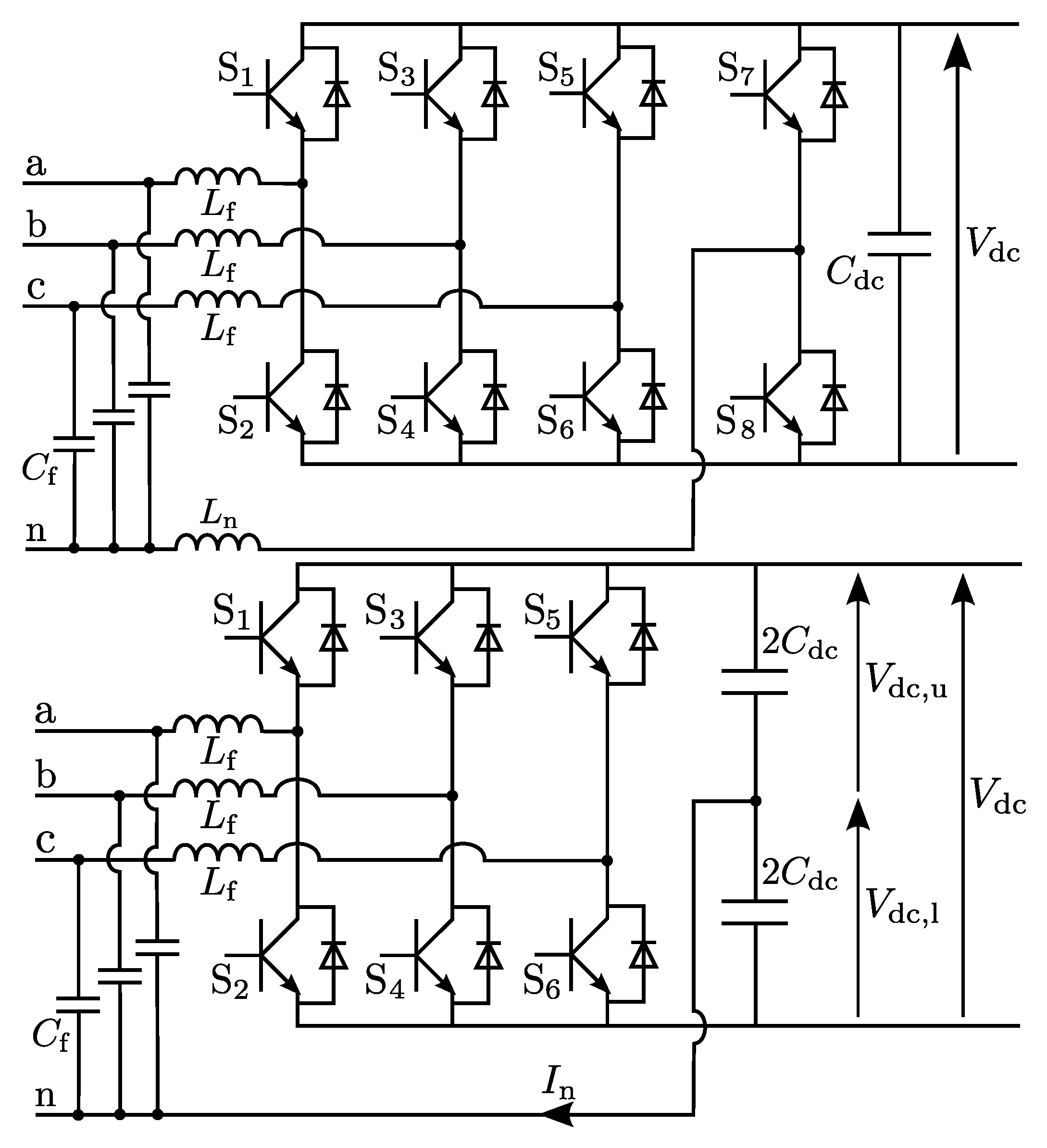
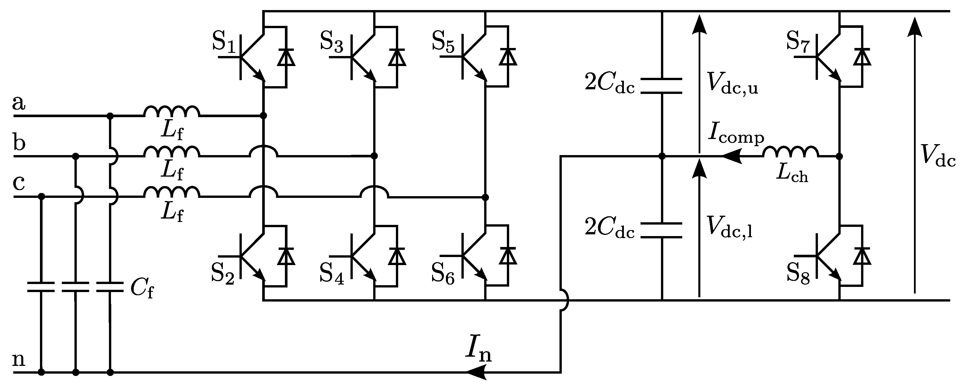
2. Split-Link Converter Topology and Control

This section discusses the problem of mid-point balancing in split-link converters. An overview of possible causes of mid-point unbalance is given, as well as an overview of the possible solutions.

2.1. Problem Statement

The dc link of the split-link converter, as shown in Figure 1, consists of two capacitors 2 C dc connected in series, resulting in a total bus capacitance of C dc . The mid-point feeds the neutral wire of the grid with a current I n . Ideally, the total dc bus voltage V dc is equally shared between both capacitors, i.e., the upper capacitor voltage V dc , u should equal V dc , l . However, there are a few possible reasons while the voltages deviate from this equal balance in practice [15,17]:
  • Unequal leakage currents of the capacitors
  • Unequal capacitor values
  • Unequal time delays during switching
  • Asymmetrical charging during transients
  • Current measurement errors
These issues can be solved by careful component selection or by using bleeder resistors, which are placed in parallel with the bus capacitors and help to retain an equal voltage. However, they consume active power and only compensate slow deviations due to their large time constant. The above reasons are minor causes of mid-point voltage unbalance, and usually result in a small deviation. In contrast, neutral-wire currents I n have a large impact on the mid-point voltage, and are thus the major cause of voltage unbalance [17]. The relation between the neutral-wire current I n and the voltage V dc , l on the lower capacitor can be expressed as follows:
V dc , l = 1 4 C dc I n ( t ) d t = 1 4 C dc s I n ( s )
where s is the Laplace operator. An ac component in I n results in an ac oscillation of the mid-point voltage, which does not disturb the proper functioning of the converter as long as it is limited. The capacitor value C dc should be chosen large enough to confine this ac component in V dc , l . In contrast, a dc component in I n has a considerable impact. Even a small dc current can cause a fast increase and severe dc error in V dc , l . This results in an inevitable failure of the converter. For instance, a dc current of 50 mA with a total bus capacitor of 1 mF creates a voltage deviation of −12.5 V/s. A dc current of 50 mA in the neutral wire is realistic, and can, e.g., be caused by offset errors in the current measurement, as will be shown further in this article.

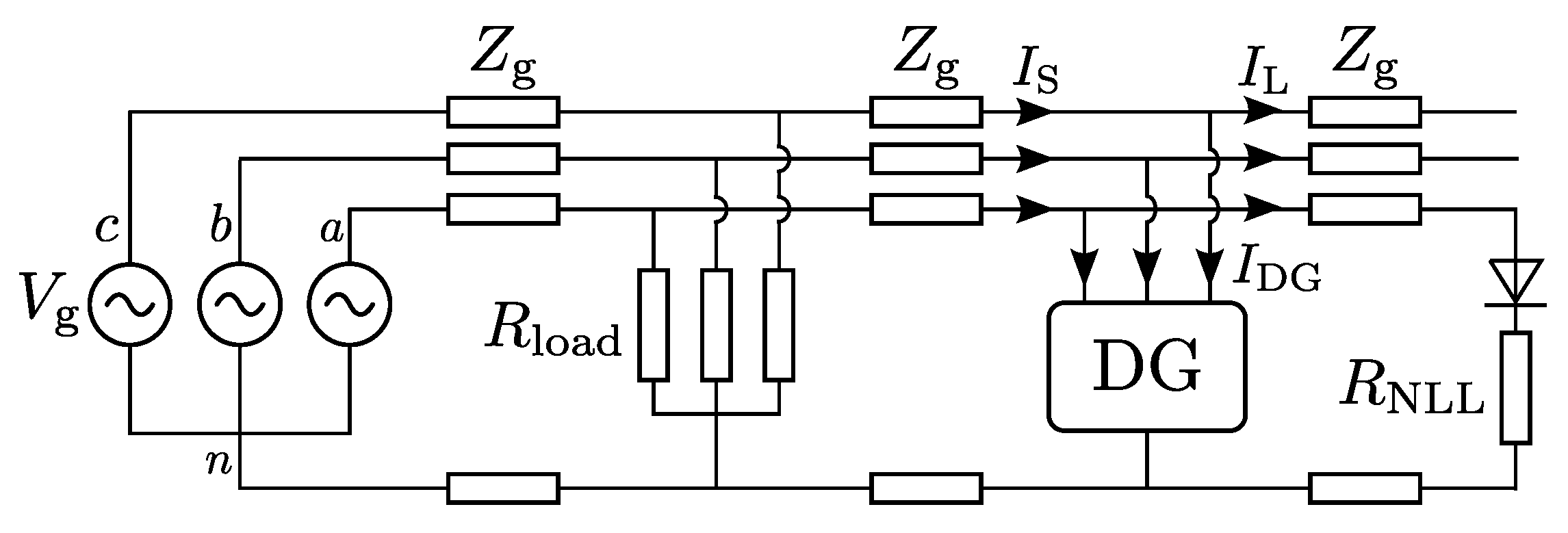
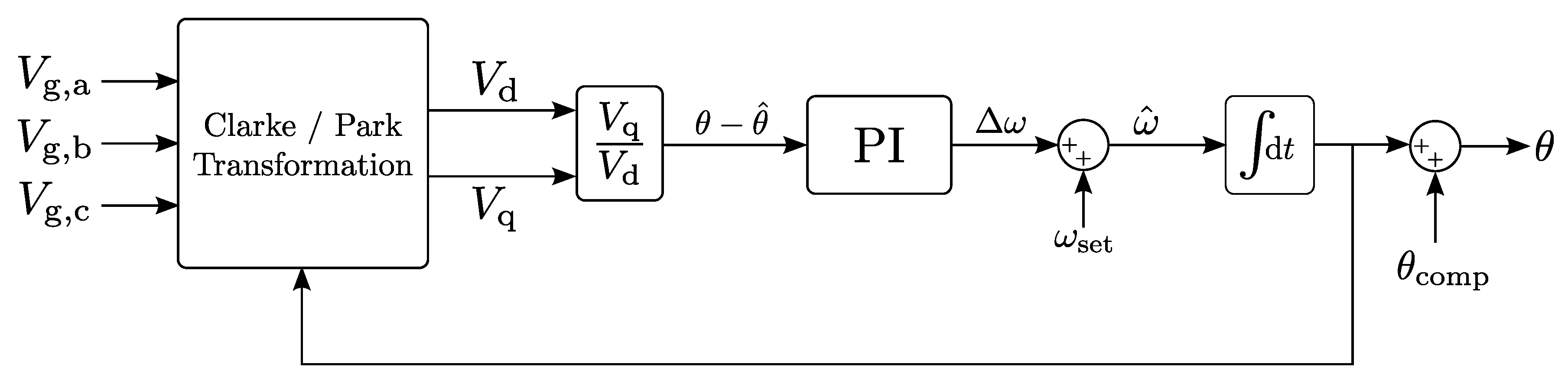
2.2. Origin of Neutral-Wire Currents

The origin and purpose of the neutral-wire current I n needs further explanation. For this, a simulation of a DG unit connected to a distribution grid will be performed using Matlab/Simulink. All electrical components of both the distribution grid and the power electronic converter are simulated by the Piecewise Linear Electrical Circuit Simulator (PLECS) power electronic toolbox for Simulink. Figure 2 shows the simulated distribution feeder. The voltage sources V g on the left produce an ideal set of three-phase symmetrical and sinusoidal voltages with a phase value of 230 V. The feeder contains a three-phase resistive load R load of 53 Ω. A DG unit is connected to the feeder, equipped with a four-wire split-link converter. Table 1 shows the parameters of the split-link converter used in the simulations. The renewable energy source is modeled as a dc current source I dc feeding the dc link of the converter with a current of 6 A. At the end of the feeder, a single-phase non-linear load (NLL) is connected. The non-linear load consists of a diode in series with a resistance R NLL of 50 Ω, forming a half-wave rectifier, which can be found in some consumer devices (e.g., hair dryers, two-level light dimmers and motor applications). This serves as an example of a non-linear load that results in dc currents in the grid. The resistance R NLL represents the heating resistance in a hair dryer or the light bulb in a light dimmer circuit. Also, cycloconverters and photovoltaic inverters can cause dc currents in the grid, especially if they are transformerless [18,19]. Between the devices on the feeder, the grid impedances of the phase and neutral wires are modeled according to 30 m of distribution cable of the BAXB type with an R / X value of 5.37. Table 2 shows the BAXB cable parameters used in the simulations. The feeder currents before the DG unit are labeled I S , the currents of the DG unit itself I DG and the feeder currents after the DG unit I L .
Figure 3 shows the control scheme of the split-link converter used for this simulation. Here, all quantities are in the time domain, i.e., they are not phasor representations. Time-domain variables in absolute quantities are written by using large letters, where variables in relative quantities are written by using small letters. Set-points of control loops are denoted with a hat symbol. The PI-type dc bus voltage controller (top left) compares the measured dc bus voltage V dc with a set-point value V ^ dc and determines the conductance g, which serves as the amplitude of the reference currents. This voltage controller balances the dc power from the energy source I dc and the ac power injected into the grid. The grid voltages V g , a , V g , b and V g , c (left) are measured between phase and neutral on the connection points of the converter. In general, these voltages contain harmonics as the distribution grid is considered non-ideal. Therefore, a Phase-Locked Loop (PLL) is used to determine the fundamental components sin θ a , sin θ b and sin θ c of the measured grid voltages V g , a , V g , b and V g , c , where θ a , θ b and θ c are the angles of their respective fundamental components. Please note that these angles are not phasor angles, but varying time-domain quantities. Figure 4 schematically shows the PLL used in the simulations, which is based on [20]. A Clarke/Park transformation is used to transform the three grid voltages to the rotating reference frame voltages V q and V d . Here, the Park transformation uses the estimated angle, which is fed back from the output of the PLL on the right. The ratio between the voltages V q and V d is a measure for the error on the angle estimation. A PI controller regulates this error to zero by adjusting the estimated electrical pulsation ω . The estimated pulsation is integrated to determine the estimated angle. A fixed set value ω set equal to the nominal grid pulsation of 2 π 50 Hz is added to the estimated pulsation as a feedforward to stabilize the control loop. A fixed compensating angle θ comp is added to the final output to correct for a small and constant steady-state error on the angle estimation. The final estimated angle θ equals that of the reference phase a and varies with time. The angles of the phases b and c are calculated by shifting over 2 π / 3 and 4 π / 3 respectively.
The fundamental components sin θ a , sin θ b and sin θ c are multiplied with the conductance g results in the primary sinusoidal terms g sin θ of the reference currents I ^ DG , a , I ^ DG , b and I ^ DG , c , which are in phase with the fundamental components of the grid-voltage. This gives the converter a power factor of one with respect to the fundamental components of voltage and current. These primary terms allow the DG unit to inject the correct ac power into the grid, and thus, to maintain the dc bus voltage V dc on its set-point level. The current control block performs PI current control for each phase current, assisted by a feedforward for stabilization. The outputs of this current control block are the duty ratios of each converter leg, which are transformed to actual switching signals by the Pulse Width Modulator (PWM). The PWM modulator used in the simulations has a symmetric triangular reference waveform and synchronous uniform sampling.
To improve the power quality, a secondary term is added to each reference current value. These secondary terms are obtained by measuring the currents I L , a , I L , b and I L , c which are present in the feeder part after the DG unit. This will give the DG unit an APF function, which results in the following set-point currents I ^ DG , a , I ^ DG , b and I ^ DG , c :
I ^ DG , a = g sin θ a I L , a I ^ DG , b = g sin θ b I L , b I ^ DG , c = g sin θ c I L , c
In the simulation, the currents I L , b and I L , c are zero due to the absence of a load on phases b and c behind the DG unit. The current I L , a is distorted due to the non-linear load, i.e., it contains a dc component, a fundamental component and several harmonics. The purpose of adding the measured current signals I L , a , I L , b and I L , c to the DG-unit current set-points (2) is that the converter will deliver the distorted current of the non-linear load, so that they are not present in the feeder to the left of the DG-unit. The result is an improved power quality in the first part of the distribution feeder, i.e., before the connection of the DG unit. As the current I S is less distorted, harmonics in the grid-voltage are also mitigated. This APF technique is similar to the harmonic current compensation methods described in [5,21,22,23,24]. The difference is that not only harmonic currents but also the complete non-linear load current is added to the desired currents and thus compensated (as long as the current does not reach the maximum value). Therefore, the converter will also deliver the dc component of I L , a .
Figure 5 shows the simulation results. During the first half of the simulation, the filtering function is disabled, and the converter injects purely sinusoidal currents into the grid. Therefore, the neutral-wire current I n of the converter is zero. The current I L of the non-linear load is a sine-wave when the grid-voltage is positive, and zero when the grid-voltage is negative. This results in a distortion of the current I S in phase a, which is shown in bold. Half-way the simulation, the APF function is enabled. The converter starts delivering the distorted current of the NLL. The currents I S become symmetric and sinusoidal, so that the power quality is improved in the first part of the distribution feeder. Consequently, the neutral-wire current I n of the converter does not remain zero when the APF is enabled. Because the non-linear load is a single-phase load, the I L , a current is present in the neutral wire of the split-link converter. Also, at the end of the simulation, a decrease in the current I S can be noticed. The cause of this is that the DG unit decreases the fundamental component of its current waveforms to maintain the original energy balance. As the currents delivered by the DG unit are no longer symmetric, the total power injected into the grid is no longer constant, which translates into a visible variation in the dc bus voltage V dc .
These simulation results show that currents can be present in the neutral wire when the split-link converter is programmed with the APF function presented in (2). In this particular case, the neutral-wire current contains a dc component, a fundamental component and harmonics. Not all APF functions result in neutral-wire currents [25]. Aside from the aforementioned harmonic current compensation technique (2), the harmonic voltage damping technique [26] and the instantaneous PQ-strategy [27,28,29], are also known to result in dc and ac currents in the neutral wire. Following the concept of a smart DG unit, capable of improving the power quality in a distributed manner, the possible delivery of neutral-wire currents to the grid is an advantage. For the split-link converter, this requires a proper mid-point balancing technique. The neutral-wire current can be seen as the superposition of a dc part I n , dc and an ac part I n , ac . In the above simulation, the dc current I n , dc is a desired component in the APF function to improve the power quality. However, a dc current can be undesired as well. For instance, an offset error in the current measurements can introduce an unwanted dc component in the current control loops, resulting in dc currents injected into the grid. Therefore, these measurement errors also result in unwanted dc currents I n , dc in the neutral wire. Although these can be reduced by accurate calibration of the measurements, they can never be avoided completely.

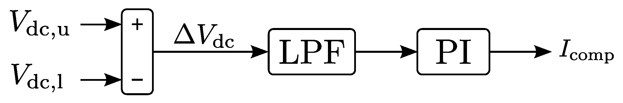
2.3. Mid-Point Balancing Techniques

To use the split-link converter, the influence of neutral-wire currents I n on the mid-point voltage must be actively compensated. The general idea of this compensation is to inject an additional compensating current I comp into the mid-point. There are two options for this injection.
The first option is to use the neutral wire and the grid itself for this compensating current, since it is already connected to the mid-point. The advantage is that the converter circuit is not altered. However, the compensating current will flow through the grid, which could be a disadvantage depending on the cause of the mid-point voltage unbalance. If the unbalance is caused by a dc component I n , dc , the compensating current would be opposite to this dc component and the amount of dc current injected into the grid through the neutral wire would reduce to zero. If the unbalance is caused by one of the ‘minor causes’, this method would increase the amount of dc current injected into the grid, although this current would be small in practice. The second option is to alter the converter circuit and inject the compensating current into the mid-point via an added conductor and an active balancing circuit. This increases the circuit complexity, and thus the cost. On the other hand, it brings more flexibility and functionality to the DG unit to provide power quality enhancement, as will be shown further in this article.
As an example of the first option, Zero-Sequence Current Injection (ZSCI) will be studied [15,16]. Another example of the first option is hysteresis band shifting of the current control [30,31]. This is only applicable if hysteresis controllers are used and has the same working principle as the aforementioned ZSCI method. Therefore, the hysteresis band shifting will not be considered in this article. As an example of the second option, the usage of a Half-Bridge Chopper (HBC) will be treated [10,17]. Another example of the second option is the use of two separate choppers, i.e., a boost and a buck chopper [32]. In [32], this has been used for a multi-level converter fed by a dc voltage source. Regarding the subject of this article, a two-level converter fed by a dc current source, this method would only result in an increased circuit complexity when compared to the HBC method. Therefore, it will not be considered further in this article as well.
Both ZSCI and HBC have been described in the literature. It is, however, not yet clear when which method is most appropriate. Also, detailed mathematical models have not been determined before in the discrete time domain. These models will be calculated in the Z domain here, which allows accurate design of the voltage control loops and implementation in digital control. Using simulations and experimental results, the advantages and disadvantages of each method will be clarified such that a sound choice between the two methods can be made in a practical application.

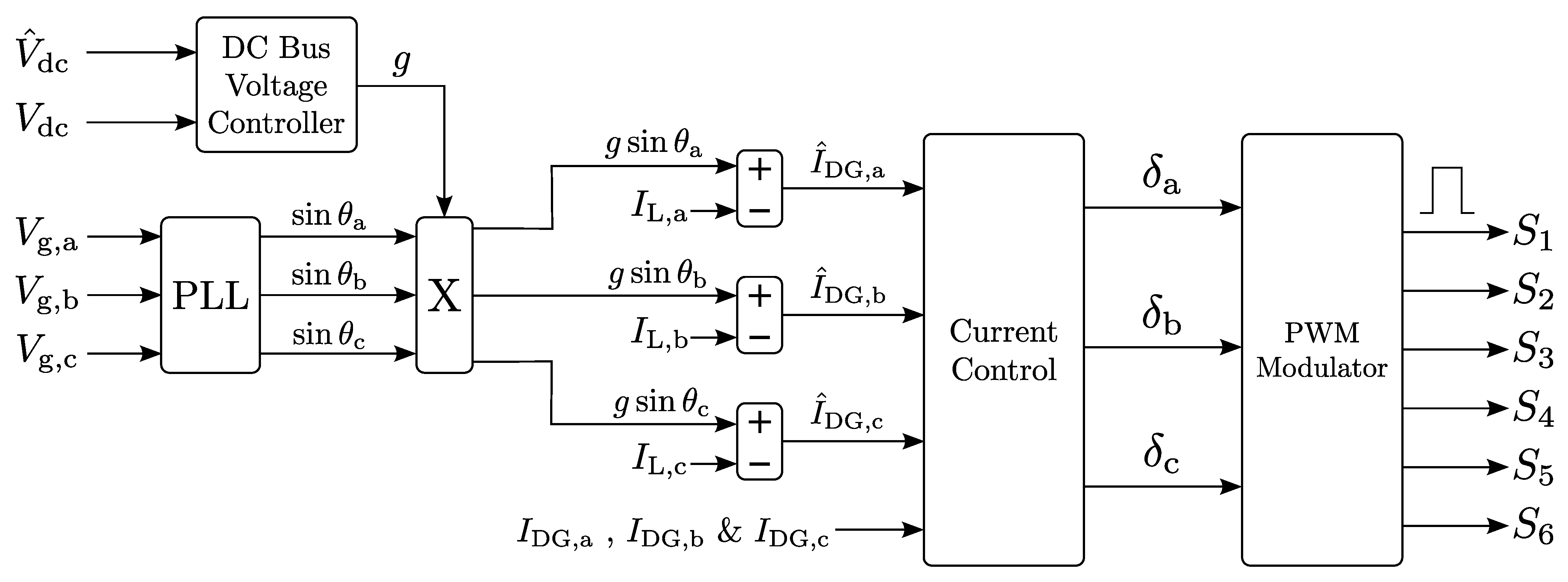
3. Zero-Sequence Current Injection

This section describes the ZSCI mid-point balancing technique. A discrete time domain model is derived which allows the tuning of the controller in the Z domain. This model is validated by means of a simulation model.

3.1. Description of the Technique

In Figure 3, it is shown that the duty ratio of each phase is determined by current control loops. These control loops ensure that the converter injects the desired currents and ac power into the grid. When the ZSCI method is used, a value I comp / 3 is added to the input of the current control loop of each phase. Hence, the converter will inject an additional zero-sequence current I comp / 3 into the grid. This will result in a returning current I comp in the neutral wire, influencing the voltage of the mid-point. The value of I comp is determined by the control scheme of Figure 6. The voltage unbalance Δ V dc is measured and filtered with a Low-Pass Filter (LPF) to leave only the low-frequent (mainly dc) component of Δ V dc . This serves as an input for the proportional-integral controller which calculates the compensating current I comp . In [15,16], a proportional controller was used in the control scheme. In the present article, a soft integral action is added to prevent a steady-state offset in Δ V dc .
The LPF is necessary to prevent the ZSCI method from compensating ac fluctuations in Δ V dc . This compensation would require that I n , ac is reduced to zero by the injection of I comp , which hinders most APF methods and is therefore undesired. The LPF does not prevent the ZSCI method from reducing I n , dc to zero. When using the ZSCI method, I n , dc must be reduced to zero to control the mid-point voltage. Therefore, this method does not allow dc currents in the neutral wire, although they could be desired by the APF method. Depending on the desired filtering functionality, this is a considerable drawback of ZSCI and limits the flexibility of the converter. Furthermore, the LPF reduces the reaction speed of the ZSCI method. On the other hand, the advantage of this method is that no additional components need to be added to the converter topology.

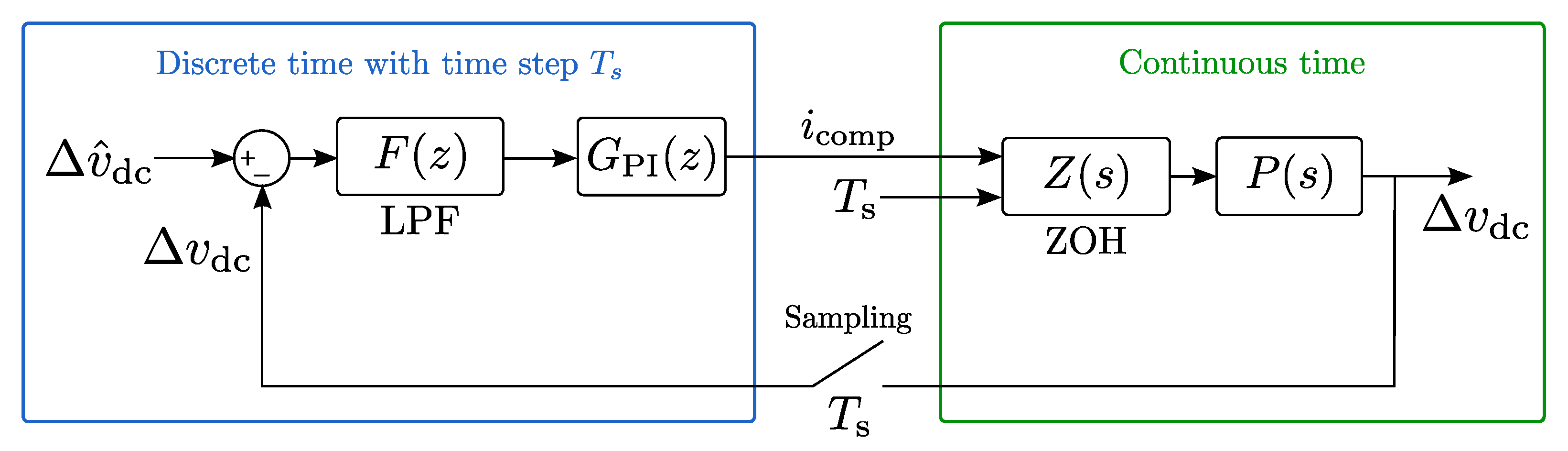
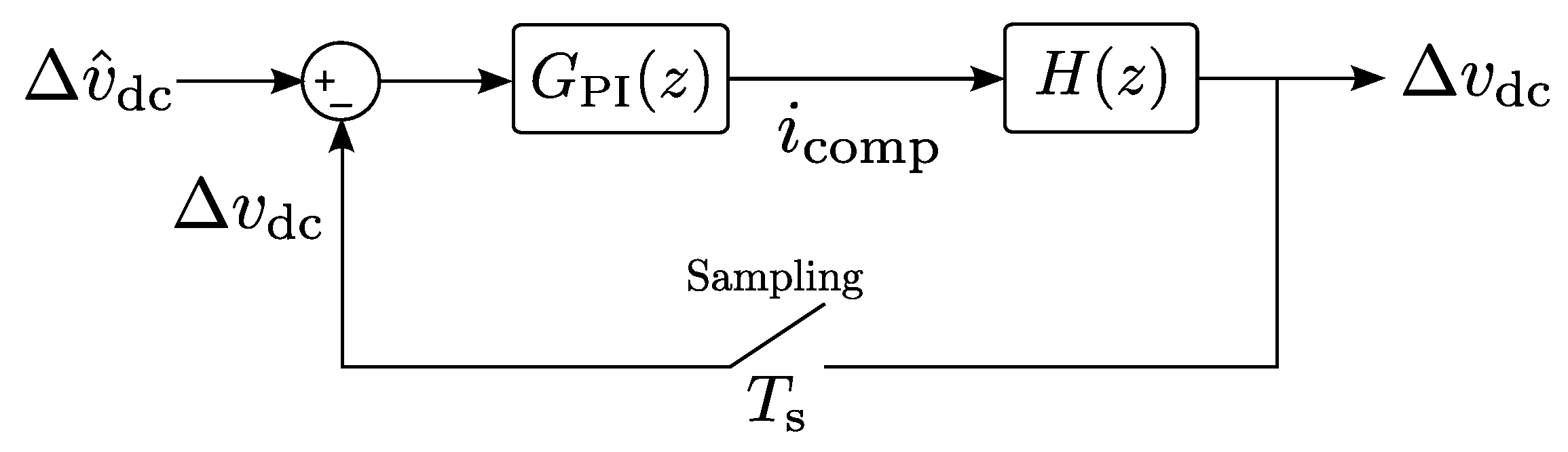
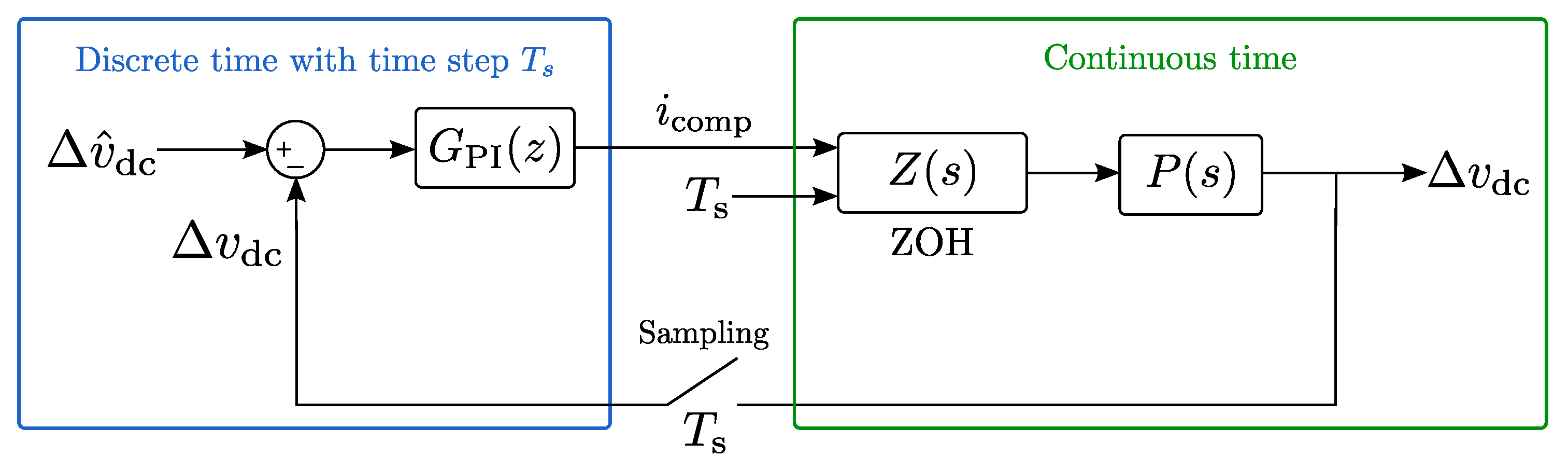
3.2. Discrete Time Domain Modeling

The ZSCI mid-point control method can be described in the discrete time domain by using the Z transformation and dimensionless parameters. When using digital control, a discrete time domain model of the system is more accurate than a classical Laplace domain representation, allowing a better control tuning. The dc bus voltage reference V dc , ref and current reference I ref are chosen as reference values for the dimensionless parameter system. Variables in relative quantities are written by using small letters.
Figure 7 shows the ZCSI method as a voltage control loop. The left part (blue) of the control loop is calculated in the digital discrete time domain with a time step T s . The right part (green) is the physical system in the continuous time domain. The control loop has a dimensionless voltage unbalance Δ v ^ dc = 0 as a set-point and Δ v dc as output. The control output I comp is then further regulated by a closed loop PI current controller, which is considerably faster than the mid-point voltage control. The voltage unbalance Δ v dc is calculated from the measurements of V dc , u and V dc , l obtained with a sampling period T s . The sampling period T s is chosen equal to the switching period of the converter because the sampling is synchronized to the PWM signals. The difference Δ v ^ dc Δ v dc is filtered by the first-order LPF with a cut-off pulsation ω c . The LPF transfer function F ( z ) in the discrete time domain is given by:
F ( z ) = A z + A z B
where A and B are defined as follows:
A = T s ω c 2 + T s ω c ; B = 2 T s ω c 2 + T s ω c
The PI controller is described by the transfer function G PI ( s ) in the Laplace domain and contains two parameters K p and K i :
G PI ( s ) = K p + K i s
For a digital implementation however, the PI controller should be written in the discrete time domain:
G PI ( z ) = K z a z 1
This representation of the controller can be derived from the Laplace-domain equation by application of the bilinear transformation or Tustin transformation. The result is a transfer function containing two parameters K and a. The output of the PI controller is the dimensionless compensating current i comp , which is used in the current control loops. The converter will inject this zero-sequence current into the grid, which will return via the neutral wire and will influence the mid-point voltage. This influence is described by the transfer function P ( s ) in the Laplace domain. Unlike the control, this is no longer a discrete time process, so a Zero-Order Hold (ZOH) is introduced in the control loop. The ZOH has the following transfer function Z ( s ) in the Laplace domain:
Z ( s ) = 1 exp ( s T s ) s
Equation (1) can be used to describe the influence of I comp on the mid-point voltage V dc , l :
I comp = 4 C dc d V dc , l d t
The total dc bus voltage V dc is assumed constant due to the bus voltage control loop as described in Section 2.2, and equal to the sum of V dc , u and V dc , l . The derivative of the voltage unbalance Δ V dc can be expressed as a function of the derivative of V dc , l :
d Δ V dc d t = d d t V dc , u V dc , l = d d t V dc 2 V dc , l = 2 d V dc , l d t
By using (8) and (9), the transfer function P ( s ) is calculated as:
P ( s ) = Δ v dc i comp = Δ V dc / V dc , ref I comp / I ref = I ref 2 C dc V dc , ref s = 1 τ s
The parameter τ = 2 C dc V dc , ref / I ref is the time constant of the integrating process. The transfer functions Z ( s ) and P ( s ) can be transformed to the Z domain together as follows:
Z { Z ( s ) · P ( s ) } = Z 1 exp ( s T s ) s · 1 τ s = T s τ 1 z 1
Combined with F ( z ) from (3), a new transfer function H ( z ) is introduced:
H ( z ) = F ( z ) · Z Z ( s ) · P ( s ) = T s τ A z + A ( z 1 ) ( z B )
By using H ( z ) , the control loop of Figure 7 can be simplified, which results in Figure 8. By using this simplified control scheme, the parameters K and a of the PI controller G PI ( z ) can be designed in the Z domain with classical Z domain control theory.

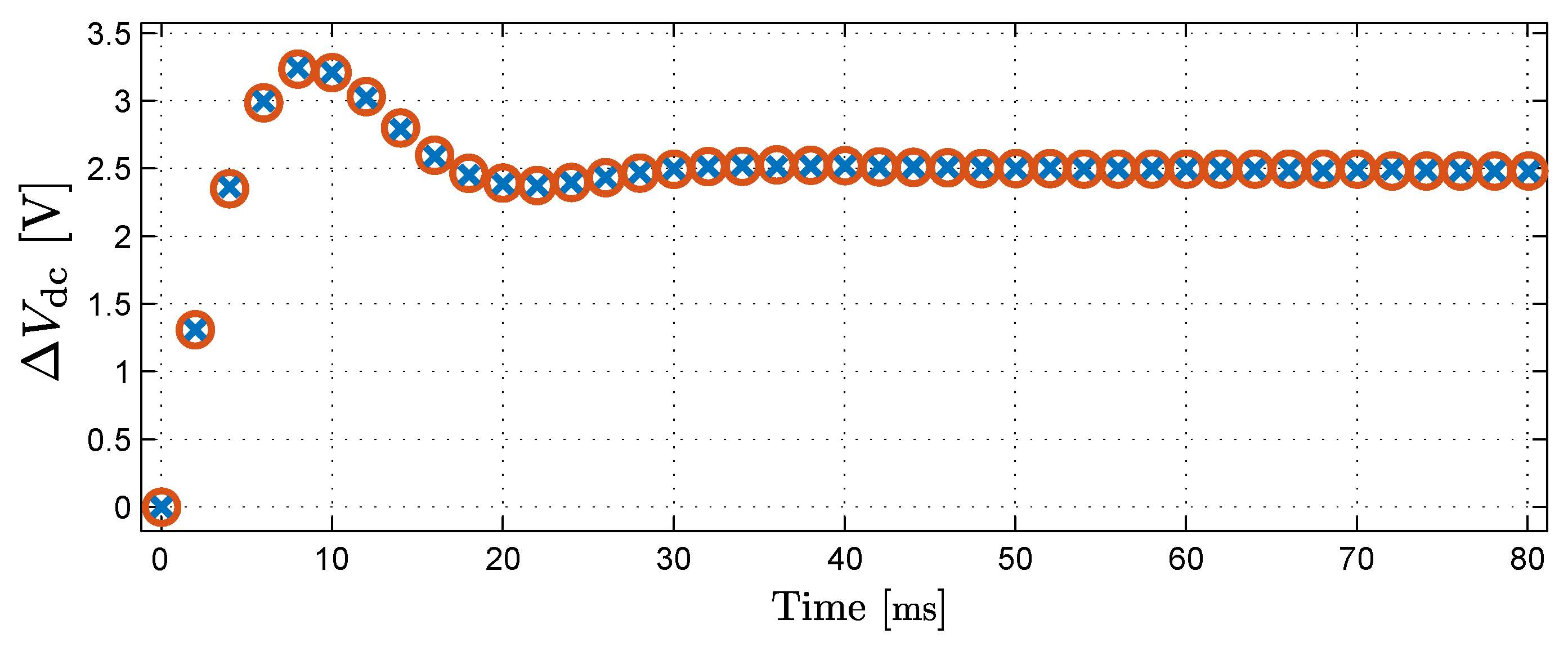
3.3. Simulation Results

The ZSCI method was implemented in the Matlab/Simulink simulation model of the split-link converter, as presented in Section 2. Table 3 shows the simulation parameters. The PI controller is designed by using Matlab SisoTool and H ( z ) (12), which results in:
G PI ( z ) = 1.65 z 0.99922 z 1
This controller has a bandwidth of 5 Hz and a phase margin of 37°. The bandwidth of 5 Hz is close to the bandwidth of the bus voltage controller, which should be sufficiently low to avoid fast power fluctuations at the converter output. To investigate the validity of the Z domain model of Figure 7, the step-responses of the simulation model and the Z domain model are compared. The set-point Δ V ^ dc receives a step from 0 V to 2.5 V. Figure 9 shows the result of this simulation. The circles represent the step-response from the simulation model, while the crosses represent the step-response from the Z domain model. It is clear that both step-responses have a good correspondence, which shows the validity of the Z domain model.
In the next simulation, the split-link converter was programmed as an APF, using the harmonic voltage damping technique [21,26]. The grid-voltage was distorted with a zero-sequence third harmonic of 10% of the rms value. Because of the used control strategy, the converter reacts by absorbing third harmonic currents to dampen the voltage harmonics through the voltage drop over the grid impedance. This third harmonic current causes a current in the neutral wire. The ZSCI should not interfere with this current, since it is a desired ac component, needed for the APF technique. The neutral-wire current causes a small ripple on the mid-point voltage, which is tolerated. In contrast, the ZSCI should react on a dc error of the mid-point voltage. To stress-test and verify the ZSCI control, a severe and sudden artificial current measurement error of −2 A in each phase is simulated at t = 0.3 s. This leads to a current of 2 A injected in each phase, −6 A in the neutral wire and a 1.5 kV/s increase of the mid-point voltage. The ZSCI should prevent the mid-point voltage from deviating from the 200 V set-point, by adjusting I comp to 6 A. The current measurement error is then compensated.
Figure 10 shows the result of this simulation. Before t = 0.3 s, there is no voltage unbalance and I comp is approximately zero. A small third harmonic is visible in Δ V dc due to the APF function. The sudden current measurement error occurs at t = 0.3 s. The voltage unbalance Δ V dc starts to decline, which causes the ZSCI to react by rising I comp . In steady state, the voltage unbalance Δ V dc restored to 0 V while I comp equals 6 A as predicted. This shows that the ZSCI can control the mid-point voltage during a severe disturbance.

4. Half-Bridge Chopper

This section describes the HBC mid-point balancing technique. Analogously to the previous section, a discrete time domain model is derived and validated by means of a simulation model.

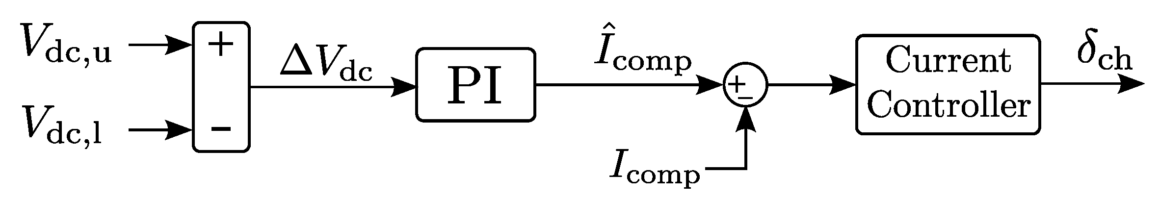
4.1. Description of the Technique

In the Half-Bridge Chopper (HBC) mid-point control method, the circuit is altered to inject the compensating current through an additional chopper, instead of using the neutral wire itself [10,17]. Similar active compensation circuits exist for other converter topologies, e.g., for half-bridge boost choppers [33]. Figure 11 shows the split-link converter topology with additional chopper circuit. The half-bridge chopper consists of the switches S 7 , S 8 and the inductor L ch . This chopper is controlled with a current control loop and injects the compensating current I comp into the mid-point. The set-point value of this current control loop is determined by the voltage unbalance Δ V dc .
Figure 12 shows the control scheme. The voltage unbalance Δ V dc is measured and sent directly to the PI voltage controller, which calculates the desired compensating current I ^ comp . The current controller then ensures that the chopper will deliver this current by regulating the duty ratio δ ch . A major difference between the ZSCI method and the HBC method is the absence of a Low-Pass Filter. This LPF is not required here because the HBC is not capable of interfering with APF functions. The advantage hereof is that the HBC can compensate ac fluctuations in Δ V dc (limited by the bandwidth of the voltage and current controller) as the HBC does not influence the currents that are injected into the grid by the converter.
Another difference between ZSCI and HBC is that the HBC method does not compensate dc currents in the neutral wire. If these dc currents are undesired, e.g., caused by current measurement errors, this is a disadvantage. However, if it is desired to inject dc currents into the grid by the used APF functions, the HBC method does not prevent this. Therefore, the HBC method offers more flexibility than the ZSCI method and allows the full use of APF functions such as the one described in Section 2.2. This may justify the higher cost of the converter.

4.2. Discrete Time Domain Modeling

Just like the ZSCI method, the HBC method can be described in the discrete time domain by using the Z transformation and dimensionless parameters. Figure 13 shows the voltage control loop, in which the left part (blue) is calculated in the digital discrete time domain with a time step T s while the right part (green) is the physical system in the continuous time domain. The only difference with the ZSCI control loop of Figure 7 is the absence of an LPF. Therefore, just like the ZSCI control loop, the HBC control loop can be simplified to Figure 8. Please note that again, the current control is sufficiently faster than the mid-point voltage control. The transfer function H ( z ) must be redefined as follows:
H ( z ) = Z Z ( s ) · P ( s ) = T s τ 1 z 1
By using this simplified control scheme and the new definition of H ( z ) , the parameters K and a of the PI controller G PI ( z ) can be designed in the Z domain with the classical control theory.

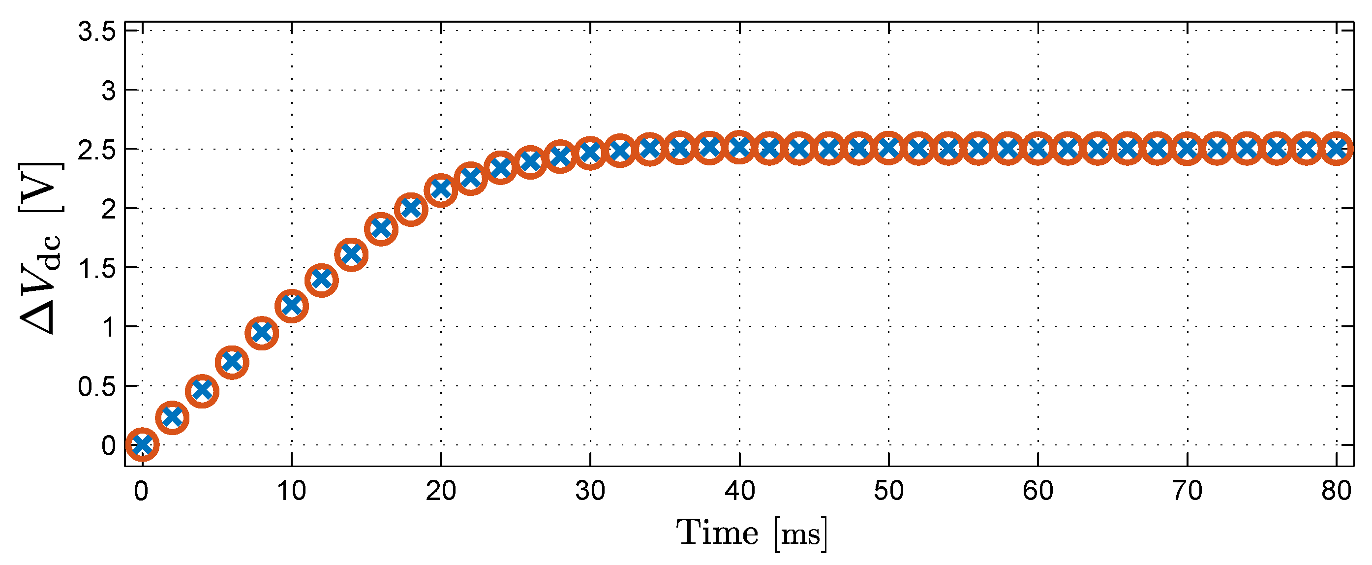
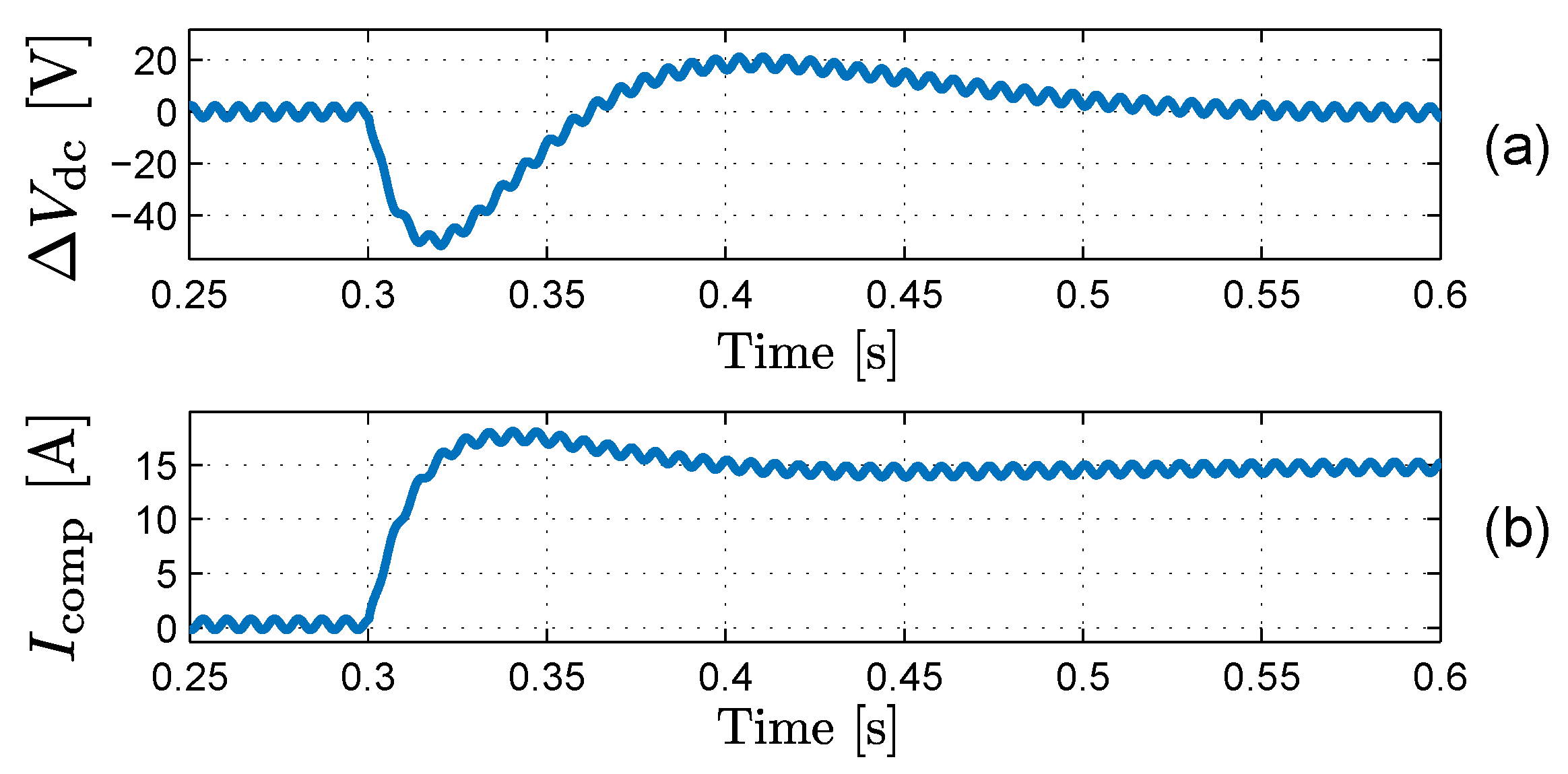
4.3. Simulation Results

The Half-Bridge Chopper was implemented in the simulation model with the same T s , C dc , I ref , V dc , ref and V dc values as for the ZSCI simulations in Section 3.3. The PI controller was designed as follows:
G PI ( z ) = 14 z 0.986 z 1
The controller has a bandwidth of 56 Hz and a phase margin of 51°. Compared with the PI controller of the ZSCI method given in Section 3.3, the bandwidth can be significantly higher because the HBC method does not use a LPF filter. This improves the reaction speed of the HBC method. To investigate the validity of the Z domain model of Figure 13, the step-responses of the simulation model and the Z domain model are compared. The set-point Δ V ^ dc receives a step from 0 V to 2.5 V. Figure 14 shows the result of this simulation. The circles represent the step-response from the simulation model, while the crosses represent the step-response from the Z domain model. Again, both step-responses have a good correspondence, which shows the validity of the model.
In the next simulation, the harmonic voltage damping technique [21] was used as an APF function. Figure 15 shows the result of this simulation. Again, the grid-voltage was distorted with a zero-sequence third harmonic of 10%. The converter will react by absorbing third harmonic currents, which are present in the neutral wire. These currents cause a small ripple on the mid-point voltage, which will be reduced by the HBC method by injecting an ac current into the mid-point, without interfering with the APF functionality (notice the scale of the figure). To verify the reaction of the HBC, a severe and sudden artificial current measurement error of −2 A in each phase is simulated. The HBC should prevent the mid-point voltage from deviating too much from 200 V, by adjusting I comp to 6 A, just like the ZSCI method did under the same circumstances.
The sudden current measurement error occurs at t = 0.3 s. The voltage unbalance Δ V dc starts to decline, which causes the HBC to react by rising I comp . In steady state, the voltage unbalance Δ V dc restored to 0 V while I comp meanly equals 6 A as predicted. Also, an ac component is present in I comp . The reason for this is that the HBC can compensate an ac component in Δ V dc . This simulation shows that the HBC can control the mid-point voltage during a severe disturbance.
A major difference with the ZSCI method is that the converter keeps injecting a dc current of 2 A into the grid in each phase. The neutral-wire current of 6 A is now diverted from the bus capacitors and bypassed through the chopper. This is in large contrast with the ZSCI method, where this neutral-wire current would be completely compensated. This compensation is desired in the case of a current measurement error but undesired when the dc current originates from an APF function.

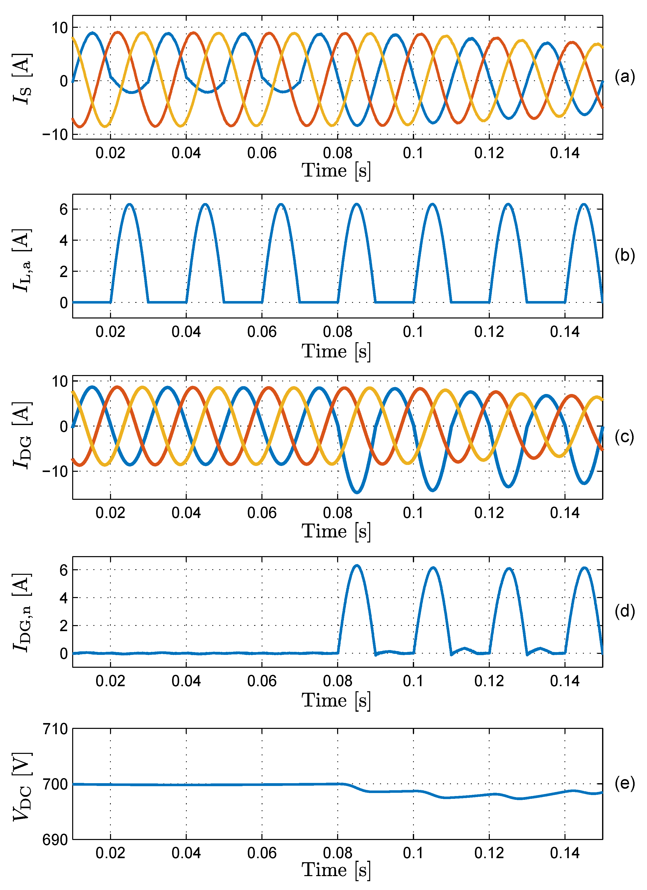
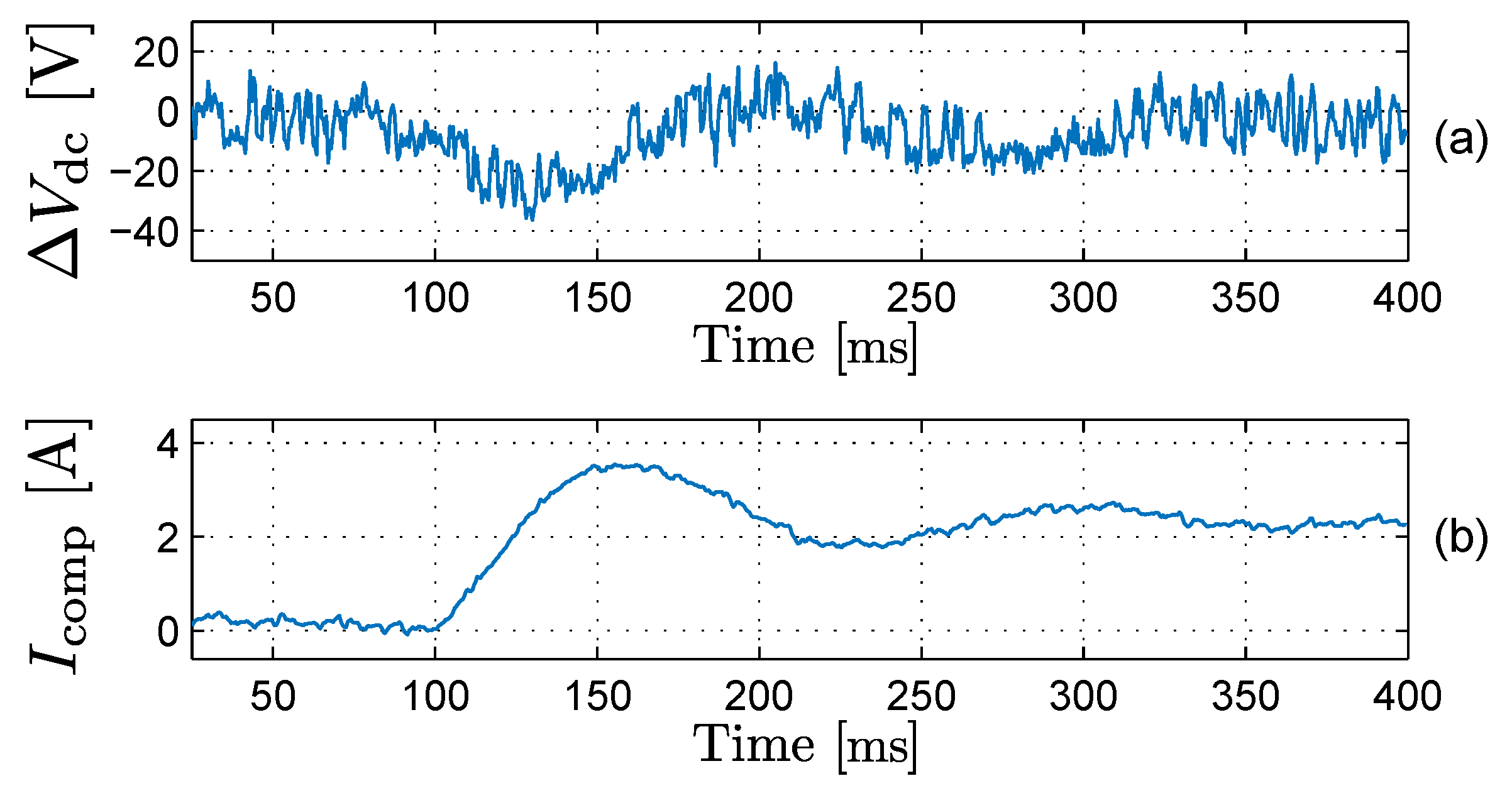
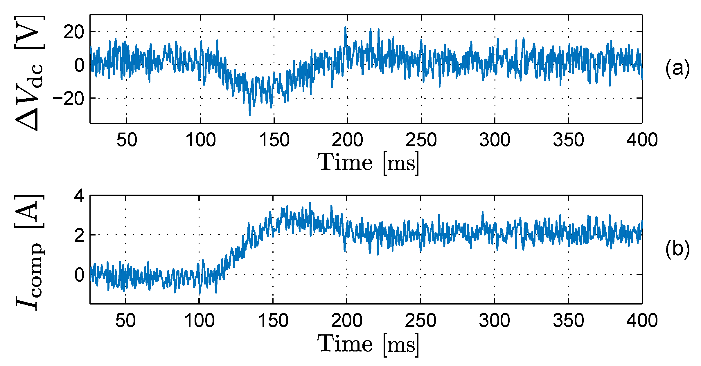
5. Experimental Validation

The ZSCI and HBC mid-point balancing techniques were experimentally validated on a laboratory split-link converter. Table 4 shows the values used for the test setup. The switches are IGBTs and the converter was controlled by a 16-bit 56F8367 Motorola DSP. The dc bus was powered by a Sorensen SGI600/17C, used as a current source. The grid-voltage was created with a Spitzenberger & Spies PAS15000 three-phase mains voltage simulator.

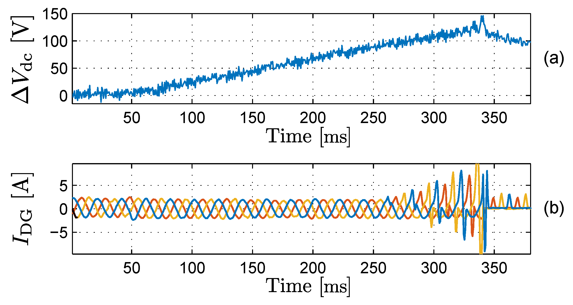
5.1. No Mid-Point Control

In the first measurement, the converter is injecting three-phase balanced sinusoidal currents into the grid, while no APF functions are enabled. In this situation, the only possible cause of neutral-wire currents are current measurement offsets. The current measurements were carefully calibrated before this test. Figure 16 shows the result of this experiment. Initially, the ZSCI method is used to control the mid-point. The mid-point voltage is well controlled, as the voltage unbalance Δ V dc is zero. At t = 50 ms, the ZSCI is disabled, causing the voltage unbalance Δ V dc to rise. The unbalance increases with a slope corresponding to a neutral-wire dc current of 50 mA, caused by small current measurement offsets. At first, the currents remain sinusoidal. At t = 255 ms however, the current control is no longer stable. At t = 345 ms, the converter shuts down and the IGBT’s stop receiving gate signals. The free-wheel diodes start conducting and the converter becomes a natural passive rectifier. This measurement shows that the mid-point control is absolutely necessary to use the split-link converter in practice. Even calibrated current measurements can cause a small dc current in the neutral wire which destabilizes the mid-point voltage rapidly.

5.2. Zero-Sequence Current Injection

The response of the ZSCI method is verified experimentally by introducing a sudden artificial current measurement offset error of −0.732 A in each phase at t = 100 ms. This results in an additional current of 0.732 A in each phase and a current of −2.196 A in the neutral wire. Just like in the simulation results presented in Section 3.3, the ZSCI method should regulate I comp to 2.196 A to compensate the current measurement error. Figure 17 shows the result of this measurement. The voltage unbalance Δ V dc rises at t = 100 ms but is quickly stabilized by the ZSCI. The compensating current I comp reaches 2.196 A in steady state, as predicted. This measurement shows that the ZSCI method succeeds in stabilizing the mid-point voltage in practice.

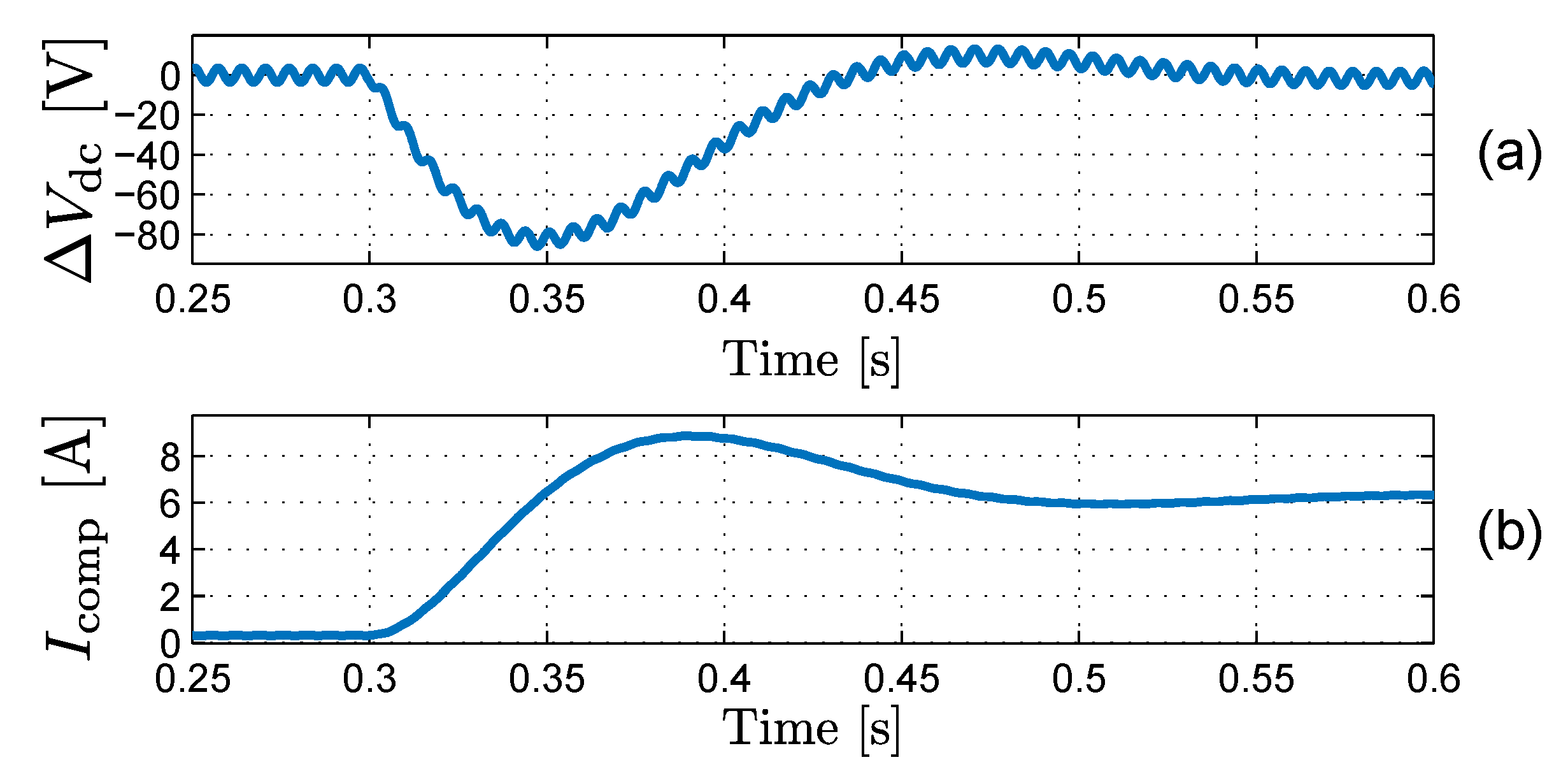
5.3. Half-Bridge Chopper

An identical experiment is performed to validate the HBC method. Figure 18 shows the result of this measurement. Again, at t = 100 ms, the voltage unbalance starts to rise due to the artificially introduced current measurement error. The chopper reacts by injecting current into the mid-point. In steady state, this current I comp reaches 2.196 A, as predicted. Just like the ZSCI method, the HBC method succeeds in stabilizing the mid-point voltage in practice. It should be noted that the HBC method reaches the steady-state condition faster than the ZSCI method. The reason for this is the LPF used for the ZSCI, as this LPF reduces the bandwidth of the voltage control loop.

6. Conclusions

In this article, the three-phase four-wire split-link converter is proposed as a multi-functional converter topology for smart DG units. By implementing an APF technique in the converter control, the power quality can be improved in a distributed manner. The split-link converter has a simpler topology and control compared to alternative topologies, e.g., the four-leg converter. However, the mid-point of the split dc bus capacitors must be actively balanced to ensure an equal voltage over both capacitors. Two balancing techniques, i.e., the injection of zero-sequence currents and the use of a half-bridge chopper have been analyzed and compared. For both, a discrete time domain model is derived which allows the design of the controllers for digital implementation. The techniques are validated with simulations and experiments.
The ZSCI technique requires no hardware adjustment to the converter topology. However, the converter is unable to inject dc currents into the grid, which is a drawback for certain APF techniques. The necessity of a low-pass filter in the control loop results in a reduction of the control bandwidth, leading to a slower response. However, for most applications the response of the ZSCI is sufficiently fast. Finally, ac fluctuations in Δ V dc cannot be compensated using ZSCI as this would require compensating ac currents passing through the grid, which is undesired and hinders the APF function. Therefore, the dc link capacitance should be sufficiently large to mitigate these ac fluctuations. The use of a half-bridge chopper increases the circuit complexity, and thus cost. However, it offers a few advantages, such as the capability to inject dc currents into the grid. This functionality is required by certain APF techniques, and makes the split-link converter equipped with a half-bridge chopper a more multi-functional topology. Moreover, the half-bridge chopper exhibits a faster response in mitigating mid-point voltage unbalances, as no low-pass filter is present in the control loop. Also, ac fluctuations in Δ V dc can be compensated, since the compensating currents do not have to pass through the grid, but are injected by the half-bridge chopper into the mid-point directly.

Author Contributions

Conceptualization, methodology, validation, investigation and writing, J.D.M.D.K.; review and editing, D.B. and L.V.; supervision, L.V.; All authors have read and agreed to the published version of the manuscript.

Funding

This research received no external funding.

Conflicts of Interest

The authors declare no conflict of interest.

References

  1. The International Renewable Energy Agency (IRENA). Renewable Energy Statistics; IRENA: Abu Dhabi, United Arab Emirates, 2020. [Google Scholar]
  2. Bozalakov, D.; Laveyne, J.; Mnati, M.J.; Van de Vyver, J.; Vandevelde, L. Possible power quality ancillary services in low voltage grids provided by the three-phase damping control strategy. Appl. Sci. 2020, 10, 7876. [Google Scholar] [CrossRef]
  3. Alotaibi, I.; Abido, M.A.; Khalid, M.; Savkin, A.V. A Comprehensive Review of Recent Advances in Smart Grids: A Sustainable Future with Renewable Energy Resources. Energies 2020, 13, 6269. [Google Scholar] [CrossRef]
  4. Bozalakov, D.; Vandoorn, T.; Meersman, B.; Papagiannis, G.; Chrysochos, A.; Vandevelde, L. Damping-based droop control strategy allowing an increased penetration of renewable energy resources in low voltage grids. IEEE Trans. Power Deliv. 2016, 31, 1447–1455. [Google Scholar] [CrossRef]
  5. Chaoui, A.; Gaubert, J.P.; Krim, F.; Champenois, G. PI controlled three-phase shunt active power filter for power quality improvement. Electr. Power Components Syst. 2007, 35, 1331–1344. [Google Scholar] [CrossRef]
  6. Bozalakov, D.; Laveyne, J.; Desmet, J.; Vandevelde, L. Overvoltage and voltage unbalance mitigation in areas with high penetration of renewable energy resources by using the modified three-phase damping control strategy. Electr. Power Syst. Res. 2019, 168, 283–294. [Google Scholar] [CrossRef]
  7. Sun, X.; Han, R.; Shen, H.; Wang, B.; Lu, Z.; Chen, Z. A double-resistive active power filter system to attenuate harmonic voltages of a radial power distribution feeder. IEEE Trans. Power Electron. 2016, 31, 6203–6216. [Google Scholar] [CrossRef]
  8. Manandhar, U.; Zhang, X.; Gooi, H.B.; Wang, B.; Fan, F. Active DC-link balancing and voltage regulation using a three-level converter for split-link four-wire system. IET Power Electron. 2020, 13, 2424–2431. [Google Scholar] [CrossRef]
  9. De Kooning, J.D.M.; Meersman, B.; Vandoorn, T.; Renders, B.; Vandevelde, L. Comparison of three-phase four-wire converters for distributed generation. In Proceedings of the International Universities Power Engineering Conference (UPEC2010), Cardiff, UK, 31 August–3 September 2010. [Google Scholar]
  10. Liang, J.; Green, T.C.; Feng, C.; Weiss, G. Increasing Voltage Utilization in Split-Link, Four-Wire Inverters. IEEE Trans. Power Electron. 2009, 24, 1562–1569. [Google Scholar] [CrossRef] [Green Version]
  11. Zhang, R.; Prasad, V.H.; Boroyevich, D.; Lee, F.C. Three-Dimensional Space Vector Modulation for Four-Leg Voltage-Source Converters. IEEE Trans. Power Electron. 2002, 17, 314–326. [Google Scholar] [CrossRef]
  12. Bifaretti, S.; Lidozzi, A.; Solero, L.; Crescimbini, F. Modulation with sinusoidal third-harmonic injection for active split DC-bus four-leg inverters. IEEE Trans. Power Electron. 2016, 31, 6226–6236. [Google Scholar] [CrossRef]
  13. Urrea-Quintero, J.-H.; Muñez-Galeano, N.; López-Lezama, J.M. Robust Control of Shunt Active Power Filters: A Dynamical Model-Based Approach with Verified Controllability. Energies 2020, 13, 6253. [Google Scholar] [CrossRef]
  14. Hammami, M.; Mandrioli, R.; Viatkin, A.; Ricco, M.; Grandi, G. Analysis of Input Voltage Switching Ripple in Three-Phase Four-Wire Split Capacitor PWM Inverters. Energies 2020, 13, 5076. [Google Scholar] [CrossRef]
  15. Seguí-chilet, S.; Gimeno-sales, F.J.; Orts, S.; Alcañiz, M.; Masot, R. Selective shunt active power compensator in four wire electrical systems using symmetrical components. Electr. Power Components Syst. 2006, 35, 97–118. [Google Scholar] [CrossRef]
  16. Casaravilla, G.; Eirea, G.; Barbat, G.; Inda, J.; Chiaramello, F. Selective active filtering for four-wire loads: Control and balance of split capacitor voltages. In Proceedings of the PESC 2008: 39th IEEE Annual Power Electronics Specialists Conference, Rhodes, Greece, 15–19 June 2008; pp. 4636–4642. [Google Scholar]
  17. Mishra, M.K.; Joshi, A.; Ghosh, A. Control schemes for equalization of capacitor voltages in neutral clamped shunt compensator. IEEE Trans. Power Deliv. 2003, 18, 538–544. [Google Scholar] [CrossRef] [Green Version]
  18. Liu, Y.; Heydt, G.T.; Chu, R.F. The Power Quality Impact of Cycloconverter Control Strategies. IEEE Trans. Power Deliv. 2005, 20, 1711–1718. [Google Scholar] [CrossRef]
  19. Salas, V.; Alonso-Abella, M.; Olías, E.; Chenlo, F.; Barrado, A. DC Current Injection into the Network from PV inverters of <5 kW for Low-Voltage Small Grid-Connected PV Systems. Sol. Energy Mater. Sol. Cells 2007, 91, 801–806. [Google Scholar]
  20. Chung, S.-K. A Phase Tracking System for Three Phase Utility Interface Inverters. IEEE Trans. Power Electron. 2000, 15, 431–438. [Google Scholar] [CrossRef] [Green Version]
  21. Renders, B.; Gussemé, K.D.; Ryckaert, W.R.; Vandevelde, L. Converter-connected distributed generation units with integrated harmonic voltage damping and harmonic current compensation function. Electr. Power Syst. Res. 2009, 79, 65–70. [Google Scholar] [CrossRef]
  22. Green, T.C.; Marks, J.H. Control Techniques for active power filters. IEE Proc. Electr. Power Appl. 2005, 152, 369–381. [Google Scholar] [CrossRef] [Green Version]
  23. Singh, B.; Al-Haddad, K.; Chandra, A. Harmonic elimination, reactive power compensation and load balancing in three-phase, four-wire electric distribution systems supplying non-linear loads. Electr. Power Syst. Res. 1998, 44, 93–100. [Google Scholar] [CrossRef]
  24. Rao, U.K.; Mishra, M.K.; Ghosh, A. Control Strategies for Load Compensation Using Instantaneous Symmetrical Component Theory Under Different Supply Voltages. IEEE Trans. Power Deliv. 2008, 23, 2310–2317. [Google Scholar] [CrossRef]
  25. Antchev, M.H. Classical and Recent Aspects of Active Power Filters for Power Quality Improvement. In Classical and Recent Aspects of Power System Optimization; Zobaa, A.F., Aleem, S.A., Abdelaziz, A.Y., Eds.; Academic Press: London, UK, 2018; Chapter 9. [Google Scholar]
  26. Núñez-Zúñiga, T.E.; Pomilio, J.A. Shunt Active Power Filter Synthesizing Resistive Loads. IEEE Trans. Power Electron. 2002, 17, 273–278. [Google Scholar] [CrossRef]
  27. Akagi, H.; Kanazawa, Y.; Nabae, A. Instantaneous reactive power compensators comprising switching devices without energy storage components. IEEE Trans. Ind. Appl. 1984, IA-20, 625–630. [Google Scholar] [CrossRef]
  28. Montero, M.I.M.; Cadaval, E.R.; González, F.B. Comparison of Control Strategies for Shunt Active Power Filters in Three-Phase Four-Wire Systems. IEEE Trans. Power Electron. 2007, 22, 229–236. [Google Scholar] [CrossRef]
  29. Czarnecki, L.S. Comments on measurement and compensation of fictitious power under non-sinusoïdal voltage and current conditions. IEEE Trans. Power Electron. 1990, 5, 503–504. [Google Scholar] [CrossRef]
  30. Lafoz, M.; Iglesias, I.J.; Veganzones, C.; Visiers, M. A Novel Double Hysteresis-Band Current Control for a Three-Level Voltage Source Inverter. In Proceedings of the PESC 2000: 31th IEEE Annual Power Electronics Specialists Conference, Galway, Ireland, 18–23 June 2000; pp. 21–26. [Google Scholar]
  31. Aredes, M.; Heumann, K.; Watanabe, E.H. An universal active power line conditioner. IEEE Trans. Power Deliv. 1998, 13, 545–551. [Google Scholar] [CrossRef]
  32. von Jouanne, A.; Dai, S.; Zhang, H. A Multilevel Inverter Approach Providing DC-Link Balancing, Ride-Through Enhancement, and Common-Mode Voltage Elimination. IEEE Trans. Ind. Electron. 2002, 49, 739–745. [Google Scholar] [CrossRef]
  33. Bayona, J.; Gélvez, N.; Espitia, H. Design, Analysis, and Implementation of an Equalizer Circuit for the Elimination of Voltage Imbalance in a Half-Bridge Boost Converter with Power Factor Correction. Electronics 2020, 9, 2171. [Google Scholar] [CrossRef]
Figure 1. Four-leg (top) and split-link (bottom) converter topologies.
Electronics 10 00506 g001
Figure 2. Distribution feeder with resistive load, DG unit and non-linear load.
Electronics 10 00506 g002
Figure 3. Converter control scheme.
Electronics 10 00506 g003
Figure 4. Phase-Locked Loop (PLL) schematic.
Electronics 10 00506 g004
Figure 5. Distribution grid simulation results: (a) source currents I S , (b) load current I L , a , (c) DG-unit currents I DG , (d) DG-unit neutral-wire current I n , (e) DG-unit dc bus voltage V dc . Three-phase currents are denoted in blue, yellow and orange.
Electronics 10 00506 g005
Figure 6. Zero-sequence Current Injection control scheme.
Electronics 10 00506 g006
Figure 7. Zero-sequence Current Injection control loop.
Electronics 10 00506 g007
Figure 8. Zero-Sequence Current Injection simplified control scheme.
Electronics 10 00506 g008
Figure 9. Zero-Sequence Current Injection step-response (simulation). Circles: simulation model, Crosses: Z domain model.
Electronics 10 00506 g009
Figure 10. Simulated effect of an artificial current measurement error on the ZSCI control: (a) Voltage unbalance Δ V dc , (b) Compensating current I comp .
Electronics 10 00506 g010
Figure 11. Split-link converter with half-bridge chopper as an active mid-point balancing circuit.
Electronics 10 00506 g011
Figure 12. Half-Bridge Chopper control scheme.
Electronics 10 00506 g012
Figure 13. Half-Bridge Chopper control loop.
Electronics 10 00506 g013
Figure 14. Half-Bridge Chopper step-response (simulation). Circles: simulation model, Crosses: Z domain model.
Electronics 10 00506 g014
Figure 15. Effect of an artificial current measurement error on the HBC control: (a) Voltage unbalance Δ V dc , (b) Compensating current I comp .
Electronics 10 00506 g015
Figure 16. Disabling mid-point control at t = 50 ms (experimental): (a) voltage unbalance Δ V dc , (b) DG-unit three-phase currents I DG in blue, yellow and orange.
Electronics 10 00506 g016
Figure 17. Effect of a current measurement error on ZSCI on t = 100 ms (experimental): (a) Voltage unbalance Δ V dc , (b) Compensating current I comp .
Electronics 10 00506 g017
Figure 18. Effect of a current measurement error on HBC on t = 100 ms (experimental): (a) Voltage unbalance Δ V dc , (b) Compensating current I comp .
Electronics 10 00506 g018
Table 1. Split-link converter parameters.
f switch C dc I ref V dc L f C f
20 kHz10 mF25 A700 V2 mH5 µF
Table 2. BAXB cable parameters.
R a , b , c R n L R a , b , c /X I nom
0.410 Ω/km0.713 Ω/km0.243 mH/km5.37255 A
Table 3. Simulation parameters.
ω c T s C dc I ref V dc , ref V dc
2 π 10 Hz 50 µ s 1 mF 24 A 600 V 400 V
Table 4. Test-setup values.
T s C dc V dc L f and L ch C f V grid
50 µs1 mF400 V2.1 mH5 µF115 V
Publisher’s Note: MDPI stays neutral with regard to jurisdictional claims in published maps and institutional affiliations.

