1. Introduction
Nowadays, urban environments are saturated with electromagnetic energy produced by the wireless devices used in our daily routines. This energy is meant for limited numbers of people, but everyone is exposed to it. Apart from causing interferences for nearby devices, it may also has adverse long-term effects on human health, causing tissue damage as well as the development of tumors in the worst cases [
1,
2,
3,
4,
5]. In secured installations, such as intensive care units (ICUs), security and military installations, operation theaters, and cardiac care units (CCUs), communication can be restricted to frequency spectra below the C-band (4 GHz–8 GHz), in which only 3G and 4G mobile connectivity is maintained. This limitation very much suffices for basic communication needs. In these systems, all higher-frequency signals, such as those in the upper 802.11ac WLAN band, as well as in some ISM bands, are desired to be rejected.
In addition, the X-band (8–12 GHz) (used in space communications and radars) is another high-frequency and high-power electromagnetic (EM) spectrum that is present in the environment and can endanger human beings. The mitigation of RF radiation in restricted zones where security is a prime concern is often required by security agencies. Therefore, to mitigate unwanted EM radiation and electromagnetic interference (EMI) in controlled environments, several methods have been practiced, such as shielding an environment/device using metal foils or metallic coating [
6]. These conventional shielding methods block useful signals along with unwanted signals, and also add additional cost, weight, and bulkiness to devices [
6,
7].
On the contrary, frequency-selective surfaces (FSSs) [
8], due to their single- and multi-band frequency suppression characteristics, have been extensively used in military installations, secure locations such as jails, and various other sites [
9,
10]. In the literature, several configurations of FSSs have been reported to mitigate EMI for GSM, WLAN/Wi-Fi, and X-band signals in a single- or multi-mode operation [
11,
12,
13]. In addition, frequency-reconfigurable and tunable FSSs that are capable of shielding more than two frequency bands have also been reported [
14,
15,
16,
17,
18]. Various methods, such as mechanical deformation, material tuning, circuit biasing, and micro-fluidic techniques, have been employed to alter the frequency response of FSSs [
19]. However, mechanical deformations are difficult to implement due to complexities related to their physical controls. Similarly, material tuning causes surfaces to suffer from environmental conditions, such as humidity and changes in temperature. Circuit biasing is a frequently employed method for achieving reconfiguration. Varactor and PIN diodes have been used [
7,
11,
12]. The active shields realized using the above-mentioned techniques are extremely useful in extracting the optimal frequency spectra as per the requirements of end users. Nonetheless, the major limitations associated with these active FSSs are their polarization dependence and poor shielding performance at different angles of incidence [
14,
15,
16].
The authors of [
16] proposed a Jerusalem-cross-based tunable FSS with a unit cell size of 27.5 mm to shield 900 and 1800 MHz, whereas varactors were used to tune lower bands. However, the authors did not report the FSS’s behavior for transverse electric (TE), transverse magnetic (TM) polarizations, or the shielding stability at normal and oblique incidence angles. In addition, a tunable meta-material FSS with 10.5 mm size was tuned from 3 to 3.5 GHz band by using varactors on both sides of the substrates [
17], but polarization independence of the FSS was not established to demonstrate its suitable candidacy for practical applications. An FSS geometry with a unit cell size of 10.5 mm operating at 5.8 GHz was made reconfigurable by using a mechanical setup that altered the gaps between the FSS elements in order to attain frequency-reconfigurable operation [
18]. Nevertheless, the performance of the FSS proposed in [
18] at oblique incidence angles was not reported. In addition, reconfigurable FSSs using two techniques—one was based on using diodes to change the current distribution, and the second was based on mechanical rotation of the FSS—were proposed in [
20]. The realizations of both techniques were performed only in simulations, which, therefore, may raise performance concerns in the practical realization of the proposed FSS shields. In [
21], a venetian-blind-based shutter mechanism was used to achieve reconfigurability in an FSS, but the shutter mechanism was employed manually. Similarly, a reconfigurable dual-band-stop FSS using a liquid crystal polymer was proposed in [
22] without in-depth analysis or discussions on the practical realization or angular stability. In the existing literature, only one flexible and reconfigurable FSS with angular stability has been proposed so far, which can be found in [
23]. The FSS proposed in [
23] was designed on flexible plastic and fabricated using an additive manufacturing process, whereas varactor diodes with a bias line on the same layer of the FSS were used to achieve frequency reconfigurability. The reported FSS offered better shielding performance by virtue of the costly additive manufacturing process, and it required extra effort to place the FSS on the host dielectric, which caused additional design bulkiness. In addition, the effect of strong coupling between RF and DC currents because of the placement of the FSS and DC bias lines on the same layers resulted in a poor shielding performance by the FSS.
It can be seen in the above literature review and discussion that, presently, FSS geometries with reconfigurability have sizes of about 2.7
or more for X-band shielding [
12], which is mainly because the multi-band, tunable, and reconfigurable shielding operations increase the size of the structure, and it is very hard to sustain the polarization independence and angular stability, as reported in the literature [
14,
15,
16,
17,
18]. In this very context, the objective of this work is to propose a highly compact and efficient FSS shield for X-band applications with an option of switching to C-band suppression. The novelty is justified because such compact FSS designs for switchable X- and C-band shielding are not available in the literature. In this paper, it is successfully demonstrated that the proposed FSS design has a stable frequency response for both the TE/TM and 45° polarizations at normal and oblique angles of incidence of up to 60°. The remainder of the paper is organized as follows: The FSS unit cell modeling and simulation results are presented in
Section 2. Mathematical and equivalent circuit models of the design are presented in
Section 3, whereas a parametric analysis of the design is discussed in
Section 4. The proposed mechanism of active switching to the C-band is discussed in
Section 5. A comparison of the simulated and measured results for various incident angles is shown in
Section 6, followed by the conclusion in the last section.
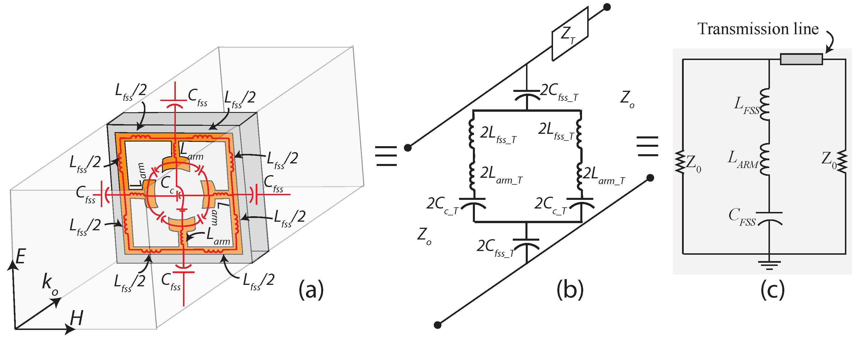
2. Proposed Passive FSS Unit Cell
A schematic view of the proposed square-loop FSS with inward-extended quarter-circular arms and with optimized dimensions is shown in
Figure 1a. The proposed design was realized on a single layer of a low-cost FR4 laminate with a thickness h = 1.6 mm, relative permittivity
= 4.4, and loss tangent tan
= 0.02. An FSS unit cell was first modeled and optimized in a 3D full-wave EM simulator (Ansys HFSS) [
24]. Initially, a conventional square loop was simulated, and its frequency response was observed. Afterwards, to miniaturize the proposed design and increase the angular stability of the proposed FSS, inward-extended quarter-circular arms were incorporated to achieve the maximum shielding effectiveness (SE) in the desired band. Furthermore, an inward-extended and curved arm was introduced to tune the shielding frequency by keeping the overall unit cell size at 4.8 mm × 4.8 mm. For the idealization of the FSS unit cell as an EM shield with infinite periodicity in the
x- and
y-axes, a Floquet port analysis [
25] with master and slave boundaries (linked boundaries) was performed to achieve the desired shielding effectiveness for the X-band. An illustration of the Floquet analysis along with the port declaration and periodic boundary setup is presented in
Figure 1b–d. Fundamentally, the Floquet modes impinge on an EM plane wave normal to the FSS, i.e., the propagation direction is set by the frequency, phasing, and geometry of the periodic structure. The simulator solution included a model decomposition with information on the performance of the radiating structure. The impinging EM waves in the Floquet modes then interrelated with the S-matrix, and the S-parameter results were computed for an infinite array under periodic boundary conditions (shown in
Figure 1b–d). Next, the dB value of
was plotted against the frequency to observe the SE of the designed FSS. The SE is often defined as the ratio of forward power transmitted by the source (
) to power received at the termination (
). Mathematically,
which can be further simplified and interpreted in terms of
as:
3. Equivalent Circuit Model (ECM)
To accurately predict the resonance behavior and SE of the proposed FSS, an equivalent circuit model (ECM) was extracted using the lumped element model theory [
26,
27,
28,
29,
30,
31], and the values were determined using the coupled-line theory [
26,
27]. A plane wave from port 1 (shown in
Figure 1b) propagates through free space and illuminates the shield. This illumination results in surface currents at the resonant frequency around the closed loop of the FSS [
27]. The free-space impedance is modeled as Z
(377
), whereas the square-loop conducting structure in the proposed FSS unit cell is modeled using inductances. For the symmetrical modeling, inductance is divided into half on both sides of the inner arms, which divide each leg of the square loop into two parts, as shown in
Figure 2a. The conductive nature of the inward-extended arms is also modeled as an inductor
, whereas the coupling capacitance
is incorporated to attribute the coupling between the inner extended arms. The construction and mapping of each conducting strip of the proposed FSS on the equivalent lumped elements are depicted in
Figure 2a. In addition,
in the lumped model is included to represent the coupling between the adjacent cells in a periodic structure of the proposed FSS. Since the distance between the inner extended arms is greater than the distance between the adjacent cells, the combined coupling capacitance
can be neglected during the subsequent circuit simplification (
Figure 2c). An illustration of the lumped element model extracted from
Figure 2a is depicted in
Figure 2b. The impedance of the dielectric used in the unit cell is modeled by
; however, it may be neglected because of the incomparable thickness of the substrate [
27].
It can be seen in
Figure 2c that the total impedance of the proposed FSS (Z
) is a series and parallel combination of the inductances and capacitances shown in
Figure 2b. Therefore, after simplification, the final construction of the ECM of the proposed FSS is effectively a series LC circuit in parallel with the free-space impedance at both ends. Mathematically, the FSS impedance Z
is expressed as [
26,
27]:
where
is the reactance corresponding to the complete length of the square loop.
represents the coupling between the two adjacent unit cells, and
represents the lengths of the inner extended arms, as shown in
Figure 2c. By replacing the equations for the reactances in Equation (
3), we get:
Rearranging Equation (
4),we obtain
Further simplification of Equation (
5) results in Equation (
6):
The shielding frequency
of the ECM in Equation (
6) is obtained by equating the numerator to zero [
29]. This implies that
It can be interpreted from Equations (6) and (7) that the combined capacitive and inductive reactances corresponding to the distance between adjacent unit cells and conductive strips of the FSS, respectively, cancel each other at the shielding frequency
. The cancellation of the inductive and capacitive reactances results in a short circuit in the ECM and, consequently, reflects all EM energy that strikes the surface of the shield. In addition, for
f <
, the capacitive nature of the lumped LC circuit dominates the resonance mechanism. Conversely, when the impedance of the series LC circuit is inductive at
f >
, a higher shielding frequency
with dominant inductive impedance—as compared to the capacitive impedance of the lumped LC circuit—results. Equation (
7) also shows that various combinations can be formulated using different values of inductances and capacitances through the lumped circuit theory [
27]. Therefore, for the shielding frequency of 11 GHz, when optimized through 3D EM simulations, the values of the equivalent lumped elements are finalized at
= 0.065 pF,
= 2.4 nH, and
= 0.8 nH. For the verification of the ECM, values of the reactances obtained from Equation (
7) were used to simulate
Figure 2c in a circuit simulator [
32]. A comparison between the SE of the unit cell modeled in the 3D EM software (
Figure 1) and the ECM is presented in
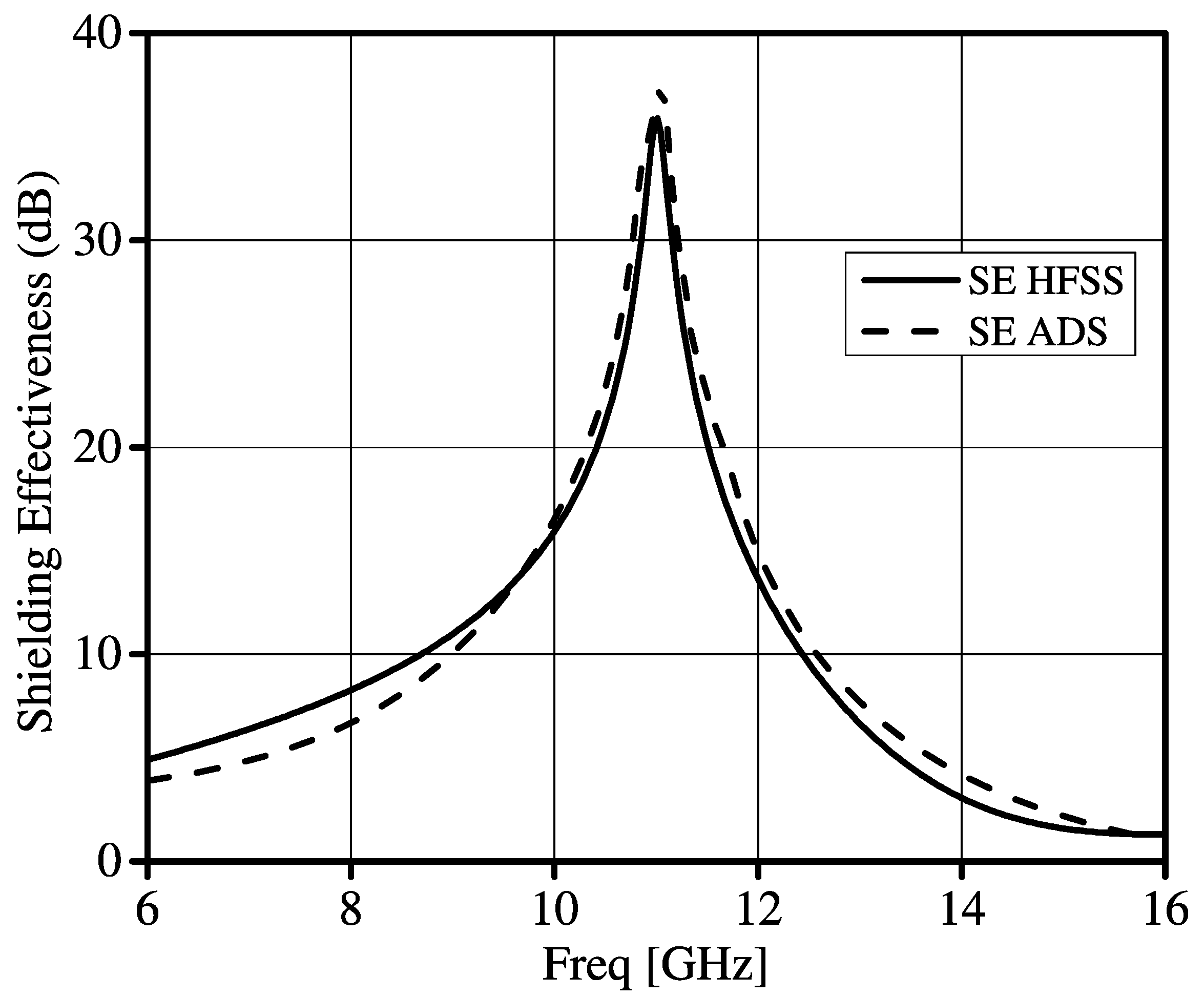
Figure 3. It shows that the EM simulation results are in good agreement with the circuit simulation results.
4. Parametric Analysis
After the simulation and circuit modeling of the unit cell, a detailed parametric analysis was performed to observe the behavior of the proposed FSS with variations in the geometric parameters and dielectric constant of the substrate. Specifically, variations in the shielding frequency were investigated by varying (1) unit element size, (2) the extended arm length
l, (3) the trace width
w of the unit element (shown in
Figure 1a), and (4) the dielectric constant
of the substrate. It was observed that changing the FSS parameters altered the overall inductance
and capacitance
of the FSS structure. Mathematically, inductance is expressed as [
31]:
where
is the permeability of free space,
l is the length of inner extended arms of the FSS unit cell,
D is the overall length of the square loop, and
w is the width of the FSS conductor. Equation (
8) shows that inductance
has direct dependence on D, whereas an increase in width
w decreases the inductance of the FSS structure. The direct and indirect dependence of the length and width of the FSS was verified by performing a parametric analysis on the length and width of the FSS unit cell in the EM simulator.
Figure 4a shows the effect on shielding frequency with respect to the change in FSS length. It can be seen in
Figure 4a that changing the arm length while keeping other parameters constant shifts the shielding frequency of the proposed FSS. Similarly, performing a parametric analysis on the width
w of the FSS unit cell showed that inductance decreases as
w increases; thus, shielding frequency shifts to the higher side, as shown in
Figure 4b. Furthermore, the effect on the shielding frequency
was observed by changing inter-element spacing
r. It was observed that an increase in
r decreases the capacitance of the FSS units and results in a higher shielding frequency, as is evident in
Figure 4c and the relation given in Equation (
9).
The dielectric constant
was also varied to analyze the FSS’s performance, and the corresponding results are shown in
Figure 4d. It was observed that, as the value of
starts increasing, the
tends to decrease. This is because the square-loop length
D is inversely related to
; mathematically, it is represented as [
12]:
where
is the effective permittivity and is approximated as
.
Angular Stability of the FSS at Normal and Oblique Angles of Incidence
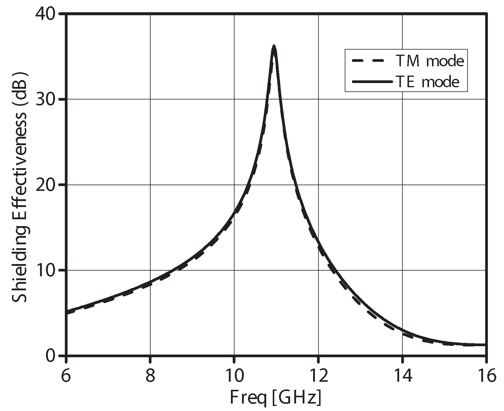
The shielding performance of the proposed FSS under a normal angle of incidence for TE and TM polarizations is presented in
Figure 5. Overall, identical and stable shielding responses at the X-band were observed for both the TE and TM polarizations because of the symmetrical structure of the FSS.
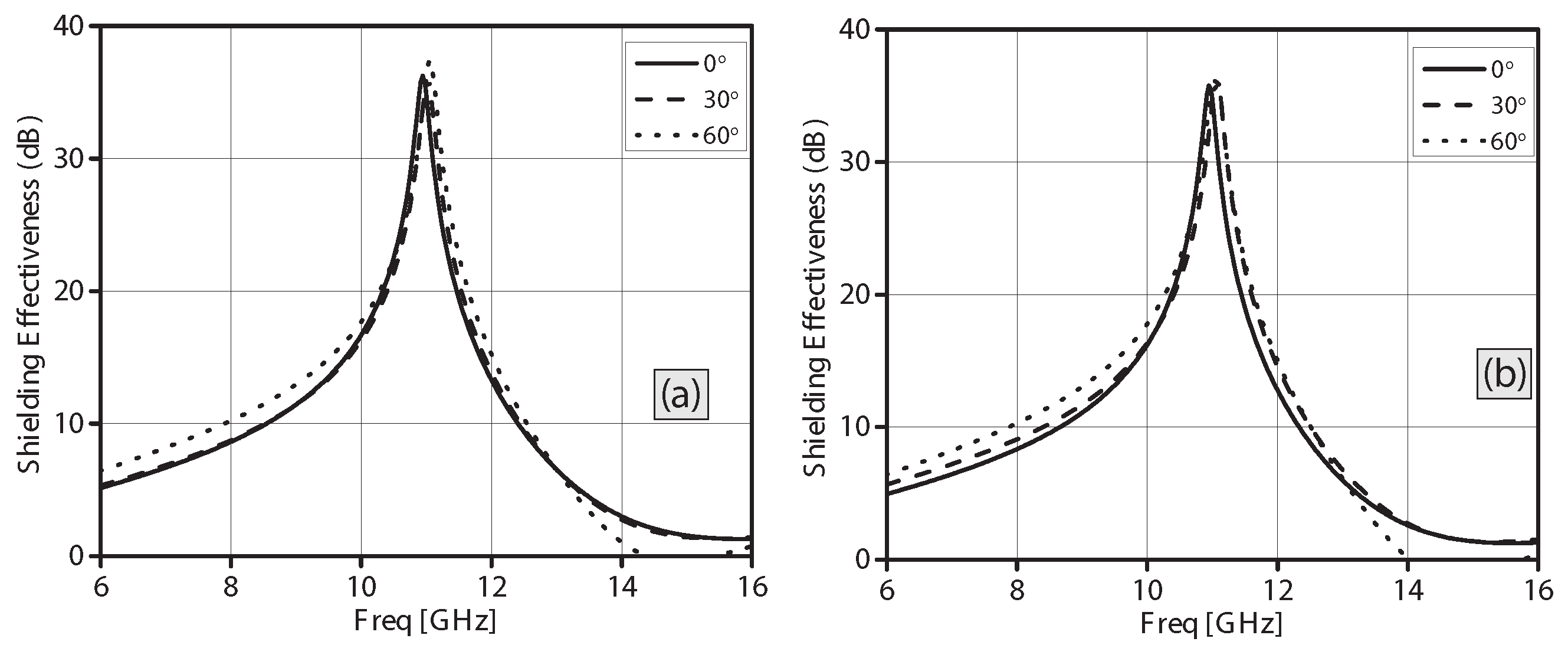
Moreover, the performance of the FSS at various angles of incidence for both the TE and TM polarizations was also analyzed to demonstrate the practicability of the FSS. For performance analysis at various angles, two Floquet ports with TE and TM modes at oblique angles (0°, 30°, and 60°) were used in the simulation model of the FSS. The results showed that the proposed FSS had a stable frequency response for TM polarization at angles varying from 0° to 60°, which correspond to higher modes. In the conventional square-loop FSS unit cell, the absence of the conductive patterns in the inner area resulted in poor angular stability. However, in the proposed FSS unit cell, four inner conductive arms with curved strips covered the inner area and provided greater angular stability for the EM waves arriving from the different angles. Thus, the extended inner arms of the proposed square-loop FSS not only tuned the shielding frequency (
), but also provided stability to the FSS at various angles of incidence. From
Figure 6a, it can be seen that the SE increased from 35 to 39 dB as the angle of incidence was increased from 0° to 60° for TM polarization, with less than 1% change in
. However, for the TE polarization, slight shifts of 1.2% and 1% in
were observed as the angle of incidence was increased from 0° to 60°, respectively. In addition, for the TE polarization,
showed a stable response, as depicted in
Figure 6b.
In addition, a stable frequency response of the proposed FSS at oblique angles and changes in bandwidth at oblique angles for the TM and TE polarizations were observed because of the variation in the surface impedance at oblique angles. A 15 dB bandwidth comparison of both polarizations is shown in
Table 1. It was found that bandwidth increases with an increase in the angle of incidence.
5. Proposed Active FSS
The proposed FSS unit cell shown in
Figure 1 can be reconfigured using PIN diodes (SMP-1322-079LF [
33])to suppress the C-band (6.6 GHz) instead of the X-band. Reconfigurability was achieved by incorporating PIN diodes in the gaps between the adjacent unit cells of the FSS. To demonstrate this reconfigurability, a finite 3 × 3 element FSS was simulated, as shown in
Figure 7a. The PIN diodes were modeled as equivalent RLC boundaries between adjacent cells. The “OFF” and “ON” states of the PIN diodes in the ECM are also shown in
Figure 7a. The PIN diodes act as an open circuit in the “OFF” state. However, for the “ON” state, an additional inductance appears between the unit cells, resulting in the reduction of the shielding resonant frequency to the C-band. The value of
(
Figure 2a) also changes, since there is a capacitance between the adjacent elements, but due to the imperfect nature of metallic strips, a low value of capacitance
still exists, which results in the reduction of the resonant frequency. The response of the reconfigurable FSS is shown in
Figure 7b. It can be confirmed from the figure that the FSS operates in either the X-band or C-band with the PIN diodes in the “OFF” state or “ON” state, respectively. The shielding resonant frequency for the C-band is centered at 6.6 GHz with a 15 dB bandwidth of 2.75 GHz.
Furthermore, to elaborate on the reconfigurability operation of the proposed FSS, induced surface current distributions for a 3 × 3 element shield are plotted in
Figure 8 for both bands. The colors of the arrows show the intensity of the surface currents, while current flow is represented by the direction of arrows. It can be observed in
Figure 8a that the “OFF” state of PIN diodes isolated the flow of current between adjacent elements and resulted in shielding of the X-band. However, for the “ON” state of diodes, the current flowed through them and increased the effective length, resulting in suppression of the C-band. For the TE mode, which is shown in
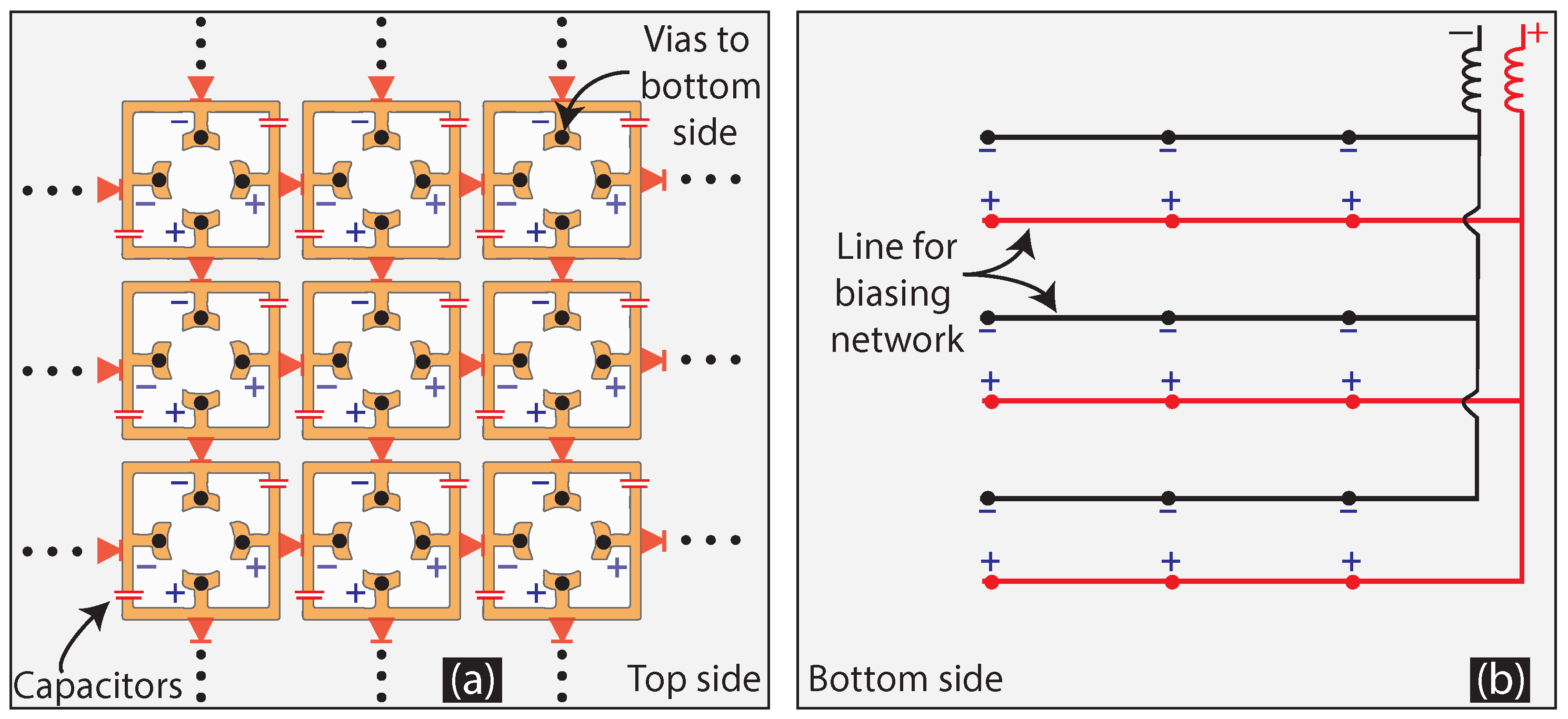
Figure 8b, the PIN diodes in the “ON” state carried a strong current on the left and right sides, whereas a low current intensity can be observed on the top and bottom diodes of the unit element. The PIN diodes were modeled as equivalent lumped elements and simulated using RLC boundary conditions. However, in practical realization, a biasing circuitry is necessary in order to operate these PIN diodes. In this regard, a biasing mechanism was proposed to operate these diodes under forward or reverse bias conditions. The biasing network was designed on the back side of the shield with thin conductive lines, as shown in
Figure 9. These conductive lines were connected to the diodes on the top layer with conductive vias; two diodes were connected to one conductive line, and and the other two were connected to the other conductive line in each unit element. These pairs were isolated using capacitors to avoid short circuiting. Since the biasing circuit was on the bottom side of the FSS, the effect of the DC current on the RF current, which was on top layer, would be at its minimum, and the shielding effectiveness of the FSS would remain the same as that in the simulation results. In addition, the capacitors incorporated on each arm of the FSS in the top layer in the proposed biasing circuitry would avoid short circuiting because of any DC current leakage and would pass the RF current. However, a negligible effect on shielding effectiveness may exist because of the stray capacitance. Therefore, it can be argued that the incorporated capacitors will have a negligible effect on the overall shielding effectiveness of the proposed FSS.
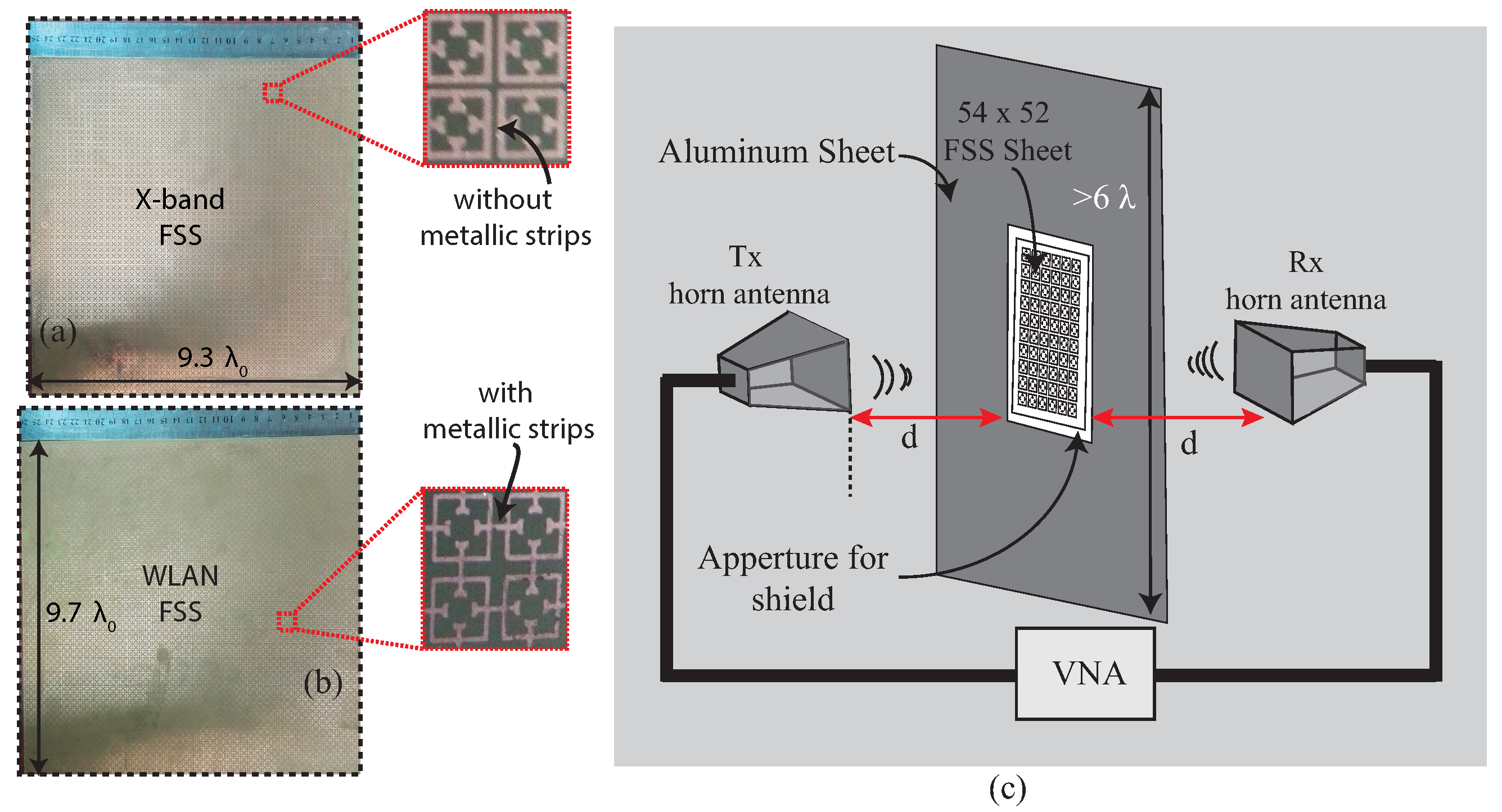
6. Measured Results
To validate the proposed designs, two separate shields were fabricated. One shield had no connections between unit elements, representing the “OFF” state of the PIN diodes, and the other one had shorting strips, representing the “ON” state. Both shields were fabricated on an FR4 substrate with
= 4.4, tan
= 0.02, and 1.6 mm thickness. Each shield had 54 × 52 elements. Pictures of the FSS prototypes fabricated with and without metallic strips to mimic PIN diodes’ “ON” and “OFF” states, respectively, are shown in
Figure 10a,b. The overall size of the fabricated prototype was 9.78
× 9.32
at a frequency of 11 GHz. To measure the shielding effectiveness of the fabricated prototype, a rectangular aperture with dimensions 240 mm × 240 mm was created in an aluminum sheet with size 260 mm × 250 mm (greater than 6
). This was done to ensure that the EM plane wave was only transmitted through the FSS fixed in the aperture. Two identical broadband horn antennas (model#LB-20265) [
34] were used as a transmitter and receiver. A block diagram of the experimental setup used for the measurements is shown in
Figure 10c. Furthermore, to ensure the efficacy and accuracy, a two-stage measurement process was adopted where, in the first stage, the reference measurement of
was carried out through the aperture without a shield. This reference measurement was performed to measure the free-space transmission through the aperture. Then, In the second stage, the shields were placed in the aperture and measured with reference to the calibration. Similarly, for angular stability measurements, the setup was rotated at different angles.


 ,
, 


