Article

Synchronous Control Strategy with Input Voltage Feedforward for a Four-Switch Buck-Boost Converter Used in a Variable-Speed PMSG Energy Storage System

1
College of Information and Control Engineering, Weifang University, Weifang 261061, China
2
School of Electrical Engineering, Southeast University, Nanjing 210096, China
*
Author to whom correspondence should be addressed.
Electronics 2021, 10(19), 2375; https://doi.org/10.3390/electronics10192375
Submission received: 3 September 2021 / Revised: 24 September 2021 / Accepted: 27 September 2021 / Published: 28 September 2021

Abstract

:
The four-switch Buck-Boost (FSBB) converter can produce voltage conversion within a wide input voltage range, which is suitable for variable-speed permanent magnet synchronous generator (PMSG) energy storage systems with AC inputs and DC outputs. To reduce the interference of input voltage fluctuation on the performance of the FSBB converter, an input voltage feedforward (IVFF) compensation method is proposed in this paper. The switching synchronization strategy is simple. Using the switching average model, the small signal model of a non-ideal FSBB converter in all working modes is established. The effects of input voltage, load current, damping coefficient and right half plane (RHP) zero on the stability of the control system are analyzed in detail. The transfer function of the IVFF of the FSBB converter is derived, and the relationship between input voltage, load current and duty cycle is analyzed. Finally, the design of the parameters of the converter control system is presented. The simulation and experimental results show that this FSBB converter has high efficiency and a good transient response.

Graphical Abstract

1. Introduction

As independent power supplies, generator energy storage systems are widely used in automobile, communication and other engineering fields. Compared with traditional-mechanism generator systems, PMSG energy storage systems offer the advantages of small volume and convenient carrying [1,2,3,4,5].
A variable-speed PMSG power supply system, which features a DC-DC converter to regulate DC voltage, is shown in Figure 1. The PMSG works at a variable speed and it is driven by a drag device. The amplitude and frequency range of the AC voltage are changed. The AC voltage output by the PMSG is converted into a pulsating DC voltage by a rectifier circuit, and then the pulsating voltage is converted into a constant voltage by a DC-DC converter [6,7,8]. Therefore, DC power supply or energy storage systems, especially those with AC input and DC output, need step-up/step-down converters, particularly aerospace equipment power supply and automotive power supply systems.
In DC-DC converters, Buck or Boost converters have a single conversion function and cannot be directly applied to circuits with wide voltage ranges. DC-DC converters with step-up/step-down voltages include single-switch Buck-Boost, Cuk and Sepic/Zeta. The single-switch Buck-Boost output voltage has an opposite polarity. Although it can be used in high-power circuits, it poses the problems of high switching stress and complex control [9,10]. Cuk and sepic/zeta converters include many passive components, experience high power loss in capacitance and inductance energy conversion, offer a relatively low power density, and cannot be used in high-power circuits [11,12,13].
The FSBB converter is composed of a synchronous Buck converter and a Boost converter in cascade. The polarity of the output voltage of the FSBB is the same as that of the input voltage. The circuit topology is simple, easy to miniaturize, and can be used in high-power automotive energy storage circuits [14,15,16]. Currently, FSBB is reported to be used in a power supply system composed of lithium batteries [17,18], and to improve the power factor of power grids [19].
In the above research, the input DC voltage fluctuation of the FSBB converter is small, as is the ripple amplitude of the low-frequency AC voltage. In the variable-speed PMSG energy storage system, the AC voltage range of the generator output is wide, and the output voltage of the uncontrolled rectifier fluctuates greatly. The wide-range fluctuation of the input voltage changes the operating point of the FSBB converter control system, and even leads to its instability. At present, there are few research results of DC-DC converters applied to variable speed generators. Therefore, it is necessary to study a DC-DC converter suitable for a PMSG energy storage system.
A wide-input voltage range FSBB converter control method suitable for variable-speed PMSG is proposed. To reduce the influence of variable-speed PMSG output voltage disturbance on the FSBB converter, an IVFF method with synchronous operating modes is proposed. Considering the working voltage and current of the FSBB converter, a small signal model of an FSBB converter is presented. The influence of the circuit parameters on the control system is analyzed. Finally, the analysis, design and performance are verified by a prototype.

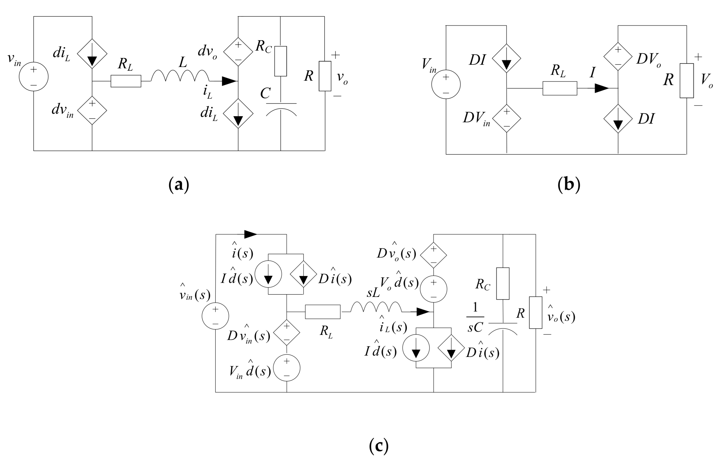
2. Circuit Structure and Analysis of FSBB Converter

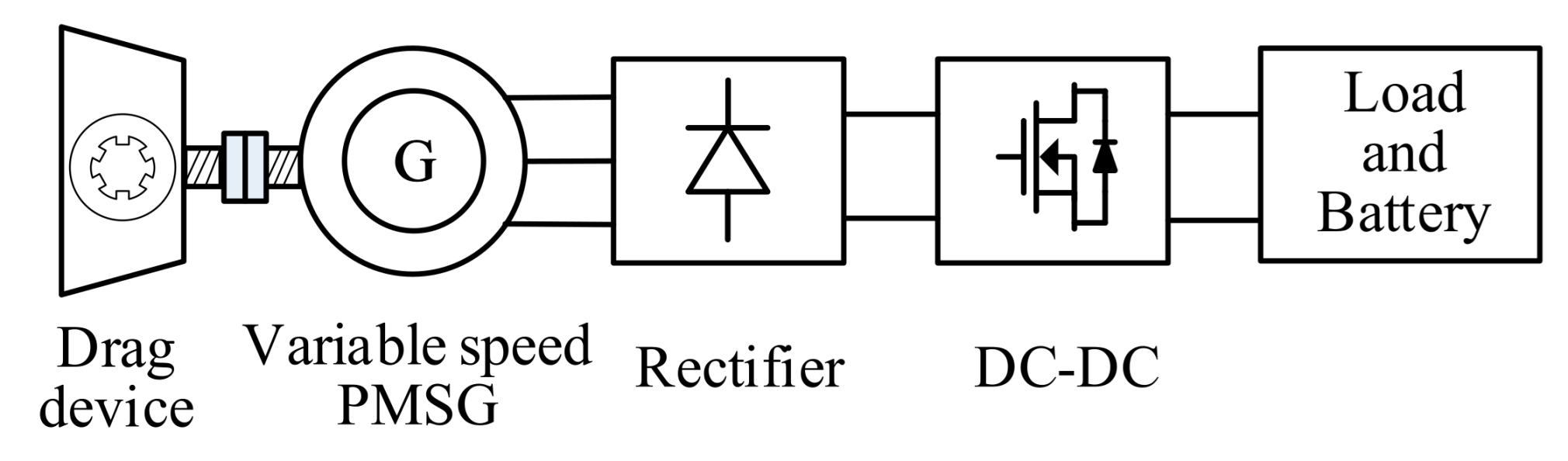
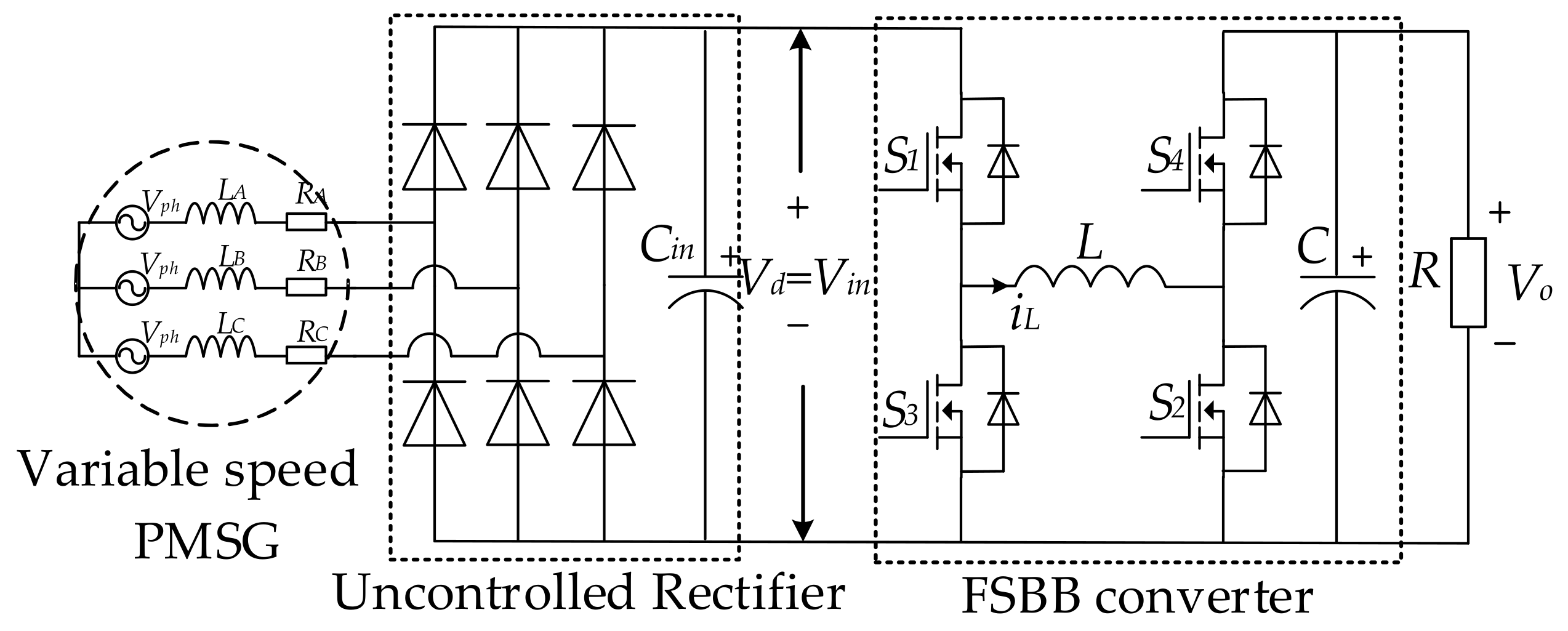
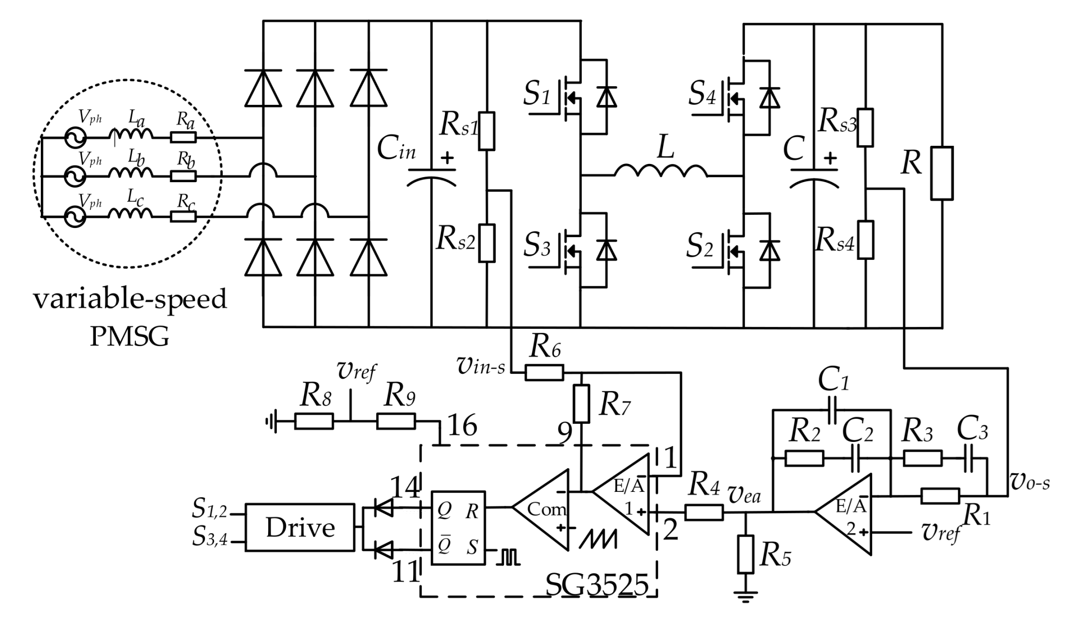
2.1. Circuit Structure of Storage System

Variable-speed PMSG energy storage systems include a variable speed PMSG, rectifier circuit and FSBB converter, as shown in Figure 2. The FSBB consists of four switches (S1, S2, S3, S4), an L filter inductor, and a C filter capacitor. Cin is the rectifier output filter capacitor. R is the load resistance. Vph is the root mean square value of the three-phase phase voltage. Vd is the rectified voltage.
The output voltage of the variable-speed PMSG fluctuates greatly, and the FSBB converter adopts a synchronous switch control mode. The S1 and S2, S3 and S4 of the FSBB all work in high-frequency synchronization mode. The control circuit uses a compensation circuit and a pulse width modulation circuit. The converter control system features a simple design and high reliability. The waveforms of the synchronization control mode are shown in Figure 3. VS1,2 and VS3,4 are the switching signals. Vin is the input DC voltage. VL is the inductor voltage. The iL symbol represents the instantaneous value waveform of the inductor current. Vo means the output DC voltage. T is the switching cycle period. D is the duty cycle.
When the FSBB converter operates in a steady state, Vin is equal to Vd. When S1, S2 are turned on, the VL is equal to Vin; when S3, S4 are turned on, the VL is equal to −Vo. The minus of −Vo indicates that the polarity of VL is reversed. In Figure 3, the value of VL is equal to Vo in the negative Y axis for VL. In one switching cycle, according to the volt-second balance principle, the relationship between the Vin and Vo of the FSBB is
V o V i n = D 1 D
The expression of the average value of the converter output current Io and the average value of inductor current IL is
I o = ( 1 D ) I L
The control system of the DC-DC converter is a typical negative feedback system. In this study, the converter’s actual output voltage was compared with a given voltage, the stability of converter was analyzed, and the adjustment parameters of control system were designed. Finally, the PWM signal was obtained. It was necessary to analyze the small-signal model of the FSBB converter before designing the control circuit.
The DC-DC converter operates in the switching state, and the control system features strong nonlinear characteristics, so it is difficult to accurately analyze the dynamic characteristics of the system. The small-signal modeling method commonly used in DC-DC converters is the state space average method [20]. The average circuit model of the FSBB converter is established, which is essentially the equivalent controlled source circuit model of the converter. A small-signal control model of FSBB can be derived according to the circuit theorem, and this derivation process is simple. In this model, the fully controlled switch and diode are equivalent to the corresponding controlled source. Figure 4 is the switching average circuit of the non-ideal FSBB converter.
Figure 4a is the equivalent controlled source circuit of the FSBB converter, where switches S1 and S2 are equivalent to controlled current sources, and S3 and S4 are equivalent to controlled voltage sources. Figure 4b is the DC equivalent circuit. L is short-circuited, RL is the equivalent series resistance of L. C is open-circuit. Figure 4c is the AC small-signal equivalent circuit. RC is the capacitor equivalent series resistance. In Figure 4, capital letters indicate the DC steady state value of the converter, and lowercase letters with a hat (^) indicate the AC small signal disturbance value.

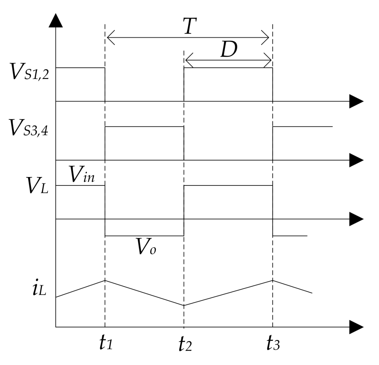
2.2. Main Transfer Function

The key transfer function of FSBB converter is derived according to Kirchhoff’s law of voltage and current. The transfer function of the FSBB converter control signal d(s) to the output voltage vo(s) is
G v d ( s ) = v o ( s ) d ( s ) = G v d o ( 1 + s ω Z C ) ( 1 s ω R H P Z ) 1 + 2 ξ s ω o + ( s ω o ) 2
where,
G v d o = R ( 1 D ) ( V i n + V o ) R L V o / ( 1 D ) R L + R ( 1 D ) 2 , ω o = R L + R ( 1 D ) 2 ( R C + R ) L C , ω z c = 1 R C C ,
ξ = R L R C + R C R C ( 1 D ) 2 + R L R C C + L 2 [ R L + R ( 1 D ) 2 ] ( R C + R ) L C , ω R H P Z = R ( 1 D ) 2 R L L + R ( 1 D ) 2 L V i n V o .
In the continuous operating mode of the inductor current, the transfer function Gvd(s) of the converter features RHP zero. Table 1 shows the circuit design parameters of the AC-DC converter. Vd is Vph multiplied by about 2.34~2.45. Vd = 2.45Vph was chosen in this study.

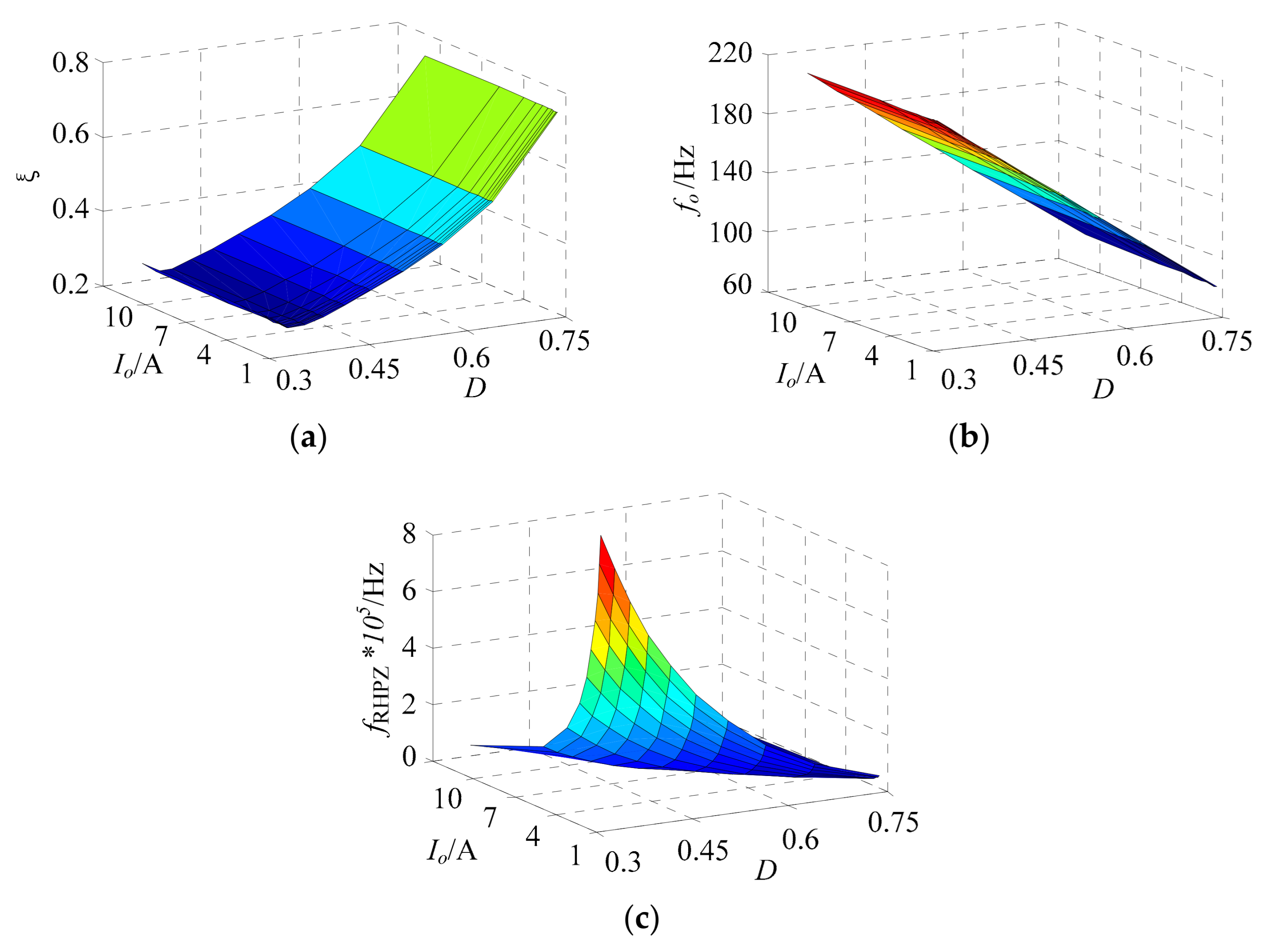
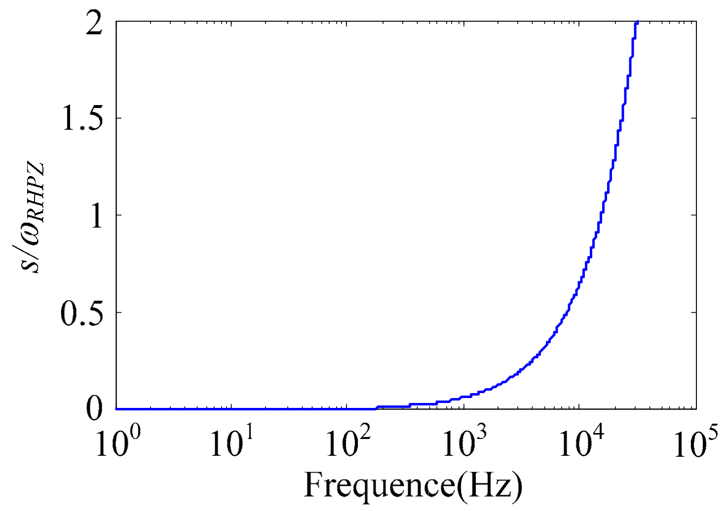
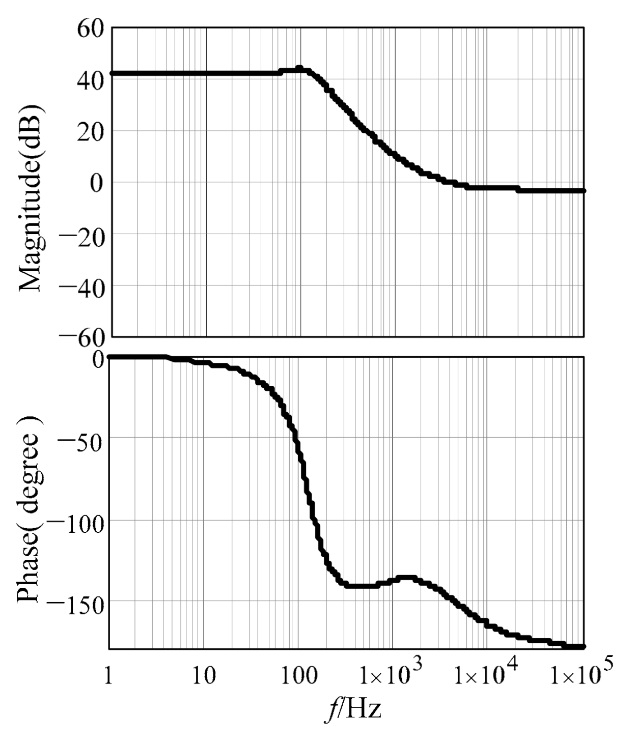
2.3. Right-Half-Plane (RHP) Zero

According to the circuit design parameters, in the wide line voltage range from 17 V to 50 V for a load of 300 W, the duty cycle D is 0.29 to 0.54. D follows the change of input voltage, and D affects the resonant frequency f0 = ωo/2π and the RHP zero frequency fRHPZ = ωRHPZ/2π of the system. In Figure 5a, as the input voltage of the FSBB converter increases, D and ξ reduce. Under the same D, when Io changes, ξ remains unchanged. As seen from Figure 5b, D decreases and the resonant frequency f0 decreases. The f0 is less than the low-frequency ripple frequency of the output voltage; f0 does not affect the stability of the system. As shown in Figure 5c, the value of fRHPZ increases as in line with the input voltage. When the AC voltage is 17 V, fRHPZ is about 4 kHz. Under the synchronous control mode, fRHPZ has little relationship with the phase margin of the converter.
When the input voltage of maximum power for 300 W changes, the open loop control system’s pole-zero distribution and the step response of the system in accordance with the different duty cycles, as shown in Figure 6.
As shown in Figure 6a, as Vin increases, D is reduced from 0.54 to 0.29. The left-half-plane poles and the RHP zero trajectory of the system in the S plane move away from the origin, which reduces the damping of the control system, and the overshoot of the step response becomes large. Corresponding to the analysis in Figure 6b, with the increase of D, the step response overshoot increases, and the transition time becomes longer. The RHP zero point of the control system is far away from the origin, and the negative overshoot of the system response is reduced. The foregoing analysis shows that negative overshoot decreases as D decreases, the change of the D value has an obvious influence on the transient characteristics of the FSBB converter. This characteristic is consistent with the overshoot response caused by the decrease of ξ as a consequence of the decrease of D, as shown in Figure 5a.
In Figure 7, the input voltage remains constant and the load Io changes from 1A to 10A. The open loop control system’s pole-zero distribution and the step response of the system at different load Io were studied. As shown in Figure 7a, the RHP zero point trajectory of the system in the S plane is close to the origin of the Io increase, and the trajectory of the left-half-plane pole on the imaginary axis does not change. In Figure 7b, the overshoot changes less with the increase of Io. When the RHP zero point moves to the origin, the negative overshoot of the controller increases. According to the above analysis, the negative overshoot increases with the increase of Io. The change of Io has little effect on the dynamic performance, which is the same as the characteristic of the damping ξ changing with the load Io, as shown in Figure 5b.

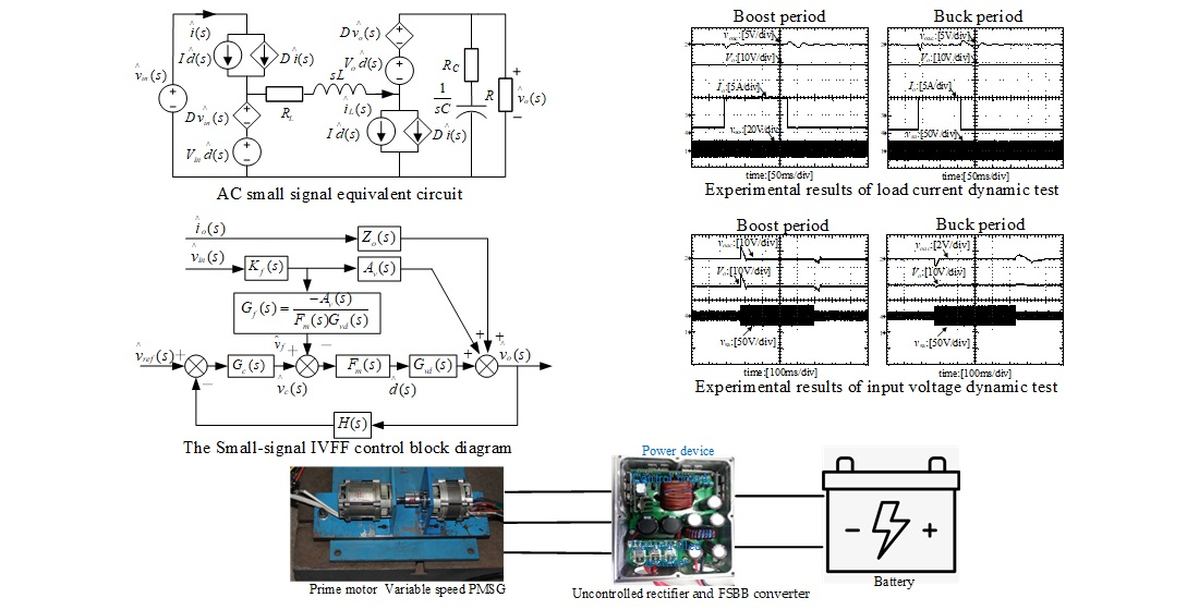
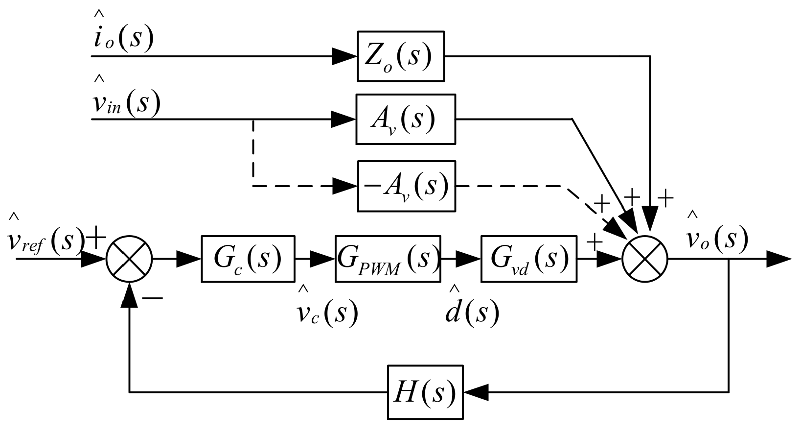
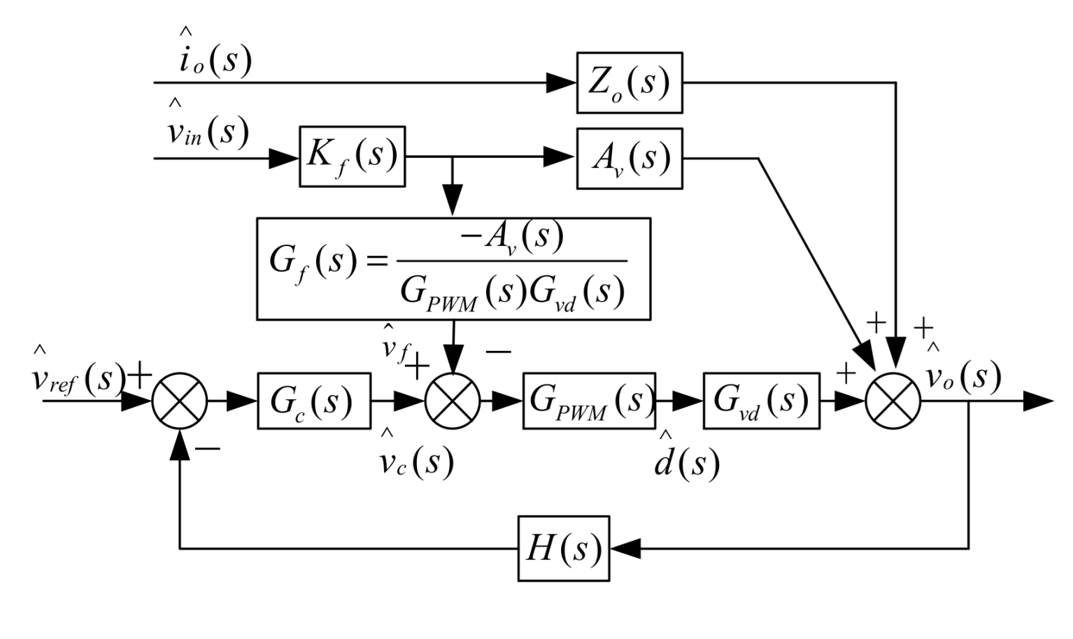
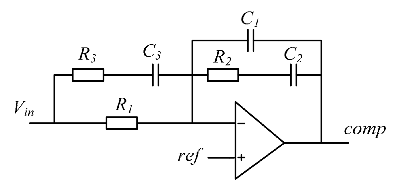
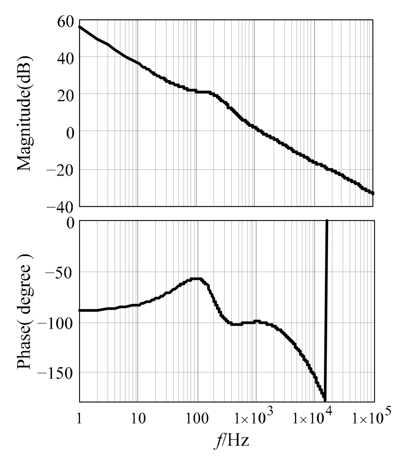
3. IVFF Control System Analysis

Figure 8 shows the small-signal control block diagram [21,22]. Gvd(s) is the transfer functions of the D to Vo. Av(s) is the transfer functions of Vin to Vo. Zo(s) is the transfer functions of Io to Vo. Gc(s) is the transfer function of the voltage regulator. H(s) is the sense gain of Vo. GPWM(s) is the PWM modulation.
The disturbance component v ^ i n of the converter Vin affects Vo through the path of Av(s). In order to reduce the impact, a transfer function −Av(s) was added to schematic diagram, as shown by the dotted line in Figure 8. Figure 9 is the small-signal IVFF control block diagram. The output terminal of −Av(s) is transferred to the output side of Gc(s). The modified module is named Gf(s). Kf(s) is the sense gain of Vin.
The IVFF path is from v ^ i n to v ^ f The transfer function Gf(s) is derived as
G f ( s ) = v ^ f v ^ i n = A v ( s ) G P W M ( s ) G v d ( s ) = R D ( 1 D ) 2 R ( 1 D ) 2 ( V i n + V o ) R L V o V m ( 1 s ω R H P Z ) = D ( 1 D ) 2 ( 1 D ) 2 ( V i n + V o ) R L I o V m ( 1 s ω R H P Z )
where, Vm is peak to peak value of carrier wave, and ωRHPZ is the RHP zero. In this paper, Vm = 2.4 V. In Formula (4), due to the existence of the RHP zero of transfer function, the bandwidth and transient response of the control system are limited. A two-zero three-pole compensation network Gc(s) is designed to improve the control performance of the FSBB converter.
As discussed earlier, the transfer functions of Vin to Vo can be derived as
A v ( s ) = v o ( s ) v i n ( s ) = A o 1 + s ω Z C 1 + 2 ξ s ω o + ( s ω o ) 2
where, A o = R D ( 1 D ) R L + R ( 1 D ) 2 .
The transfer function GPWM(s) can be expressed as
G P W M ( s ) = 1 V m
In Formula (5), the term s/ωRHPZ is a function of frequency. When the converter is fully loaded and the input voltage is at its maximum, the s/ωRHPZ factor reaches its maximum value. According to the parameters of the FSBB converter in Table 1, when the FSBB converter is fully loaded (R = 2.7 Ω) along with the maximum input DC voltage (Vin = 70 V), the amplitude-frequency curve of s/ωRHPZ is as described in Figure 10.
As can be seen from Formula (6), the DC component Gf of the transfer function Gf(s) is related to the Vin and Io. Under different load conditions of the converter, the variation curve between Gf and the input voltage is as shown in Figure 11. Gf is very sensitive to load current. In this study, a compromise scheme was selected, and Io was set to 55 % Io-dc.
According to Figure 9, the loop gain is
T ( s ) = H v ( s ) G c ( s ) F m ( s ) G v d ( s )
Assuming that Gc(s) = 1, the loop gain before compensation can be obtained by substituting Gvd(s) into Formula (7). The Bode diagram of T(s) before correction is shown in Figure 12. The low frequency gain is 41dB. The phase margin at the cut-off frequency of transfer function is 30 degrees. In addition to RHP zero, the converter has LC double poles, and a capacitor ESR zero. To improve the control performance of the FSBB, the two-zero, three-pole compensation network was selected, as shown in Figure 13.
The transfer function of the compensator network is
G c ( s ) = K ( 1 + s ω c z 1 ) ( 1 + s ω c z 2 ) ( 1 + s ω c P 1 ) ( 1 + s ω c P 2 )
where K = 1 R 1 ( C 1 + C 2 ) , ω c z 1 = 1 R 2 C 2 , ω c z 2 = 1 ( R 1 + R 3 ) C 3 , ω c p 1 = 1 R 3 C 3 , ω c p 2 = C 1 + C 2 R 2 C 1 C 2 .
In the voltage control method, the cut-off frequency of control system is generally 1/8~1/5 times the switching frequency [10]. The transfer function of the FSBB converter has RHP zero point, and the frequency is more than 4 kHz. The cut-off frequency is set to 1 kHz to reduce the influence of RHP zero on control performance. The two zeros of the compensator are used to compensate the double poles of LC, and the two poles are used to compensate the ESR zero and the RHP zero. The resistance value and capacitance value are as follows, respectively: R1 = 100 kΩ; R2 = 35 kΩ; R3 = 5 kΩ; C1 = 820 pF; C2 = 220 nF; C3 = 10 nF.
Figure 14 is the Bode diagram of T(s) after compensation. After the converter control system is compensated, the DC gain in the low frequency band becomes larger, and the phase margin at the cut-off frequency is increased to 78 degrees.
In Figure 14, the control system has a sufficient phase margin. However, the cut-off frequency is low, the bandwidth is narrow, and the dynamic performance is poor when the wide Vin range changes. Therefore, based on the compensation network Gc(s), the influence of IVFF compensation on the transient Vin of the FSBB converter was further studied. According to Figure 9, the closed-loop transfer function of Vin to Vo with IVFF compensation is
Φ v v ( s ) = v o ( s ) v i n ( s ) = A v ( s ) + G f ( s ) F m ( s ) G v d ( s ) 1 + T ( s )
Substituting Gf(s), Av(s) and Gvd(s) into (9), the magnitude of Φvv under different input voltages with IVFF compensation and without IVFF compensation, as shown in Figure 15a, can be obtained. The results show that the FSBB converter with IVFF compensation can suppress the disturbance of Vin under the condition of wide input. In the low frequency range, the control effect of boost mode is better than that of step-down mode. As shown in Figure 15b, the Io has a small effect on Φvv.

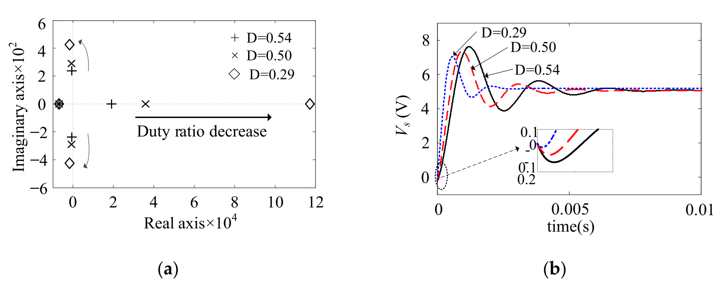
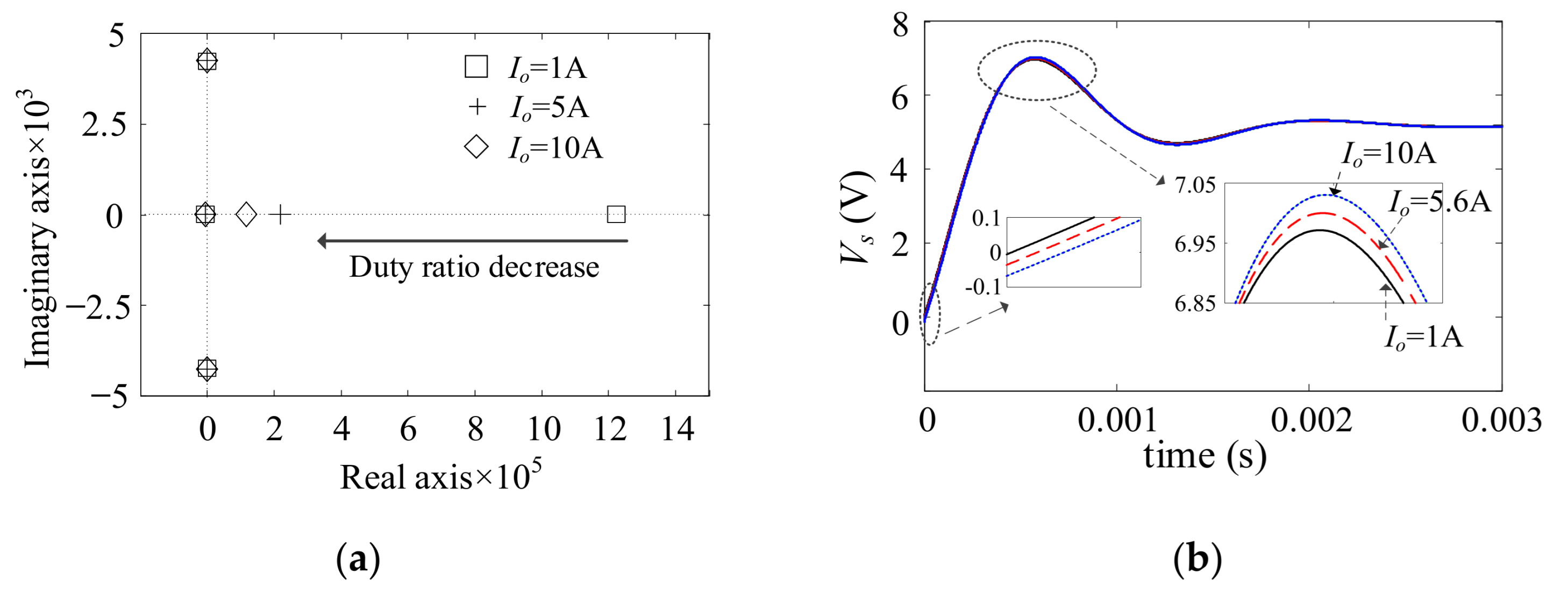
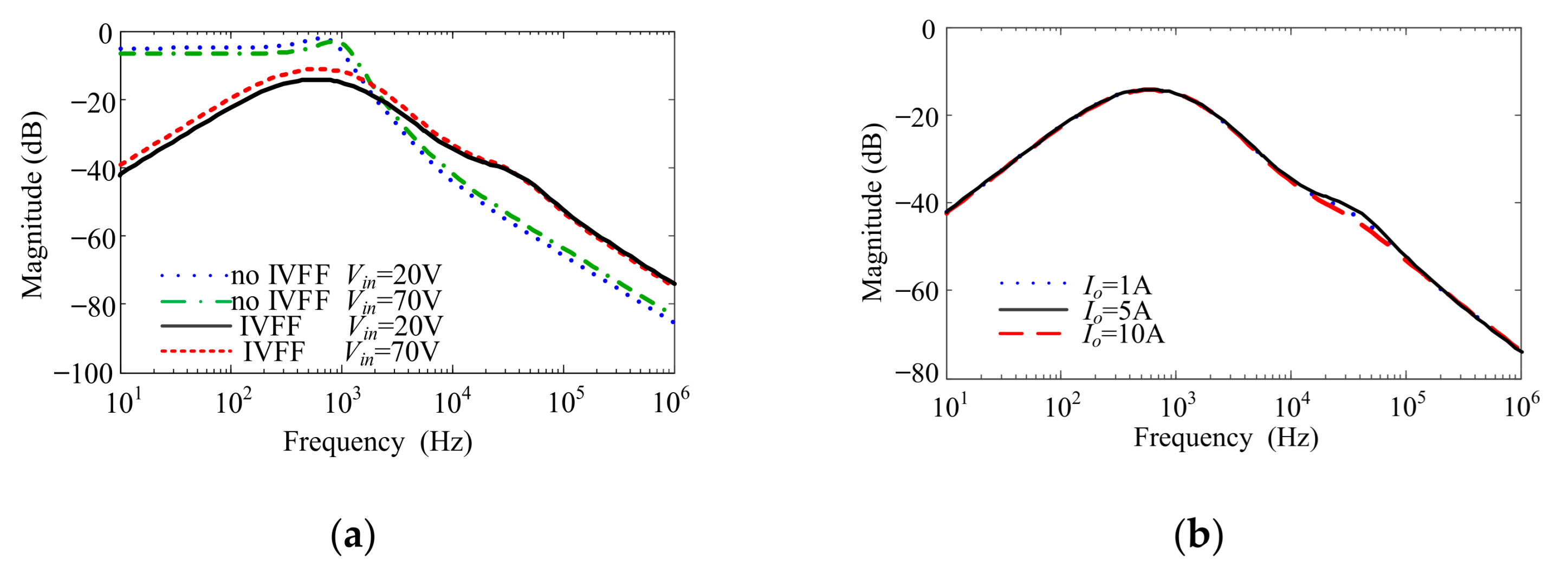
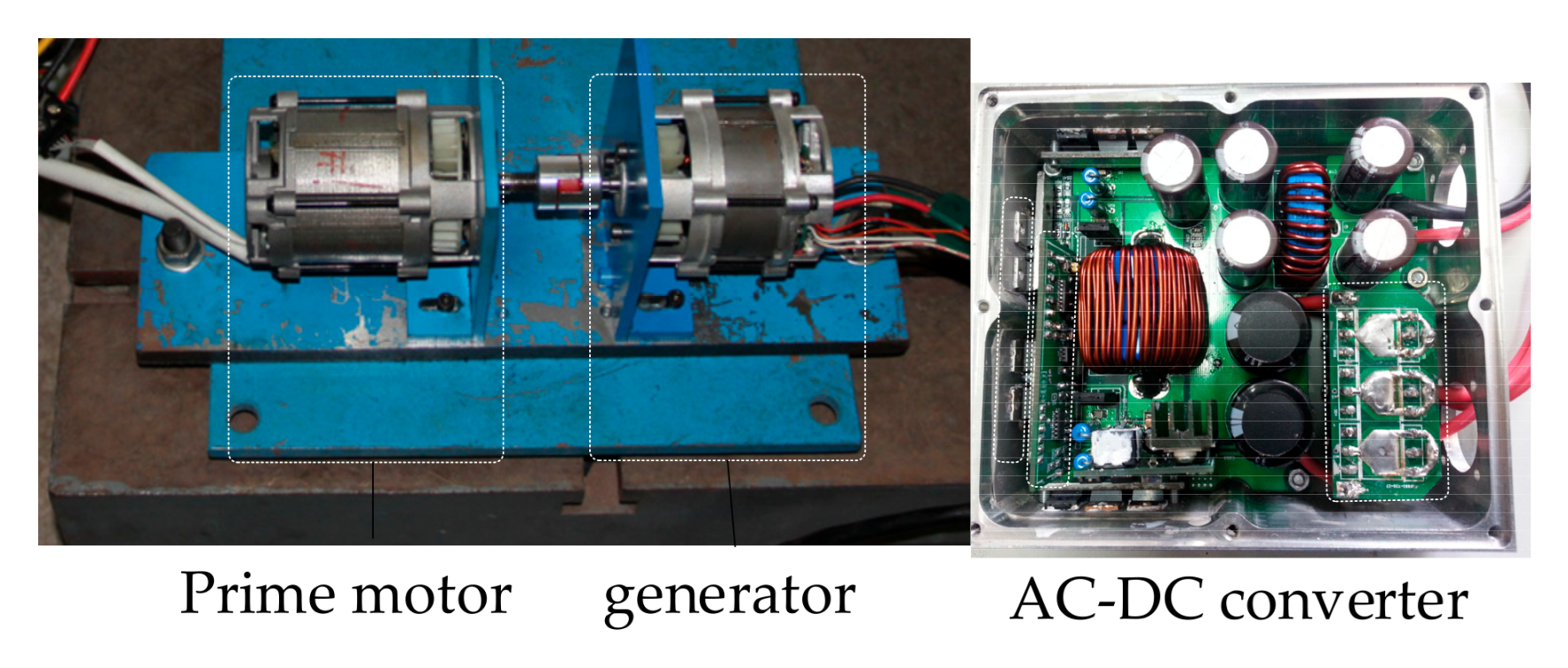
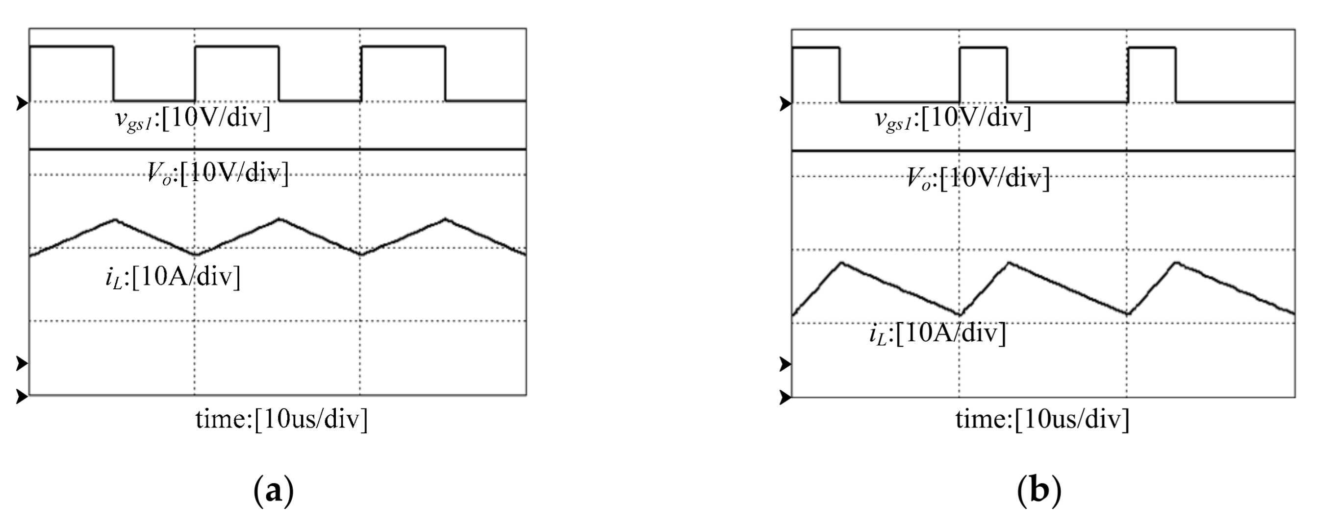
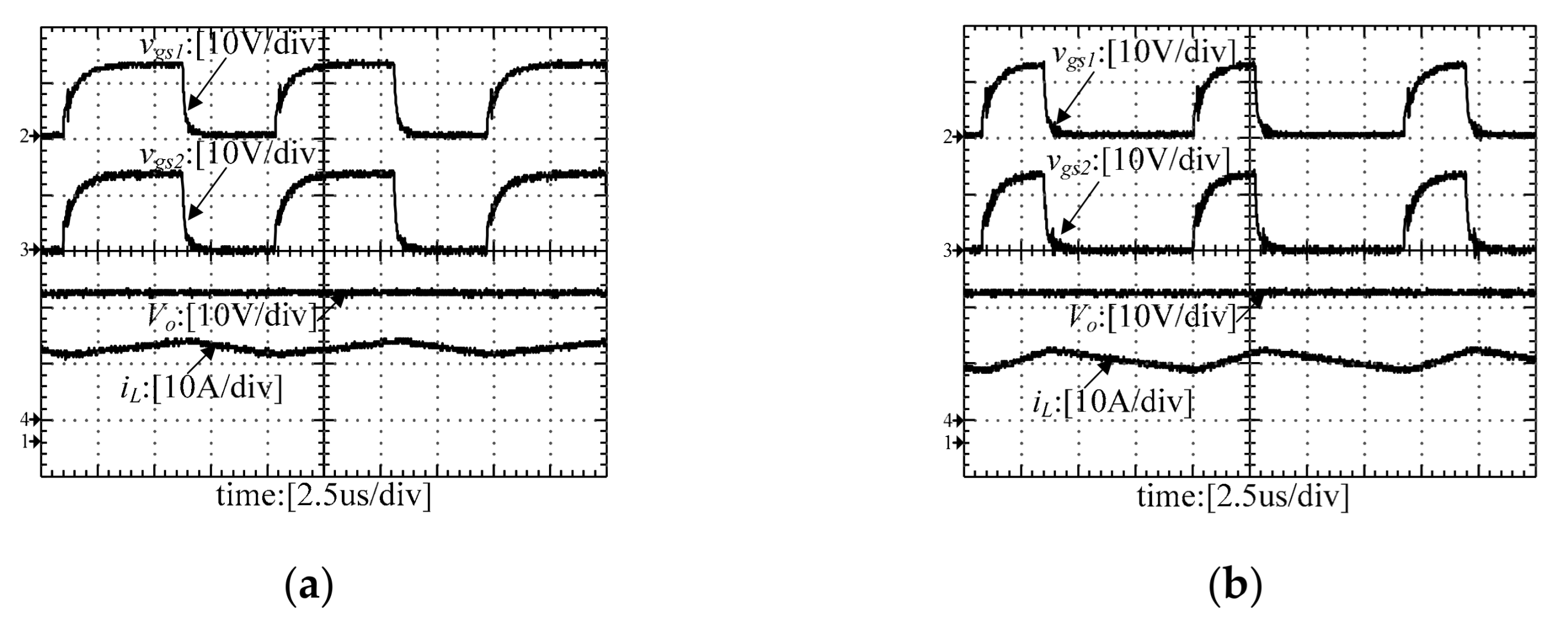
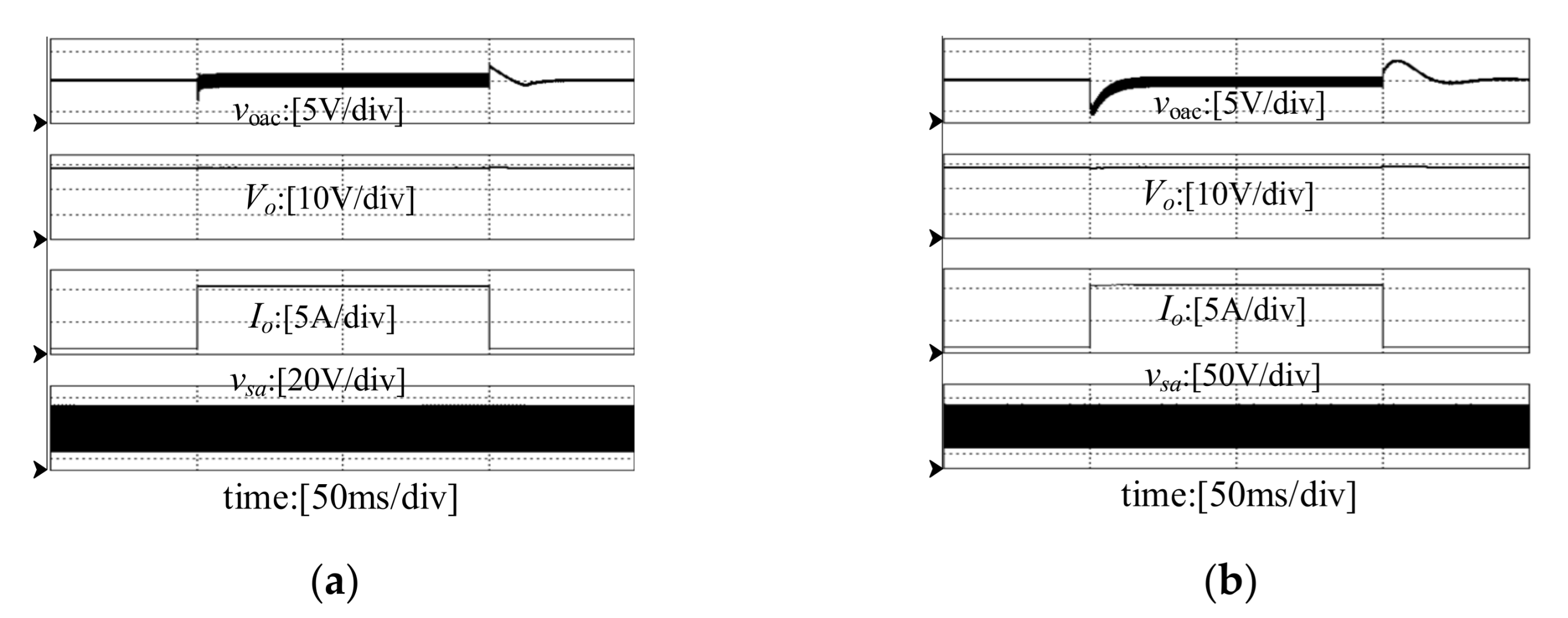
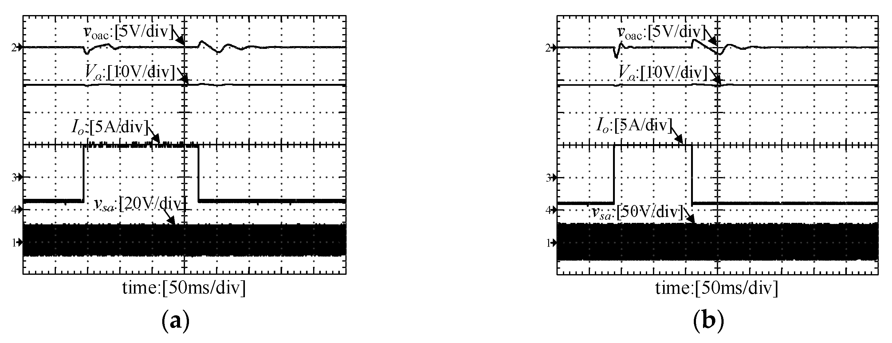
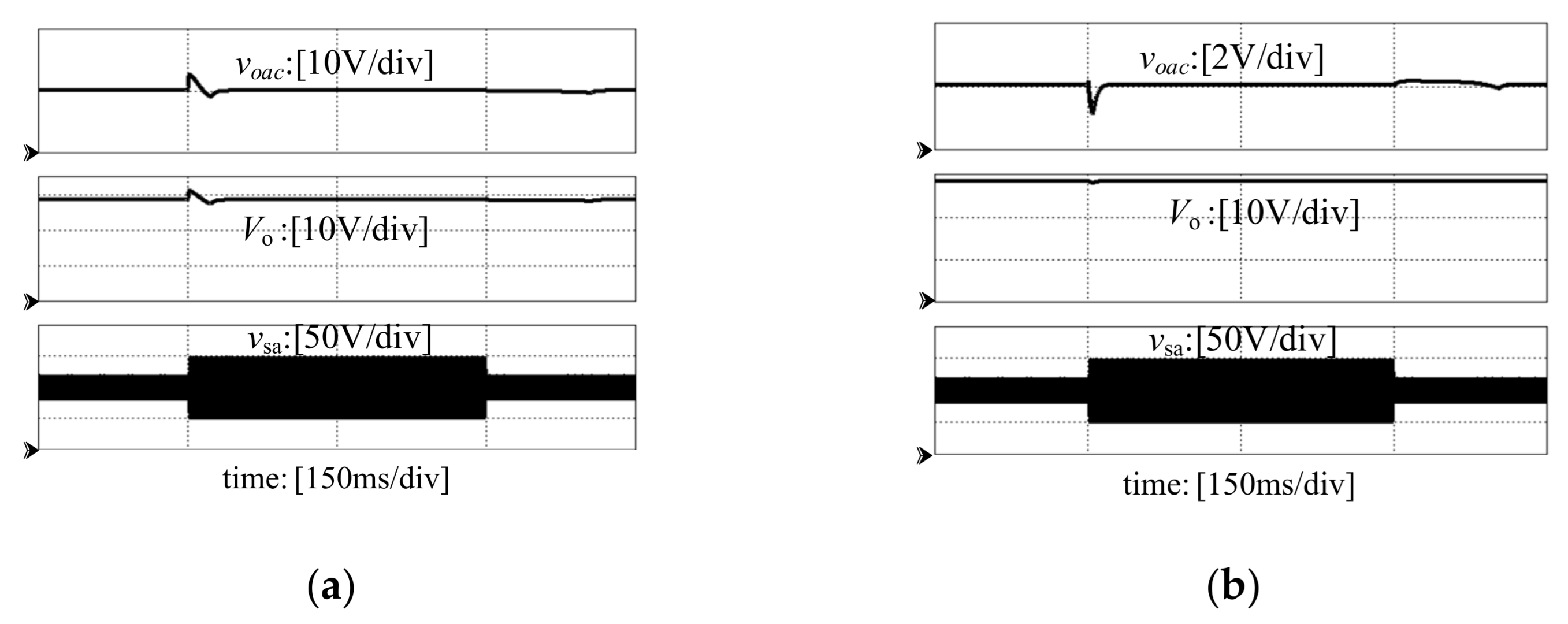
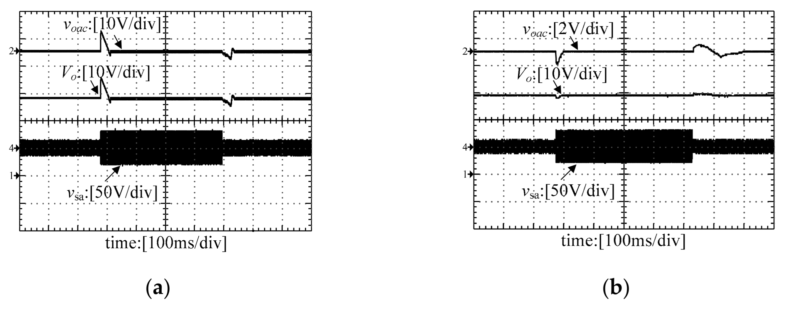
4. Experimental Verification

The diagram under synchronous switching mode with the IVFF method is shown in Figure 16. v i n s = V i n R s 4 / ( R s 3 + R s 4 ) is the input signal of the input voltage feedforward circuit, where Rs3 = 200 kΩ, Rs4 = 10 KΩ. vea is the output of compensator, v o s = V o R s 2 / R s 1 + R s 2 is the output voltage signal detection value, where Rs1 = 47.5 kΩ, Rs2 = 10 kΩ, and vref = 5 V obtained by the resistor divider with R8 = 10 kΩ, R9 = 200 Ω from the vref pin of SG3525. Combining (8) and (10), the values of R4R7 are as in Figure 16. An FSBB converter under a synchronous switching control scheme with IVFF can be obtained when R4 = R6 = 20 kΩ, R5 = R7 = 50 kΩ, respectively, in the practical circuit.
v e = ( R 7 R 6 + 1 ) R 5 R 4 + R 5 v e a R 7 R 6 v i n s
To verify the effectiveness of the above theory and calculation, an experimental platform was built in the laboratory, and a 300 W AC-DC converter was designed, as shown in Figure 17.
The steady-state waveforms are shown in Figure 18 and Figure 19; vgs is the control signal of the switch. Figure 18 shows the simulation results. The Vo of the converter remains stable in both Buck and Boost periods. Figure 19 shows the experimental waveforms, which were consistent with the simulation results.
Figure 20 and Figure 21 show the Io dynamic test waveforms of the AC-DC converter. The load current jumps within the range of 1 A to 10 A. vsa is the three-phase line voltage. Figure 20 shows the simulation results. When the load current is stepped, the output voltage fluctuation value is 1 V, and the AC component voac of Vo is less than 200 mV. Figure 21 shows the experimental results of the Io dynamic test. When the Io changes suddenly, the output voltage of the Buck period fluctuates greatly, the output voltage fluctuation value reaches 1.5 V, and the AC component in the output voltage is about 400 mV. The converter displays good dynamic characteristics of load current.
Figure 22 and Figure 23 are the waveforms of the AC input voltage dynamic test. When the converter runs at a rated load, the three-phase line voltage steps between 17~50 V. It can be seen from the simulated and experimental waveforms that the IVFF compensation method improves the transient response of Vo.
Figure 24 is the efficiency curve. The AC-DC converter has high efficiency in the three-phase line voltage between 5~50 V.

5. Conclusions

In this paper, a synchronous control strategy with IVFF compensation for the FSBB converter is proposed. The converter can convert a voltage of 10 times the width into a constant value, which can be used in vehicle converters. The research conclusions are as follows:
(1)
In synchronous control mode, the FSBB converter has a simple structure and low switching stress. The voltage ratio is high.
(2)
The small-signal model of the FSBB has RHP zero, which is related to the duty cycle and load. The two-zero and three-pole compensation scheme improves the transient response of the FSBB converter within a wide input range.
(3)
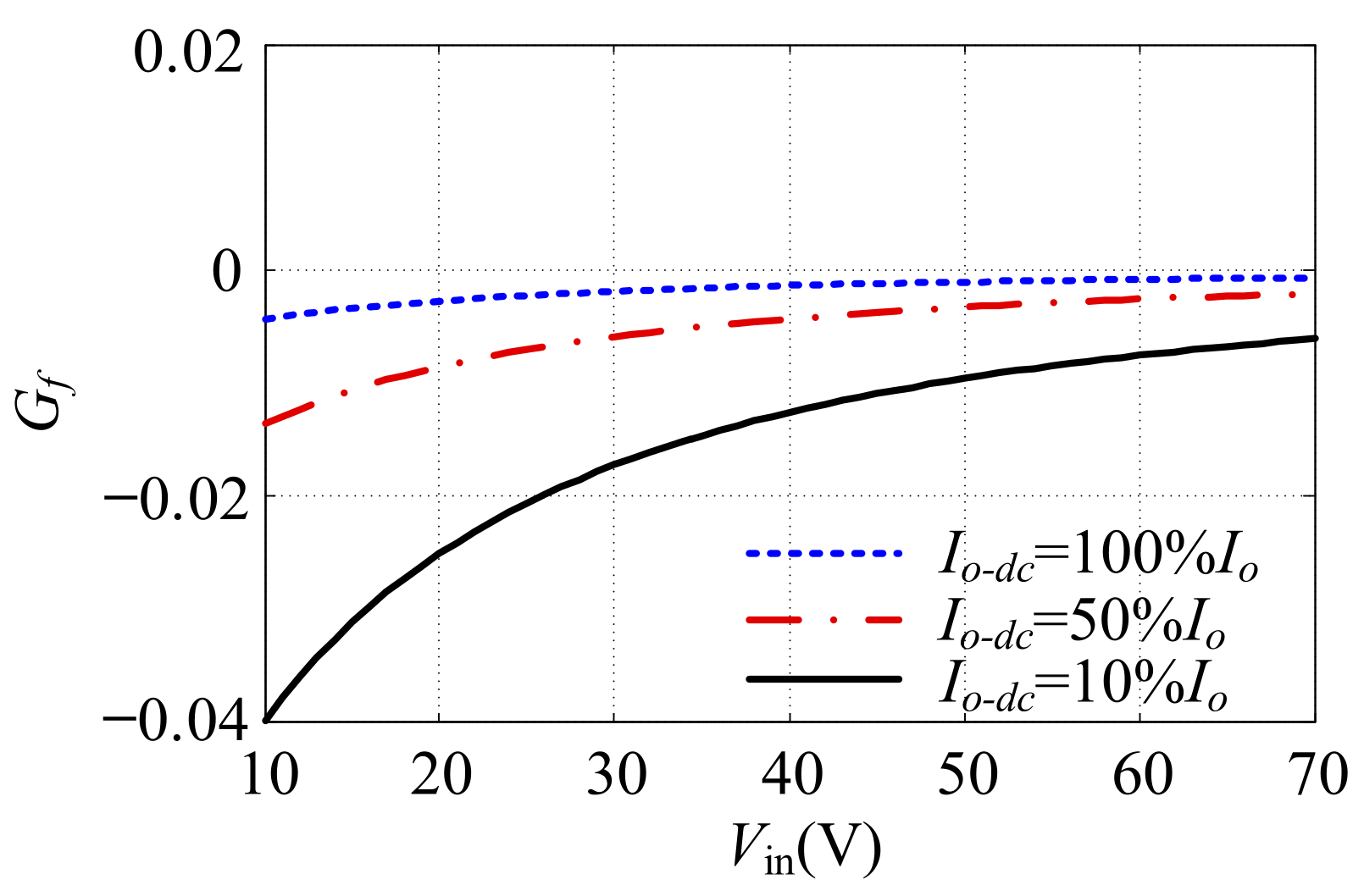
The IVFF compensation method can reduce the interference of input voltage. Due to the influence of the RHP zero, the ability to suppress the input voltage disturbance with input voltage feedforward is weaker in the high-frequency band.

Author Contributions

Conceptualization, L.T. and M.L.; methodology, L.T. and J.W.; software, L.T.; validation, L.T. and J.W.; formal analysis, L.T.; writing—original draft preparation, L.T.; writing—review and editing, M.L. and C.H.; visualization, J.W. and C.H. All authors have read and agreed to the published version of the manuscript.

Funding

This research was funded by the Shandong Province Natural Science Foundation, grant number ZR2018BEE032 and a Project of Shandong Province Higher Educational Science and Technology Program, grant number J18KB142.

Conflicts of Interest

The authors declare no conflict of interest.

Abbreviations

FSBBFour-Switch Buck-Boost
PMSGPermanent magnet synchronous generator
IVFFInput voltage feed-forward
RHPRight half plane
PWMPulse-width modulation

References

  1. Tai, L.; Lin, M.; Wang, J.; Liu, K.; Gao, T. Analysis and design of a wide input range DC-DC converter for high-speed generator energy storage systems. In Proceedings of the IECON 2015—41st Annual Conference of the IEEE Industrial Electronics Society, Yokohama, Japan, 9–12 November 2015; pp. 003126–003131. [Google Scholar]
  2. Kim, J.; Lee, L.; Moon, G. Integrated Dual Full-Bridge Converter with Current-Doubler Rectifier for EV Charger. Power Electron. IEEE Trans. 2016, 31, 942–951. [Google Scholar] [CrossRef]
  3. Shen, J.; Miao, D. Variable Speed Permanent Magnet Synchronous Generator Systems and Control Strategies. Trans. China Electrotech. Soc. 2013, 28, 1–7. [Google Scholar] [CrossRef]
  4. Gerada, D.; Mebarki, A.; Brown, N.L.; Gerada, C.; Cavagnino, A.; Boglietti, A. High-speed electrical machines: Technologies, trends, and developments. IEEE Trans. Ind. Electron. 2014, 61, 2946–2959. [Google Scholar] [CrossRef]
  5. Pan, Z.; Bkayrat, R.A. Modular motor/converter system topology with redundancy for high-speed, high-power motor applications. IEEE Trans. Power Electron. 2010, 25, 408–416. [Google Scholar]
  6. Monopoli, V.G.; Sidella, P.; Cupertino, F. DC voltage control of a reduced switching losses converter for high speed drives. In Proceedings of the IEEE Applied Power Electronics Conference and Exposition (APEC), Tampa, FL, USA, 26–30 March 2017; pp. 690–695. [Google Scholar]
  7. Kolli, A.; Gaillard, A.; de Bernardinis, A.; Bethoux, O.; Hissel, D.; Khatir, Z. A review on DC/DC converter architectures for power fuel cell applications. Energy Convers. Manag. 2015, 105, 716–730. [Google Scholar] [CrossRef]
  8. Su, M.; Wu, S.; Dan, H. A Natural Bidirectional Isolated Single-Phase AC/DC Converter with Wide Output Voltage Range for Aging Test Application in Electric Vehicle. IEEE J. Emerg. Sel. Top. Power Electron. 2021, 9, 3489–3500. [Google Scholar] [CrossRef]
  9. Aharon, I.; Kuperman, A. Topological overview of powertrains for battery-powered vehicles with range extenders. IEEE Trans. Power Electron. 2011, 26, 868–876. [Google Scholar] [CrossRef]
  10. Liuchen, T.; Mingyao, L.; Xinghe, F.; Zhang, W. Research on the Stability of a Wide Input AC-DC Converter Used in High-speed Low-voltage Generator. In Proceedings of the 17th International Conference on Electrical Machines and Systems (ICEMS), Hangzhou, China, 22–25 October 2014; pp. 920–925. [Google Scholar]
  11. Reddy, R.M.; Jana, A.K.; Das, M. Novel Wide Voltage Range Multi-Resonant Bidirectional DC-DC Converter. In Proceedings of the IEEE International Conference on Power Electronics Drives and Energy Systems (PEDES), Jaipur, India, 16–19 December 2020; pp. 1–6. [Google Scholar]
  12. Aharon, I.; Alon, K.; Doron, S.A. Analysis of Dual-Carrier Modulator for Bidirectional Noninverting Buck–Boost Converter. Power Electron. IEEE Trans. 2015, 30, 840–848. [Google Scholar] [CrossRef]
  13. Aharon, I.; Shmilovitz, D.; Kuperman, A. Robust output voltage control of multimode non-inverting DC–DC converter. Int. J. Control 2015, 90, 110–120. [Google Scholar] [CrossRef]
  14. Yao, C.; Ruan, X.; Wang, X.; Chi, K.T. Isolated buck-boost dc/dc converters suitable for wide input-voltage range. IEEE Trans. Power Electron. 2011, 26, 2599–2613. [Google Scholar] [CrossRef]
  15. Restrepo, C.; Calvente, J.; Cid-Pastor, A.; El Aroudi, A.; Giral, R. A noninverting buck-boost dc-dc switching converter with high efficiency and wide bandwidth. IEEE Trans. Power Electron. 2011, 26, 2490–2503. [Google Scholar] [CrossRef]
  16. Lee, Y.J.; Khaligh, A.; Chakraborty, A.; Emadi, A. Digital combination of buck and boost converters to control a positive buck-boost converter and improve the output transients. IEEE Trans. Power Electron. 2009, 24, 1267–1279. [Google Scholar] [CrossRef]
  17. Schaltz, E.; Rasmussen, P.O.; Khaligh, A. Non-inverting buck-boost converter for fuel cell application. In Proceedings of the IEEE Annual Conference on Industrial Electronics, Orlando, FL, USA, 10–13 November 2008; pp. 855–860. [Google Scholar]
  18. Sahu, B.; Rincón-Mora, G.A. A low voltage, dynamic, noninverting, synchronous buck-boost converter for portable applications. IEEE Trans. Power Electron. 2004, 19, 443–452. [Google Scholar] [CrossRef]
  19. Chen, J.; Maksimovic, D.; Erickson, R.W. Analysis and design of a low-stress Buck-Boost converter in universal-input PFC applications. IEEE Trans. Power Electron. 2006, 21, 320–329. [Google Scholar] [CrossRef]
  20. Yamada, H.; Kimura, K.; Hanamoto, T. A Novel MPPT Control Method of Thermoelectric Power Generation with Single Sensor. Appl. Sci. 2013, 3, 545–558. [Google Scholar] [CrossRef]
  21. Yao, C.; Ruan, X.; Cao, W.; Chen, P. A Two-Mode Control Scheme with Input Voltage Feed-Forward for the Two-Switch Buck-Boost DC-DC Converter. IEEE Trans. Power Electron. 2014, 29, 2037–2048. [Google Scholar] [CrossRef]
  22. Erickson, R.W.; Maksimovic, D. Fundamentals of Power Electronics; Kluwer: Norwell, MA, USA, 2011. [Google Scholar]
Figure 1. PMSG power supply system.
Electronics 10 02375 g001
Figure 2. Circuit structure for storage system with FSBB converter.
Electronics 10 02375 g002
Figure 3. Synchronization control mode.
Electronics 10 02375 g003
Figure 4. Non-ideal FSBB converter switching average circuit. (a) Equivalent controlled source circuit. (b) DC equivalent circuit. (c) AC small signal equivalent circuit.
Electronics 10 02375 g004
Figure 5. Damping, poles and zero positions versus duty cycle D and load Io. (a) ξ versus D and Io. (bfo versus D and Io. (cfRHPZ versus D and Io.
Electronics 10 02375 g005
Figure 6. The influence of different input voltages on the system for the same load. (a) The position of zeros and poles. (b) Step response.
Electronics 10 02375 g006
Figure 7. The influence of different loads on the system at the same input voltage. (a) The position of zeros and poles. (b) Step response.
Electronics 10 02375 g007
Figure 8. The small-signal control block.
Electronics 10 02375 g008
Figure 9. The small-signal IVFF control block diagram.
Electronics 10 02375 g009
Figure 10. Magnitudes of s/ωRHPZ as the functions of frequency.
Electronics 10 02375 g010
Figure 11. Gf as the function of Vin at different Io.
Electronics 10 02375 g011
Figure 12. Bode diagrams of T(s) before correction.
Electronics 10 02375 g012
Figure 13. Compensator network.
Electronics 10 02375 g013
Figure 14. Bode diagrams of T(s) after correction.
Electronics 10 02375 g014
Figure 15. Bode diagrams of Φvv. (a) Voltage gain. (b) Current gain.
Electronics 10 02375 g015
Figure 16. FSBB converter under synchronous switching control scheme with IVFF.
Electronics 10 02375 g016
Figure 17. Variable-speed motor platform and prototype.
Electronics 10 02375 g017
Figure 18. Steady-state simulation results. (a) Boost waveform. (b) Buck waveform.
Electronics 10 02375 g018
Figure 19. Steady-state experimental results. (a) Boost waveform. (b) Buck waveform.
Electronics 10 02375 g019
Figure 20. Simulation results of load current dynamic test. (a) Boost period. (b) Buck period.
Electronics 10 02375 g020
Figure 21. Experimental results of load current dynamic test. (a) Boost period. (b) Buck period.
Electronics 10 02375 g021
Figure 22. Simulation results of input voltage dynamic test. (a) Without IVFF. (b) With IVFF.
Electronics 10 02375 g022
Figure 23. Experimental results of input voltage dynamic test. (a) Without IVFF. (b) With IVFF.
Electronics 10 02375 g023
Figure 24. Efficiency curve of AC–DC converter.
Electronics 10 02375 g024
Table 1. Parameters of the AC-DC converter.
ParameterValue
Output line voltage of PMSG5–50 V
28.5 V
FSBB converter output DC voltage
Maximum power(AC voltage ≥ 17 V)300 W
FSBB converter switching frequency100 kHz
L40 μH
RL0.02 mΩ
C6600 μF
Rc0.07 mΩ
Publisher’s Note: MDPI stays neutral with regard to jurisdictional claims in published maps and institutional affiliations.

