Article

S Band Hybrid Power Amplifier in GaN Technology with Input/Output Multi Harmonic Tuned Terminations

1
Department of Information Engineering Electronics and Telecommunications, Sapienza University of Rome, Via Eudossiana, 18, 00184 Roma, Italy
2
Electronic Engineering Department, University of Roma Tor Vergata, Via del Politecnico 1, 00133 Roma, Italy
*
Author to whom correspondence should be addressed.
Electronics 2021, 10(18), 2318; https://doi.org/10.3390/electronics10182318
Submission received: 29 July 2021 / Revised: 17 September 2021 / Accepted: 18 September 2021 / Published: 21 September 2021

Abstract

:
In this paper, the design, fabrication, and measurements of an S band multi harmonic tuned power amplifier in GaN technology is described. The amplifier has been designed by exploiting second and third harmonic tuning conditions at both input and output ports of the active device. The amplifier has been realized in a hybrid form, and characterized in terms of small and large signal performance. An operating bandwidth of 300 MHz around 3.55 GHz, with 42.3 dBm output power, 9.3 dB power gain and 53.5% power added efficiency PAE (60% drain efficiency) at 3.7 GHz are measured.

1. Introduction

The great innovations in the wireless communication systems, such as cellular phones, satellite payloads and microwave transponders, just to name a few, have led power amplifiers (PAs) to become a crucial device to properly amplify modulated signals employed in such systems [1].
Moreover, being the PA the most power-consuming sub-system in a transmitting chain, the goal of reaching the highest efficiency value becomes a discriminating factor for the successful development of wireless systems, simplifying the structure of the cooling system as well [2]. For narrow-band applications (roughly up to 10% of fractional bandwidth), the waveform engineering technique improves the attainable efficiency by simultaneously lowering the dissipated power (waste) in the active device, while increasing its output power delivered to the load at the fundamental frequency.
In this regard, the tuned load configuration tries to reach a sinusoidal output voltage waveform by loading with a short circuit the second and third output voltage harmonics [3]. Class F amplifiers aim to achieve a rectangular output voltage waveform by loading the third output harmonic with an open circuit and shortening the second one. In the process, the main PA features (linearity, output power and power added efficiency PAE), are improved with respect to the tuned load configuration [4,5,6]. In harmonic tuned power amplifiers (HTPAs), the generation and control of second and third harmonic terminations, both at the input and output device ports, are performed [7,8,9,10]. The final outcomes have shown performance improvements in terms of efficiency, output power and power gain, with respect to the tuned load and class F cases [3].
To improve the PA efficiency, other approaches based on device switching mode operation have been proposed, such as Class D (or S) [11,12] and Class E [13], which demonstrated to be effective for low operating frequencies (less than a few GHz).
If we assume the active device (in the following considered as FET type) acting as a voltage controlled current source, a general scheme of the harmonic control technique is represented in Figure 1.
In the reported scheme, the input matching network (ZS1 and filter @ f 0 ) has to assure, at the fundamental frequency, the conjugate matching criterion over the operating bandwidth, whereas the input harmonic terminations (ZL2, @ 2 f 0 ; ZL3, @ 3 f 0 ) shape the v G S voltage waveform (i.e., the FET input controlling signal), which ultimately controls the generation of the output drain current harmonic components [14,15,16]. The role of the output matching network (ZL1, @ f 0 ) is to achieve a purely resistive loading at the intrinsic terminal of the active device nonlinear current source, whereas the other output matching networks (ZL2, @ 2 f 0 ; ZL3, @ 3 f 0 ) are used to properly shape the device output voltage waveforms v D S . Harmonic components order higher than 3 have been assumed practically shorted by the capacitive behavior of the transistor, at its input and output ports [17].
Therefore, the goal of the multi harmonic manipulation procedure is to achieve an increase in the output fundamental frequency voltage component with respect to the case where no harmonic components are present (tuned load configuration). As a consequence, higher output power and efficiency values are achieved.
As far as PA frequencies are concerned, 5G technology standard for cellular network foresees two different frequency ranges, namely the sub-6 GHz region (3.7–3.98 GHz for USA, 3.4–3.8 GHz for EU) and the mm wave frequencies (24.25–28.35 GHz and 37.6–40 GHz for USA, 24.5–27.5 GHz and 37.6–40 GHz for EU), where the mm wave frequencies networks are expected to provide very high data rates across small network cells (pico cells) [18]. The first 5G networks will employ sub-6 GHz frequencies and will include large cells in cities and rural areas. They will transmit high-power RF signals (>10 W) over large areas, or “macro cells”, each requiring a high-efficiency linear power amplifier to avoid unnecessary power consumption during transmission [18,19]. One of the sub-6 GHz bands for Europe lies in the S band, between 3.4 GHz and 3.8 GHz [20].
In this paper, the design, realization and test of a hybrid S-band PA, biased in deep class AB over a frequency range from 3.4 GHz to 3.7 GHz, is presented. The harmonic tuning approach based on input and output multi harmonic manipulation is used.
This paper is organized as follow: in Section 2 the PA design, with its simulations and practical realization, is presented. Performance features achieved from experimental measurements in terms of scattering parameters (small signal conditions) and output power, power gain and PAE (large signal conditions) are discussed in Section 3.
The designed class AB-HTPA achieves a PAE value higher than 55% and an output power level greater than 41 dBm over a frequency range from 3.4 GHz to 3.7 GHz in simulation. In measurement, it achieved a PAE value of 53.5% (efficiency 60%) and an output power of 42.3 dBm at the frequency f 0 = 3.7 GHz, in line with simulation expectations. An output power value larger than 40 dBm with a PAE greater than 50% were measured in the frequency range from 3.4 GHz to 3.7 GHz.

2. Power Amplifier Design

2.1. Active Device Technology

The Gallium Nitride (GaN) technology shows attractive features due to its high breakdown voltage, high temperature stability, and high power density [21,22]. Moreover, the swing of a GaN device output voltage is mostly limited by its ohmic region rather than its gate–drain breakdown. In this regard, HT design strategy may be an attractive choice for a GaN power amplifier.
In this work, the active device CREE CG2H40010F, a packaged 10 W GaN HEMT, has been selected. A non-linear device model, provided by the manufacturer, has been employed in the AWR Microwave Office design software.
The microwave substrate used for the design is 10 mil Rogers RT/duroid 6010.2 LM laminates, chosen for its high dielectric constant of 10.7, which makes the size of the final circuit smaller.

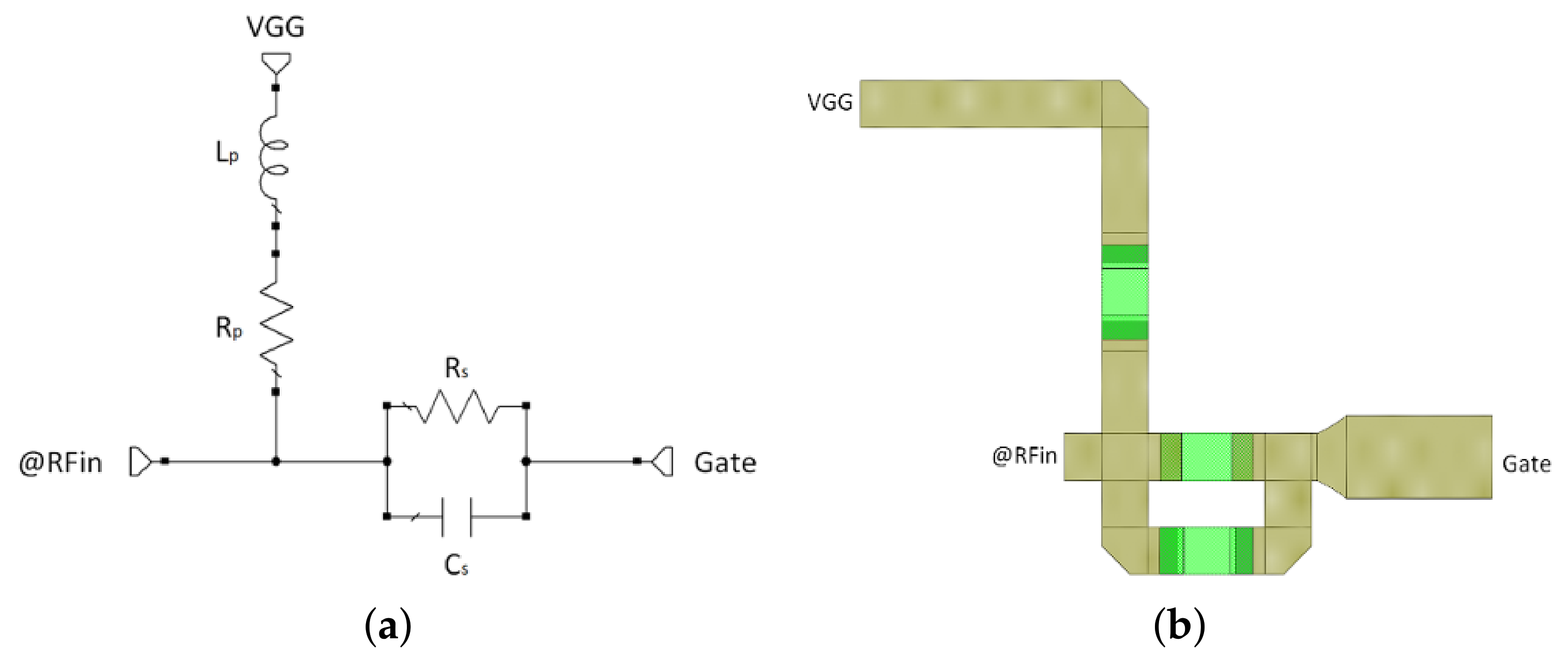
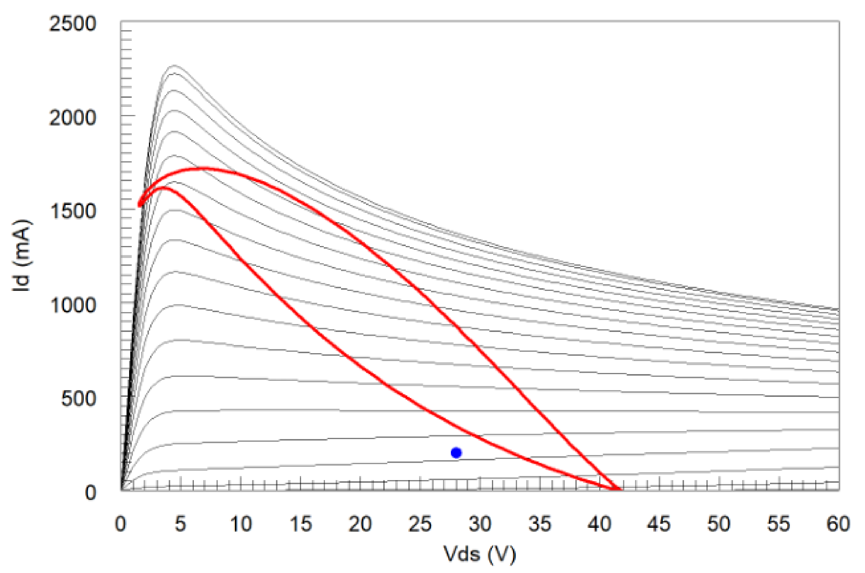
2.2. Bandwidth, Biasing and Stability Network

For the design of the power stage, the center frequency f 0 = 3.55 GHz with 300 MHz of bandwidth (8.4% of fractional bandwidth) has been adopted, while a class-AB bias condition with V D S = 28 V and I D = 200 mA ( V G S = −2.63 V) has been chosen. The quiescent current I D corresponds approximately to 10% of the maximum value (deep class AB), and it has been selected to fulfill the conditions for harmonic manipulation technique application [23].
Because the amplifier may show an impedance with a negative real part at a given section, and thus oscillates at some frequencies, a stability network has been designed and ultimately placed between the HEMT gate and the input matching network.
Consequently, the scheme reported in Figure 2a has been adopted, where the shunt R P resistor and the series parallel R S - C S network guarantee low-frequency and in-band stability conditions, respectively. Figure 2b shows the layout of the chosen stability network, where the inductor L P has been realized through a shorted transmission line with 0.8 mm width (characteristic impedance Z C = 23.3 Ω ), which is comparable with the widht of the 0603 SMD package used for the other passive components (resistors and capacitors).
From a theoretical point of view, the unconditional stability analysis of two-port microwave circuits can be performed in several ways, namely by the Rollet stability factor K and the scattering matrix determinant Δ [24,25], or by the geometric stability factors mu [26], or by the Nyquist criterion [27].
Figure 3 shows that a geometric stability factor greater than 1 between 0 and 14 GHz has been achieved ( R P = 17 Ω , L P = 3.1 nH, R S = 6.8 Ω , C S = 6.12 pF). In the same figure, a maximum transducer power gain (GMax) value of about 18 dB is outlined in the 3.0–4.0 GHz band, whereas GMax values with and without the stability network, are reported as well.

2.3. Input & Output Matching Network

Optimum load ( Γ o u t ) and source ( Γ i n ) reflection coefficients at the fundamental frequency have been found using source and load pull simulations. In this regard, load pull simulations are presented in Figure 4, where Pout and PAE contours at 3.4 GHz (a), 3.55 GHz (b) and 3.7 GHz (c), respectively, are outlined.
Next, ideal optimum input and output reflection coefficients ( Γ i n and Γ o u t ) at the fundamental frequency of 3.55 GHz are reported, both in values (Table 1) and in graphical form (Figure 5), whereas terminations up to the third harmonic have been defined using ideal tuners to maximize Pout, Gain and PAE of the whole amplifier.
It is worth to be noted that the optimum load is complex at the fundamental frequency of 3.55 GHz, since the output matching network has to transform the 50 Ω output load into a complex impedance, whereas the optimal loads are purely reactive at harmonic frequencies.
In order to synthesize the above defined optimum load values for the multi harmonic tuned PA, the impedance transforming properties of transmission lines have been used to implement input and ouput matching networks. In fact, the reactive matching method (single stub tuning) [28] has been used to design a reactive matching network for each harmonic.
According to this method, a series microstrip transmission line together with an open-circuited shunt stub can transform a 50-ohm, or any arbitrary load impedance, into the desired value of impedance. A general matching circuit schematic has been represented in Figure 6, where y L = 1 is the load normalized admittance ( Y L = 1 / 50 Siemens), y 1 = ± j · b 1 is the normalized admittance of the shunt open stub ( b 1 > 0 for capacitive susceptance, b 1 < 0 for inductive susceptance, b s always positive), and the length L 1 determines the value of ± j · b 1 . The addition of y 1 = ± j · b 1 to y L produces a motion along the unity constant-conductance circle from y L = 1 to y 2 = 1 ± j · b 1 . The series transmission line of length L 2 transforms y 2 into the desired normalized admittance y I N . As a consequence, the value of b 1 must be selected so that y 2 and y I N are on a constant | Γ | circle.
The designed output matching network is presented in Figure 7a, where the transmission line and open stub matching network that control each harmonic have been outlined ( f 0 = 3.55 GHz). A constant microstrip width of 0.8 mm has been adopted ( Z C = 23.3 Ω ). At first, the network has been designed with ideal transmission lines for each single frequency, then real microstrip elements have been introduced together with parasitic elements. Finally, the three matching networks have been assembled all together and the transmission line parameters have been optimized in order to achieve the desired impedance values.
Furthermore, the output matching network has been synthesized using a three-section structure, as shown in Figure 7b. The synthesized load at the matched port ( Z L ( n f ) ) and the loads presented across each section are reported in Figure 8 for the fundamental frequency (Figure 8a), the second (Figure 8b) and third (Figure 8c) harmonic, in a larger frequency range from 3.3 to 3.8 GHz. Section planes are placed in such a way that they properly explore how the correspondent synthesized load changes its value, according to the above described reactive matching method.
The synthesized input matching network is depicted in Figure 9a, where the fundamental harmonic ( f 0 = 3.55 GHz) has been controlled by a transmission line and an open stub, while another network has been designed and implemented for the control of both second and third harmonic simultaneously (the width of the 2nd and 3rd harmonic open stub is 0.24 mm, Z C = 46.3 Ω ). Such choice has led to a significant reduction of the amplifier dimensions.
Likewise the output matching network, the input matching network has been tested through three theoretical cutting in the whole structure, as shown in Figure 9b, whereas the actual loads at the matched port ( Z S ( n f ) ) and across each section are reported in Figure 10 for the fundamental frequency in the range 3.3–3.8 GHz, and the corresponding ranges for second and third harmonics.
Two capacitors acting as DC and low frequency signals block ( C o u t = 10 pF and C i n = 0.6 pF in Figure 7 and Figure 9, respectively), have been inserted into the matching networks.
Note that, in order to avoid electromagnetic coupling (cross-talk), the distance between two adjacent transmission lines was maintained always higher than 3 · H 0.8 mm, where H = 0.254 mm is the substrate thickness.
The synthesized input and output reflection coefficients ( Γ i n and Γ o u t ) are reported in the aforementioned Table 1 (value form) and Figure 5 (graphical form, red diamond symbol), where the comparison with the correspondent ideal loads shows a very good agreement.
The input-output matching networks have also been electromagnetically simulated with the Method of Moment (MoM) electromagnetic simulator AXIEM, available inside the AWR-MWO software by Cadence Design Systems. Electromagnetic simulations can evidence some parasitic or coupling mechanisms, which are not taken into account by the AWR circuit model components. However, no significant variations have been evidenced.
The schematic and the corresponding layout of the power amplifier are reported in Figure 11. Dimensions of the whole amplifier are 46 mm (lenght) and 14 mm (width).
Two biasing networks close to V G G and V D D pads made by capacitors and resistances, have been implemented in the final layout, to short circuit the RF signal and to reduce the eventual ripple in the bias voltages. The use of resistive components, in series with the larger capacitances in the biasing network, decreases the Q-factor of the latter, assuring an S 11 ( f ) close to the short circuit at baseband frequencies.
The simulated losses of the passive networks are shown in Figure 12. The output matching network losses are lower than 0.4 dB, whereas the input matching structure and the stability network display a total loss between 4 and 2 dB in the frequency range from 3.4 GHz to 3.7 GHz, with a slope to counteract the intrinsic negative slope introduced by the active device.
The intrinsic load curve (i.e., achieved across the intrinsic current source of the non linear HEMT model) at 1 dB compression point, alongside with the static bias point overlapped to the extrinsic output characteristics, are reported in Figure 13. It was demonstrated in [3] that the presence of the upper bending in the dynamic load line of a GaN HEMT, generates an output current waveform with a negative second harmonic current component. As a consequence, the fundamental and second harmonic currents are opposite in phase. This phase relation is mandatory, otherwise the use of an output second-harmonic termination becomes deleterious [16].
The nonlinear behaviour of the designed PA has been simulated focusing on intermodulation distorsion (IMD), AM-AM distortion and AM-PM conversion. The IMD performance has been simulated with a two tones input source with equal amplitude at two different frequency spacing, namely 10 MHz (Figure 14a) and 50 MHz (Figure 14b). In particular, at 33 dBm input power, third-order (IMD3) and fifth-order (IMD5) values are below −20 dB and −47 dB, respectively, for the 10 MHz tone spacing), and below −18 dB and −38 dB for the 50 MHz tone spacing, which underlines a good linearity performance. Similarly, the AM-AM distortion and AM-PM conversion have been simulated and reported in Figure 15 at the lower (3.4 GHz), center (3.55 GHz) and upper (3.7 GHz) frequency. At the nominal operating point (i.e., Pin = 33 dBm), they are lower than 6.5 dB and 5 degree, respectively.
The fabricated PA is shown in Figure 16, where two SMA connectors have been used to connect the amplifier to the RF source and the load.

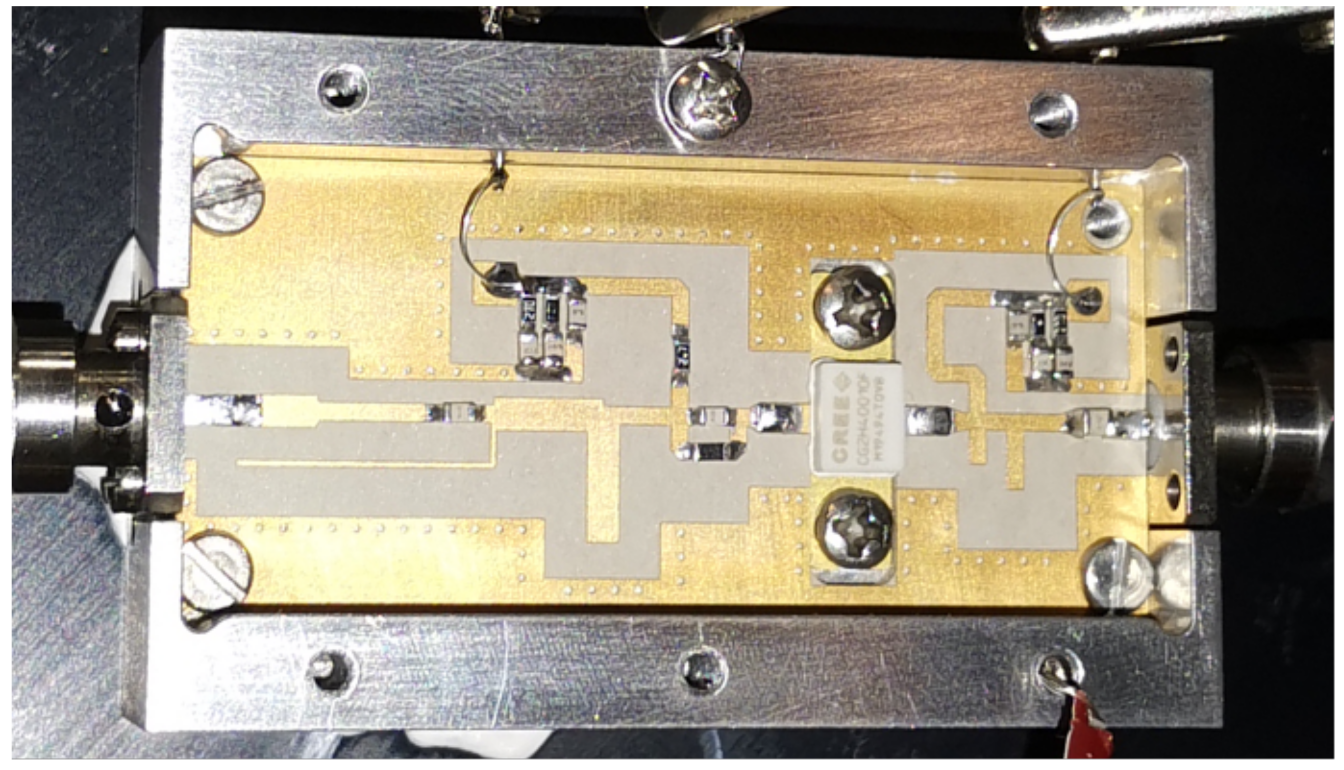
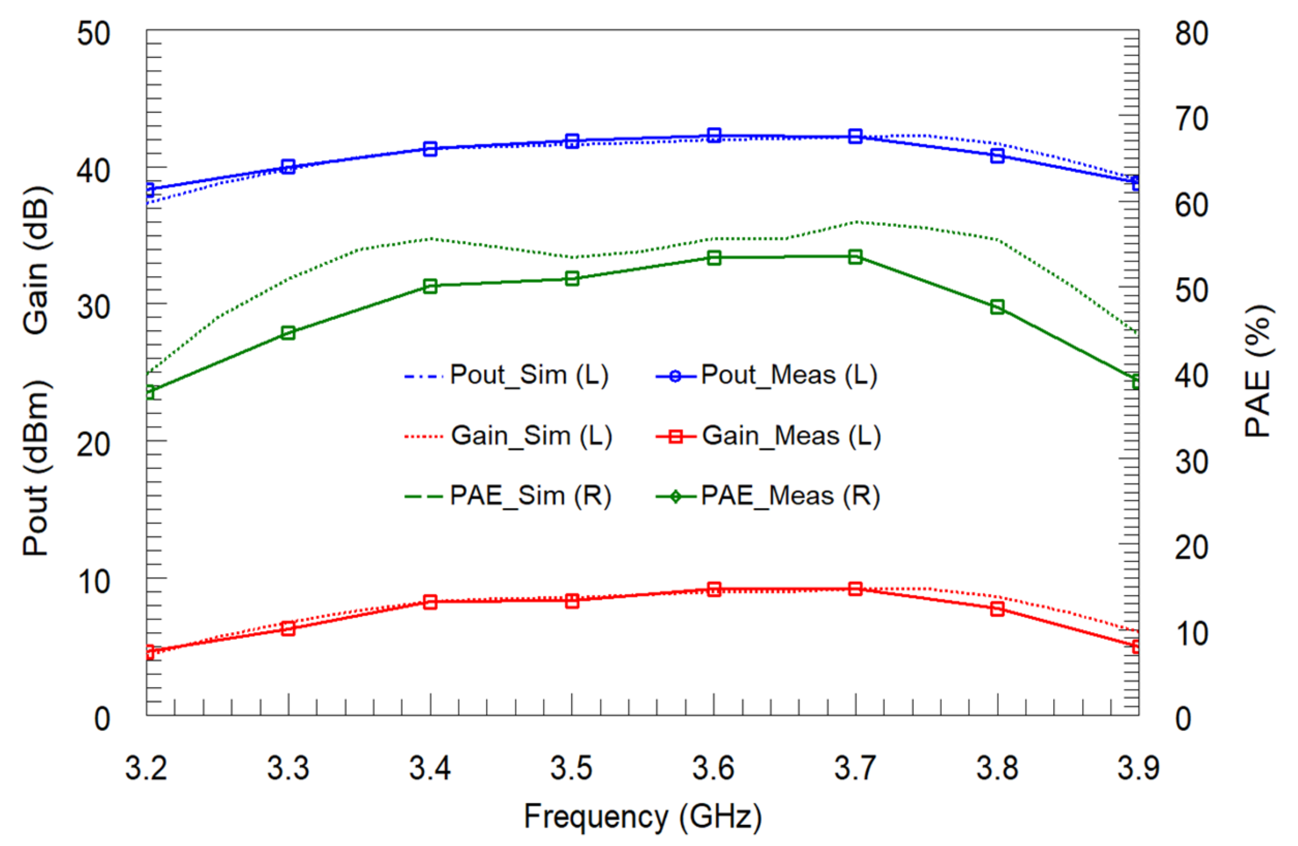
3. Experimental Results

The realized PA has been characterized by both linear and non-linear measurements. To define small-signal behavior, PA scattering parameters have been measured with a vector network analyzer.
Figure 17 shows the measured scattering parameters of the PA evaluated at the bias point ( V D S = 28 V, I D = 200 mA), together with the simulated ones. In simulation the dielectric constant of the substrate has been fixed to 11.2. A good agreement between simulations and measurements has been reported, particularly on S 21 magnitude in the working frequency band 3.4 GHz–3.7 GHz. As far as S 11 and S 22 are concerned, the difference between simulation and measurement can be ascribed to the input and output connector and to the weld parasitics. A small signal gain ( S 21 ) of 12.4 dB (with a ripple of 0.35 dB) was registered in the range from 3.4 GHz to 3.7 GHz, with an input and output reflection coefficients lower than −10 dB (input, S 11 ) and −7.3 dB (output, S 22 ), respectively, in the same frequency range.
To define large signal behavior in a continuous wave mode, PA parameters have been measured using a LabView controlled measurement system available at MECSA Tor Vergata University of Rome Labs. The system is based on a Signal generator and an Agilent E4448A spectrum analyzer.
Measured PA data at 3.4 GHz, 3.55 GHz and 3.7 GHz for the nominal bias condition ( I D = 200 mA, V D S = 28 V), and the comparison with simulated results (after reverse engineering models update) are reported in Figure 18), respectively. Moreover, measured PAE in the frequency range 3.2 GHz–3.8 GHz are depicted in Figure 19. A saturated output power Pout = 42.27 dBm with power gain GP = 9.3 dB and PAE = 53.5% (drain efficiency = 60%), were obtained at 3.7 GHz.
Next, the PA has been characterized in the frequency range from 3.2 to 3.9 GHz, with 33 dBm of fixed input available power, corresponding to the PAE peak. Results are reported in Figure 20 and compared with simulated counterparts. The achieved results show a ripple in the output power and power gain lower than 1 dB, and a PAE value higher than 45%, in the frequency range 3.3 GHz–3.8 GHz.
Comparisons of this PA performance with the state of the art of S band GaN PAs are reported in Table 2 (and showed in graphical form in Figure 21).

4. Conclusions

In this paper, the design and the physical realization of an S band multi harmonic tuned power amplifier in GaN technology and hybrid form have been presented. The proposed PA is in the band recently assigned to 5G systems, and it is based on a commercial CREE device, seldom used so far, according to the published papers. The focus of this work is on the design technique for the matching networks, where the Harmonic Tuning approach has been implemented. At the same time, the design stages have taken into account the amplifier dimension in its whole. The amplifier’s small and large signal performance have been shown and discussed. In an operating bandwidth of 300 MHz around f 0 = 3.55 GHz (8.4% of fractional bandwidth), experimental results demonstrate 42.3 dBm output power, 9.3 dB power gain and 53.5% PAE (60% drain efficiency) at 3.7 GHz. According to the authors’ knowledge, the values reported and documented in this paper are the best achieved until now with the chosen device, in terms of Pout and BW, which leads to place this article in the state of the art of power amplifier for 5G applications operating in the sub 6 GHz bandwidth.

Author Contributions

Conceptualization, S.G.; writing—original draft preparation, S.G. and S.P.; writing—review and editing, S.G. and P.C.; supervision, P.C. All authors have read and agreed to the published version of the manuscript.

Funding

This research received no external funding.

Institutional Review Board Statement

Not applicable.

Informed Consent Statement

Not applicable.

Conflicts of Interest

The authors declare no conflict of interest.

Abbreviations

The following abbreviations are used in this manuscript:
EMElectromagnetic
PAPower Amplifier
GaNGallium Nitride
IMNInput Matching Network
OMNOutput Matching Network

References

  1. Raab, F.; Asbeck, P.; Cripps, S.; Kenington, P.; Popovic, Z.; Pothecary, N.; Sevic, J.; Sokal, N. Power amplifiers and transmitters for RF and microwave. IEEE Trans. Microw. Theory Tech. 2002, 50, 814–826. [Google Scholar] [CrossRef] [Green Version]
  2. Prejs, A.; Wood, S.; Pengelly, R.; Pribble, W. Thermal analysis and its application to high power GaN HEMT amplifiers. In Proceedings of the 2009 IEEE MTT-S International Microwave Symposium Digest, Boston, MA, USA, 7–12 June 2009; pp. 917–920. [Google Scholar] [CrossRef]
  3. Colantonio, P.; Limiti, E.; Giannini, F. High Efficiency RF and Microwave Solid State Power Amplifiers; Wiley Series in Microwave and Optical Engineering; Wiley: Chichester, UK, 2009. [Google Scholar]
  4. Raab, F. Maximum efficiency and output of class-F power amplifiers. IEEE Trans. Microw. Theory Tech. 2001, 49, 1162–1166. [Google Scholar] [CrossRef]
  5. Colantonio, P.; Giannini, F.; Leuzzi, G.; Limiti, E. On the class-F power amplifier design. Int. J. Microw.-Comput.-Aided Eng. 1999, 9, 129–149. [Google Scholar] [CrossRef]
  6. Raab, F. Class-F power amplifiers with maximally flat waveforms. IEEE Trans. Microw. Theory Tech. 1997, 45, 2007–2012. [Google Scholar] [CrossRef]
  7. Raffo, A.; Vadalà, V.; Bosi, G.; Trevisan, F.; Avolio, G.; Vannini, G. Waveform engineering: State-of-the-art and future trends (invited paper). Int. J. Microw.-Comput.-Aided Eng. 2017, 27, e21051. [Google Scholar] [CrossRef] [Green Version]
  8. Liu, G.; Li, S.; Cheng, Z.; Feng, H.; Dong, Z. High-efficiency broadband GaN HEMT power amplifier based on harmonic-tuned matching approach. Int. J. Microw.-Comput.-Aided Eng. 2020, 30, e22097. [Google Scholar] [CrossRef]
  9. Olavsbråten, M.; Mathiesen, T.; Berry, E. Design of an efficient wideband (1–5GHz) 10W PA in GaN technology using harmonic tuning. In Proceedings of the 2017 IEEE 18th Wireless and Microwave Technology Conference (WAMICON), Cocoa Beach, FL, USA, 24–25 April 2017; pp. 1–5. [Google Scholar] [CrossRef]
  10. Colantonio, P.; Giannini, F.; Giofre, R.; Limiti, E.; Serino, A.; Peroni, M.; Romanini, P.; Proietti, C. A C-band high-efficiency second-harmonic-tuned hybrid power amplifier in GaN technology. IEEE Trans. Microw. Theory Tech. 2006, 54, 2713–2722. [Google Scholar] [CrossRef] [Green Version]
  11. Li, S.; Lin, V.C.; Nandhasri, K.; Ngarmnil, J. New high-efficiency 2.5 V/0.45 W RWDM class-D audio amplifier for portable consumer electronics. IEEE Trans. Circuits Syst. I Regul. Pap. 2005, 52, 1767–1774. [Google Scholar] [CrossRef]
  12. Dooley, J.; Farrell, R. A Practical Class S Power Amplifier for High Frequency Transmitters. In Proceedings of the Royal Irish Academy Colloquium on Emerging Trends in Wireless Communications 2008, Dublin, Ireland, 23–24 April 2008. [Google Scholar]
  13. Sokal, N. Class E high-efficiency power amplifiers, from HF to microwave. In Proceedings of the 1998 IEEE MTT-S International Microwave Symposium Digest (Cat. No.98CH36192), Baltimore, MD, USA, 7–12 June 1998; Volume 2, pp. 1109–1112. [Google Scholar] [CrossRef]
  14. Abbasian, S.; Johnson, T. Effect of Second and Third Harmonic Input Impedances in a Class-F Amplifier. Prog. Electromagn. Res. C 2015, 56, 39–53. [Google Scholar] [CrossRef] [Green Version]
  15. Li, X.; Colantonio, P.; Giannini, F.; Yu, H.; Lin, C. S-Band Class-C-F Power Amplifier with 2nd Harmonic Control at the Input. Appl. Sci. 2020, 10, 259. [Google Scholar] [CrossRef] [Green Version]
  16. Colantonio, P.; Giannini, F.; Leuzzi, G.; Limiti, E. Multiharmonic manipulation for highly efficient microwave power amplifiers. Int. J. Microw.-Comput.-Aided Eng. 2001, 11, 366–384. [Google Scholar] [CrossRef]
  17. Colantonio, P.; Giannini, F.; Leuzzi, G.; Limiti, E. Very high efficiency microwave amplifier. The harmonic manipulation approach. In Proceedings of the 13th International Conference on Microwaves, Radar and Wireless Communications. MIKON-2000, Conference Proceedings (IEEE Cat. No.00EX428). Wroclaw, Poland, 22–24 May 2000; Volume 3, pp. 33–46. [Google Scholar] [CrossRef]
  18. Smith, R.; Glynn, S.; Greene, J.; Devlin, L. A Fully Integrated 3.5 GHz Single Chip GaN Doherty PA for sub-6 GHz 5Ge. 2019. Available online: https://www.rfglobalnet.com/doc/a-fully-integrated-ghz-single-chip-gan-doherty-pa-for-sub-ghz-g-0001 (accessed on 4 July 2021).
  19. Global Mobile Supplier Association Spectrum for Terrestrial 5G Networks: Licensing Developments Worldwide. 2019. Available online: http://comitatomcs.eu/wp-content/uploads/2019/08/190730-GSA-5G-spectrum-report-July.pdf (accessed on 22 July 2021).
  20. Barret, J. 5G Spectrum Bands. 2017. Available online: https://gsacom.com/5g-spectrum-bands/ (accessed on 22 July 2021).
  21. Pengelly, R.S.; Wood, S.M.; Milligan, J.W.; Sheppard, S.T.; Pribble, W.L. A Review of GaN on SiC High Electron-Mobility Power Transistors and MMICs. IEEE Trans. Microw. Theory Tech. 2012, 60, 1764–1783. [Google Scholar] [CrossRef]
  22. Pisa, S.; Chicarella, S.; Cusani, R.; Citrolo, J. 30–512 MHz power amplifier design using GaN transistor. Microw. Opt. Technol. Lett. 2018, 60, 1280–1286. [Google Scholar] [CrossRef]
  23. Colantonio, P.; Giannini, F.; Leuzzi, G.; Limiti, E. Theoretical facet and experimental results of harmonic tuned PAs. Int. J. Microw.-Comput.-Aided Eng. 2003, 13, 459–472. [Google Scholar] [CrossRef]
  24. Rollett, J. Stability and Power-Gain Invariants of Linear Twoports. IRE Trans. Circuit Theory 1962, 9, 29–32. [Google Scholar] [CrossRef] [Green Version]
  25. Woods, D. Reappraisal of the unconditional stability criteria for active 2-port networks in terms of S parameters. IEEE Trans. Circuits Syst. 1976, 23, 73–81. [Google Scholar] [CrossRef]
  26. Edwards, M.; Sinsky, J. A new criterion for linear 2-port stability using a single geometrically derived parameter. IEEE Trans. Microw. Theory Tech. 1992, 40, 2303–2311. [Google Scholar] [CrossRef]
  27. Pisa, S.; Zolesi, M. A method for stability analysis of small-signal microwave amplifiers. Int. J. Microw.-Comput.-Aided Eng. 1998, 8, 293–302. [Google Scholar] [CrossRef]
  28. Gonzalez, G. Microwave Transistor Amplifiers: Analysis and Design, 2nd ed.; Prentice-Hall, Inc.: Hoboken, NJ, USA, 1996. [Google Scholar]
  29. Drews, S.; Rautschke, F.; Maassen, D.; Nghe, C.T.; Boeck, G. A 10-W S-band power amplifier for future 5G communication. In Proceedings of the 2017 47th European Microwave Conference (EuMC), Nuremberg, Germany, 1–10 October 2017; pp. 152–155. [Google Scholar] [CrossRef]
  30. Duffy, M.R.; Berry, E.; Lasser, G.; Popović, Z. An Efficient Linearized Octave-Bandwidth Power Amplifier for Carrier Aggregation. In Proceedings of the 2018 IEEE/MTT-S International Microwave Symposium-IMS, Philadelphia, PA, USA, 10–15 June 2018; pp. 473–476. [Google Scholar] [CrossRef]
  31. Smith, R.; Devlin, L.; Tran, K.; Martin, R. An Adaptable GaN Power Amplifier for S-Band Radar. 2021. Available online: https://www.prfi.com/wp-content/uploads/2019/10/An-Adaptable-GaN-Power-Amplifier-for-S-Band-Radar.pdf (accessed on 22 July 2021).
  32. Liu, C.; Li, X.; Zhao, Y.; Qi, T.; Du, X.; Chen, W.; Ghannouchi, F.M. Investigation of High-Efficiency Parallel-Circuit Class-EF Power Amplifiers With Arbitrary Duty Cycles. IEEE Trans. Ind. Electron. 2021, 68, 5000–5012. [Google Scholar] [CrossRef]
  33. Zhou, L.H.; Zhou, X.Y.; Chan, W.S.; Sharma, T.; Ho, D. Wideband Class-F-1 Power Amplifier With Dual-Quad-Mode Bandpass Response. IEEE Trans. Circuits Syst. I Regul. Pap. 2020, 67, 2239–2249. [Google Scholar] [CrossRef]
  34. Ochoa-Armas, D.; Lavandera-Hernández, I.; Fernández-Ramón, D.; Loo-Yau, J.R.; Molina-Ceseña, M.; Pérez-Wences, C.; Hernández-Domínguez, E.A.; Reynoso-Hernández, J.A.; Moreno, P. A nonlinear empirical I/V model for GaAs and GaN FETs suitable to design power amplifiers. Int. J. Microw.-Comput.-Aided Eng. 2021, 31, e22552. [Google Scholar] [CrossRef]
  35. Abdurrakhman Hamid, A.; Alam, B.R. Power Amplifier Design in Broadband RF IC Transponder for Manufacture 4.0 RF Link. In Proceedings of the 2019 International Symposium on Electronics and Smart Devices (ISESD), Badung, Indonesia, 8–9 October 2019; pp. 1–4. [Google Scholar] [CrossRef]
  36. Góralczyk, M. A 3.4 to 3.8 GHz 45 W Inverted 3-Way Doherty Power Amplifier. In Proceedings of the 2020 23rd International Microwave and Radar Conference (MIKON), Warsaw, Poland, 5–8 October 2020; pp. 420–423. [Google Scholar] [CrossRef]
  37. Zhao, Y.; Li, X.; Gai, C.; Du, X.; Helaoui, M.; Ghannouchi, F. Optimal Fundamental Load Modulation for Class-X Harmonically Tuned Power Amplifier. In Proceedings of the 2019 IEEE Asia-Pacific Microwave Conference (APMC), Hong Kong, China, 15 May 2019; pp. 1649–1651. [Google Scholar] [CrossRef]
Figure 1. Matching networks of an HT PA.
Electronics 10 02318 g001
Figure 2. Stability network scheme (a) and layout realization (b).
Electronics 10 02318 g002
Figure 3. Effect of the stability network on maximum transducer power gain (GMax) and geometric stability factor (mu).
Electronics 10 02318 g003
Figure 4. Load pull simulations at 3.4 GHz (a), 3.55 GHz (b) and 3.7 GHz (c).
Electronics 10 02318 g004
Figure 5. Optimum input (a) and output (b) harmonic loads, set them up with ideal tuners (circle symbols) and currently synthesized (diamond symbols).
Electronics 10 02318 g005
Figure 6. Reactive matching scheme.
Electronics 10 02318 g006
Figure 7. Output matching network: transmission line and open stub controlling each harmonic (a), and section planes used to synthesized the whole structure (b).
Electronics 10 02318 g007
Figure 8. Output matching network: synthesized load at the matched port and across each matching network section, for the fundamental frequency in the range 3.3–3.8 GHz (a), and the corresponding second (b) and the third harmonics (c).
Electronics 10 02318 g008
Figure 9. Input matching network: transmission line and open stub controlling each harmonic (a), and section planes used to synthesized the whole structure (b).
Electronics 10 02318 g009
Figure 10. Input matching network: synthesized load at the matched port and across each matching network section, for the fundamental frequency in the range 3.3–3.8 GHz (a), and the corresponding ranges for second (b) and third harmonics (c).
Electronics 10 02318 g010
Figure 11. Schematic (a) and layout (b) of the power amplifier.
Electronics 10 02318 g011
Figure 12. Losses of input (a) and output (b) matching networks.
Electronics 10 02318 g012
Figure 13. Simulated intrinsic load curve at 1 dBcp.
Electronics 10 02318 g013
Figure 14. Two–tone IMD simulations: (a) 10 MHz and (b) 50 MHz of tone spacing, center frequency 3.55 GHz.
Electronics 10 02318 g014
Figure 15. Simulated AM–AM and AM–PM for the carrier frequency of 3.4 GHz (lower frequency), 3.55 GHz (center frequency) and 3.7 GHz (upper frequency).
Electronics 10 02318 g015
Figure 16. Photo of the realized PA.
Electronics 10 02318 g016
Figure 17. PA linear performance.
Electronics 10 02318 g017
Figure 18. Power amplifier performance at 3.4 GHz (a), 3.55 GHz (b) and 3.7 GHz (c).
Electronics 10 02318 g018
Figure 19. Measured PAE values in the frequency range 3.2 GHz–3.8 GHz.
Electronics 10 02318 g019
Figure 20. PA performance at Pin = 33 dBm.
Electronics 10 02318 g020
Figure 21. State of the art of GaN PAs in graphical form.
Electronics 10 02318 g021
Table 1. Optimum input and output harmonic load values.
Freq. (GHz) Γ in Γ out
IdealSynthesizedIdealSynthesized
3.55 0.933 e j · 158 0.933 e j · 157 . 6 0.664 e j · 173 0.664 e j · 172 . 8
7.1 1 e j · 110 0.980 e j · 108 . 2 1 e j · 172 0.994 e j · 169 . 7
10.65 1 e j · 38 0.945 e j · 37 . 15 1 e j · 141 0.962 e j · 137 . 6
Table 2. State of the art of GaN PAs.
Ref.YearFreq (GHz) BW % (%)Pout (dBm)PAE(%)Gain (dB)
[9]20173.713340.746.810
[29]20173.575404810.5
[30]20183.56741.747.59
[31]20193.51243.452.614
[32] 1 20203.73386110
[33]20203.6738.55212.8
[34]20213.6NA39.9527.2
[35] 1 , 2 20192.44.139.450NA
[36] 1 , 3 20203.71146.662.66.5
[37] 1 20190.8NA426414
T.W.20213.78.442.353.59.3
1 Same device. 2 Simulations only. 3 Doherty, 3 devices.
Publisher’s Note: MDPI stays neutral with regard to jurisdictional claims in published maps and institutional affiliations.

