Article

Theory and Design of a Flexible Two-Stage Wideband Wilkinson Power Divider

by
Antra Saxena
1,*,†,
Mohammad Hashmi
2,
Deepayan Banerjee
1 and
Muhammad Akmal Chaudhary
3
1
Department of Electronics and Communication Engineering, Indraprastha Institute of Information Technology Delhi, New Delhi 110020, India
2
Department of Electrical and Computer Engineering, School of Engineering and Digital Sciences, Nazarbayev University, Nur-Sultan 010000, Kazakhstan
3
Department of Electrical and Computer Engineering, College of Engineering and Information Technology, Ajman University, Ajman, United Arab Emirates
*
Author to whom correspondence should be addressed.
Current address: R & D Block, Indraprastha Institute of Information Technology Delhi, New Delhi 110020, India.
Electronics 2021, 10(17), 2168; https://doi.org/10.3390/electronics10172168
Submission received: 11 July 2021 / Revised: 24 August 2021 / Accepted: 28 August 2021 / Published: 5 September 2021
(This article belongs to the Section Microwave and Wireless Communications)

Abstract

:
This article presents the design scheme of a wideband Wilkinson Power Divider (WPD) with two-stage architecture utilizing quarter-wave transmission lines and short-circuit stubs. The bandwidth of the proposed WPD is flexible and can be controlled using the design parameters. The proposed design achieves excellent isolation between output ports in addition good in-band performance. The analysis of the proposed circuit results in a simplified transfer function which is then equated with a standard band-pass transfer function to determine the parameters of transmission lines, stub’s impedances, and the value of the isolation resistors. Furthermore, it is also demonstrated that a simple alteration in the proposed circuit enables the design of a wideband DC isolated WPD that maintains a good in-band and isolation performance. A number of case studies have been included to highlight the flexibility of the proposed design. Two distinct prototypes are developed on different boards to demonstrate the wideband performance of the proposed design. An excellent agreement between the experimental and measured results for both the designs over a wide band including very good isolation between ports validate the proposed design.

1. Introduction

The advancements in communication protocols and standards have led to a number of innovations in both active and passive circuits, components and devices [1,2,3,4]. Within the passive components regime, there have been a plethora of design reports on advanced configurations for power divider, impedance transformer, directional coupler etc. In the context of power dividers, the T-junction configuration can be considered the most fundamental but it is constrained by poor isolation between the output ports. The isolation issues are readily addressed by Wilkinson Power Divider (WPD) [5]. The WPD achieves good matching at the ports and exhibits excellent isolation between the output ports. However, the WPD in its original form makes use of quarter-wavelength transmission line that limits the intrinsic bandwidth at a single frequency. Nonetheless, there have been extensive advancements in the WPD design techniques to meet the requirements of multi-standard communication systems. A majority of the research focus in the last decade has largely been on multi-band [6,7,8,9,10,11,12,13,14,15,16,17,18,19,20,21,22] and broadband WPDs [23,24,25,26,27,28,29,30,31,32,33,34,35,36,37,38,39,40,41,42,43,44,45,46,47,48,49,50,51,52,53,54,55,56,57,58].
A survey of the literature related to recent reports on WPD design reveals that the emphasis has been on enhancing the number of bands and isolation bandwidth [6,7,8,9,10,11,12,13,14,15,16,17,18,19,20,21,22]. There are number of techniques to increase the number of bands in the operating frequency range. Originally, the dual-band WPDs [6,7,8,9,10,11,12,13,14,15,16,17,18] evolved, later followed by tri-/quad-band WPDs [19,20,21,22]. However, the increase in the number of bands lead to increased circuit size along with circuit complexity. The dual-band WPDs in the literature include WPD without reactive elements namely by attaching two central transmission line stubs in the conventional structure [6], unequal WPD operating at arbitrary dual-frequencies [7], WPD with composite left-/right-handed transmission lines [8], WPD with high power division operating at two bands by cascading dual-band T-section structures [9], with reactive elements including two-transmission lines and reactive lumped elements [10], WPD without stubs and additional lumped elements [11], WPD with common inductor with complex load [12], coupled-line based WPD and including four lumped elements [13], multi-band WPD utilizing multi-section LC-ladder circuits [14], with extended frequency ratios including two-section two resistor WPD with design able frequency ratio from 1 to [15], coupled lines and open stubs based to provide compensation [16], an enhanced frequency ratio coupled-line dual-band WPD with different ratios [17], theory of different frequency ratio is presented by selecting different physical lengths ratio [18] and many more. Few tri-band WPDs includes, WPD operating at three bands with open-short circuit stubs at the input and output port [19], WPD operating at three frequencies utilizing λ /4 open stubs with less frequency bandwidth in the operating bands [20], tri-band WPD utilizing coupled-lines [21], and quad-band WPD using generalized negative-refractive-index transmission-line unit cells [22] etc.
Another solution lies in developing WPD design schemes for wideband operations. There are number of techniques to design wideband WPD by integrating dual-operation of filtering and frequency selectivity at single/multi-band simultaneously [23,24,25,26,27,28,29,30,31]. The different methods to design filtering WPDs include replacing the quarter-wave transmission line with the bandpass filter [23,24], merging the filtering and divider circuits to obtain the desired operation [25], etc. The few examples for designing these WPDs include the use of resonators such as spiral resonators to realize compact size and bandpass filtering response [26], filtering WPD based on four quarter-wave resonators to improve out-of-band rejection [27], replacing quarter-wave transmission line with multi-mode resonators capable of splitting the power and selecting the frequency simultaneously [28], filtering power divider with five resonators to enhance the second harmonic suppression [29], combination of WPD and Gysel PD to enhance out-of-band rejection [30], dual- wideband with filtering characteristics [31] and many more. These techniques provide dual-operation but suffers the disadvantage of narrow passband at the centre frequency, hence restricted their usage in ultra-wideband applications.
Hence, another technique was proposed to increase the passband of WPDs to provide power splitting at a wider range of operation [32,33,34,35,36,37,38,39,40,41,42,43,44,45,46,47,48,49,50,51,52,53,54,55,56,57,58]. These approaches essentially entail the increment of the operating bandwidth along with enhanced isolation between the output ports. One such technique to extend the operating bandwidth is multi-layer microstrip-to-slot-line transition [23,24,25,26,27,28,29,30,31,32,33,34,35,36,37,38]. These techniques include design of WPD with multilayer slotline with isolation resistor present between two layers [32], multilayer balanced-to-unbalanced PD with three metallic layers and two substrate layers [33], WPD based on slotline resonators with two layer substrate [34], WPD using stepped impedance three-line coupled structure [35], out-of-phase PDs using tightly coupled lines and slotline transitions [36], out-of-phase WPD based on slotline [37], out-of-phase PD based on double-sided parallel strip-lines [38], etc. However, these circuits are not practical for applications that require heat sinks because of two-layer substrate such as power amplifier. Other broadband WPD design techniques are built around multi-mode resonators [39,40,41], parallel-coupled lines [42,43,44] or quasi-coupled line based design [45], three-line coupled lines [46,47,48,49,50], multi-section WPDs [51], stepped impedance lines with open-circuited stubs [52,53], DC isolated wideband WPD with coupled lines at the input and output port with WPD core [54]. Although many of these techniques provide proper port matching and isolation between output ports, they include complicated design procedure and lack of appropriate analysis for the design of isolation network. Furthermore, the use of reactive lumped components in the isolation network restricts the usefulness of reported wideband WPDs in many emerging applications [55,56,57,58]. Another important design aspect along with wideband operation is the DC blocking capability which is extremely useful for balanced and Doherty power amplifiers etc. The WPD with DC-blocking capability either utilizes resonators, coupling structures, stepped-impedances, etc. Here, a two-stage quarter-wave transmission line WPD including DC blocking capability is proposed. The prominent characteristics of the proposed WPD are listed below:
  • Simple and generalized mathematical analysis.
  • Fully Resistive isolation network.
  • Closed-form equations for determining the value of isolation resistor without involving optimization.
  • Flexible transmission bandwidth.
  • Good isolation between two ports along with excellent port matching.
  • Ready scalability for DC blocking application.
Several case studies are also included to show the versatility of the proposed technique. Two prototypes are developed using the proposed approach which provides a very good agreement between the simulated and measured results.
This paper begins with Section 2 discussing and analyzing the WPD in detail followed by Section 3 including case studies and results. Section 4 describes a WPD with DC isolation capability and its mathematical derivations. The fabrication and measurement results are also discussed, followed by Section 5, which concludes the paper.

2. Analysis of Proposed Power Divider

Figure 1 is a depiction of the proposed wideband WPD. It consists of two transmission lines, short-circuit stubs, and two isolation resistors. The main advantage of using short-circuit stubs is, simple structure with excellent ultra-wideband performance and reduced complexity in circuit fabrication. Apparently, it is a symmetrical network and hence can be split in two halves along the line of symmetry. As a consequence, the proposed WPD can be analyzed using the standard odd- and even-mode techniques. The overall S-parameters can then be obtained from the respective even- and odd-mode S-parameters considering that they are related as S 11 = S 11 e , S 22 = S 33 = ( S 22 e + S 22 o )/2 and S 23 = ( S 22 e S 22 o )/2, where, S 11 e , S 22 e and S 22 o are parameters of even and odd-mode circuits, respectively, [59]. Here, subscript “o” and “e” refer to the odd- and even-mode parameters, respectively.

2.1. Even-Mode Analysis

Figure 2 represents the even-mode half circuit of the proposed wideband WPD. It is well known that a two-port asymmetrical network with load Z L (here Z S ) and source Z S (here 2 Z S ) is characterized in terms of ABCD parameters and its associated scattering matrix in (1a) and (1b).
S 11 = A Z L + B C Z S Z L D Z S A Z L + B + C Z S Z L + D Z S
S 21 = 2 Z S Z L A Z L + B + C Z S Z L + D Z S
The overall ABCD matrix of the even-mode circuit shown in Figure 2 can be calculated by multiplying the individual ABCD parameters of the transmission lines and the stubs. Here A A , B A , C A , D A and A B , B B , C B , D B are the elements of the ABCD matrices of lines Z A and Z B , respectively, while A S 1 , B S 1 , C S 1 , D S 1 and A S 2 , B S 2 , C S 2 , D S 2 are that of the short circuit stubs as expressed in (2a) and (2b), respectively. This can be simplified to deduce the ABCD parameters, using (3) and (4), for the even-mode circuit.
A a B a C a D a = cos θ j Z a sin θ j sin θ / Z a cos θ
where a = A, B
A S x B S x C S x D S x = 1 0 j cos θ / Z S x 1
where x = 1, 2
A c a s B c a s C c a s D c a s = A S 1 B S 1 C S 1 D S 1 A A B A C A D A × A B B B C B D B A S 2 B S 2 C S 2 D S 2
A c a s = cos 2 θ + Z A cos 2 θ sin θ Z S 2 + Z B cos 2 θ sin θ Z S 2 Z A sin 2 θ Z B
B c a s = j Z A cos θ sin θ + j Z B cos θ sin θ
C c a s = j sin θ cos θ Z A j cos 3 θ Z S 1 j cos 3 θ Z S 2 j Z A sin θ cos 3 θ Z S 1 Z S 2 + j Z B sin 2 θ cos θ Z A Z S 1 j Z B cos 3 θ sin θ Z S 1 Z S 2 + j sin θ c o s θ Z B + j Z A cos θ sin 2 θ Z S 1 Z B
D c a s = cos 2 θ + Z A cos 2 θ sin θ Z S 1 Z B sin 2 θ cos θ Z A + Z B cos 2 θ sin θ Z S 1
where A c a s , B c a s , C c a s , D c a s are the elements of the overall cascaded ABCD matrix. The filtering characteristics of the circuit can be obtained by amplitude squared transfer function, S 21 given in (5). Here, impedance transformation ratio is p = Z L / Z S with p 1 (with, load impedance Z S and source impedance 2 Z S ). From (1a) and (1b), F W P D is given by (6). Based on (4) and (6), the F W P D can be calculated in terms of design parameters expressed in (7) and simplified in (8). The transfer characteristics of the proposed network is plotted as function of electrical length in Figure 3 with different values of impedances within the fabricable range of 20–150 Ω . The transfer characteristic as a function of S 21 and electrical length θ is plotted to illustrate its filtering response which can be compared to other filters.
| S 21 W P D | 2 = 1 1 + | F W P D | 2
where F W P D = S 11 / S 21
F W P D = A c a s + B c a s p C c a s p D c a s 2 p
F n e t w o r k = ( A 2 c o s 2 θ + A 1 + B 1 c o s θ p C 3 c o s 3 θ p C 1 c o s θ k D 2 c o s 2 θ k D 1 ) / 2 p
F n e t w o r k = ( p C 3 c o s 3 θ + ( A 2 p D 2 ) c o s 2 θ + ( B 1 p C 1 ) c o s θ + ( A 1 p D 1 ) / 2 p
From Figure 3, it can be noted that the characteristics is similar to a band pass filter and hence it can be compared with any theoretical band pass filter namely Chebyshev or Butterworth filter to determine the characteristic impedances of transmission lines and stubs. The Chebyshev bandpass filter transfer function is chosen here due to its fast roll-off speed compared to other filter functions. The impedances of transmission line and stubs are determined by comparing the transfer function of the proposed network with the theoretical Chebyshev transfer function F C H , where ε is the equal ripple factor, given in (9). Here, the transfer function F C H is represented by (10) [60] where T n + 1 is Chebyshev polynomial of degree n, x = c o s θ , x c = c o s θ c . The term θ c is defined as the electrical length at lower cut-off frequency [60]. For n = 2, Chebyshev polynomial T n + 1 are T 3 = 4 x 3 3 x and T 1 = x. Representing (10) in terms of x, x c , T 3 and T 1 , the expression in (10) results in (11).
| S 21 ( C H ) | 2 = 1 1 + ε 2 | F C H | 2
F C H = ( 1 + 1 x c 2 ) T n + 1 ( x x c ) ( 1 1 x c 2 ) T n 1 ( x x c ) 2 1 x 2
F C H = 4 ( 1 + sin 2 θ c ) cos 3 θ cos 3 θ c ( 4 2 sin θ c ) cos θ cos θ c 2 sin θ
The transmission characteristics S 21 of the Chebyshev function in (11) is plotted as function of θ and θ c in Figure 4. It is noted that at θ = 90 , the filter has band-pass characteristics with a change in bandwidth for different values of θ c .
To calculate the design parameters of the network, | S 21 W P D | 2 = | S 21 ( C H ) | 2 should be maintained and this essentially entails that | F W P D | = ε | F C H | . The resultant design equations are presented in (12) below.
p C 3 2 p = ε 4 ( 1 + sin 2 θ c ) 2 sin θ cos 3 θ c
A 2 p D 2 = 0
B 1 p C 1 2 p = ε 4 2 sin θ c 2 sin θ cos θ c
A 1 p D 1 = 0
Here, the electrical length θ of each element is 90 . The value of Z A , Z B , Z S 1 and Z S 2 can be calculated from (12) using MATLAB, for different values of transformation ratio p, ripple factor ε and θ c .
The values of the isolation resistors are also a critical design parameter. These are obtained in the next section from the odd-mode half-circuit analysis.

2.2. Odd-Mode Analysis

The odd-mode circuit half-circuit is depicted in Figure 5. It facilitates the conditions for calculating the values of resistors R 1 and R 2 . It is evident that the electrical length of transmission line and stubs are 90 , hence the impedance at node X remains at short-circuit resulting in the modified odd-mode circuit shown in Figure 6. For maintaining the conditions of perfect matching, the odd-mode half-circuit impedance Z o u t should be perfectly matched with output port impedance Z S . It should be noted that the line with the characteristics, impedance Z B is a quarter-wave transmission line with load R 1 /2. Here, Z Z is the impedance at node Z. Solving (13b), the relation between resistors R 1 and R 2 is obtained and provided in (14). The impedance parameters and isolation resistor values for wideband WPD with different θ c is tabulated in Table 1.
Z Z = ( Z B ) 2 R 1 / 2
Z o u t = Z Z R 2 / 2 = Z S
R 1 = 1 Z S ( 2 Z B 2 ( 4 Z S Z B 2 ) R 2 )
For different values of Z B , (14) results in distinct sets of isolation resistor combinations. Figure 7 represents the variation of resistors for different values of Z B (for different values of θ c ) listed in Table 1.

2.3. Design Steps

The procedure for designing wideband power divider can be compiled below as:
  • Choose the center frequency f c .
  • Divide the network designed using transmission lines and short-circuit stubs into half-circuit because of the symmetrical structure.
  • Perform the even-mode analysis to determine the impedance values, Z A , Z B , Z S 1 and Z S 2 according to (12) at centre frequency for distinct θ c .
  • Perform the odd-mode analysis to determine the values of the isolation resistors from (14).
  • For EM simulation and eventually layout, model the junction discontinuities properly using tapers and bends.

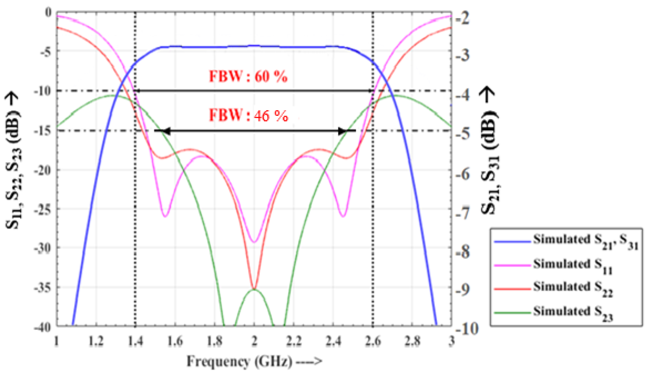
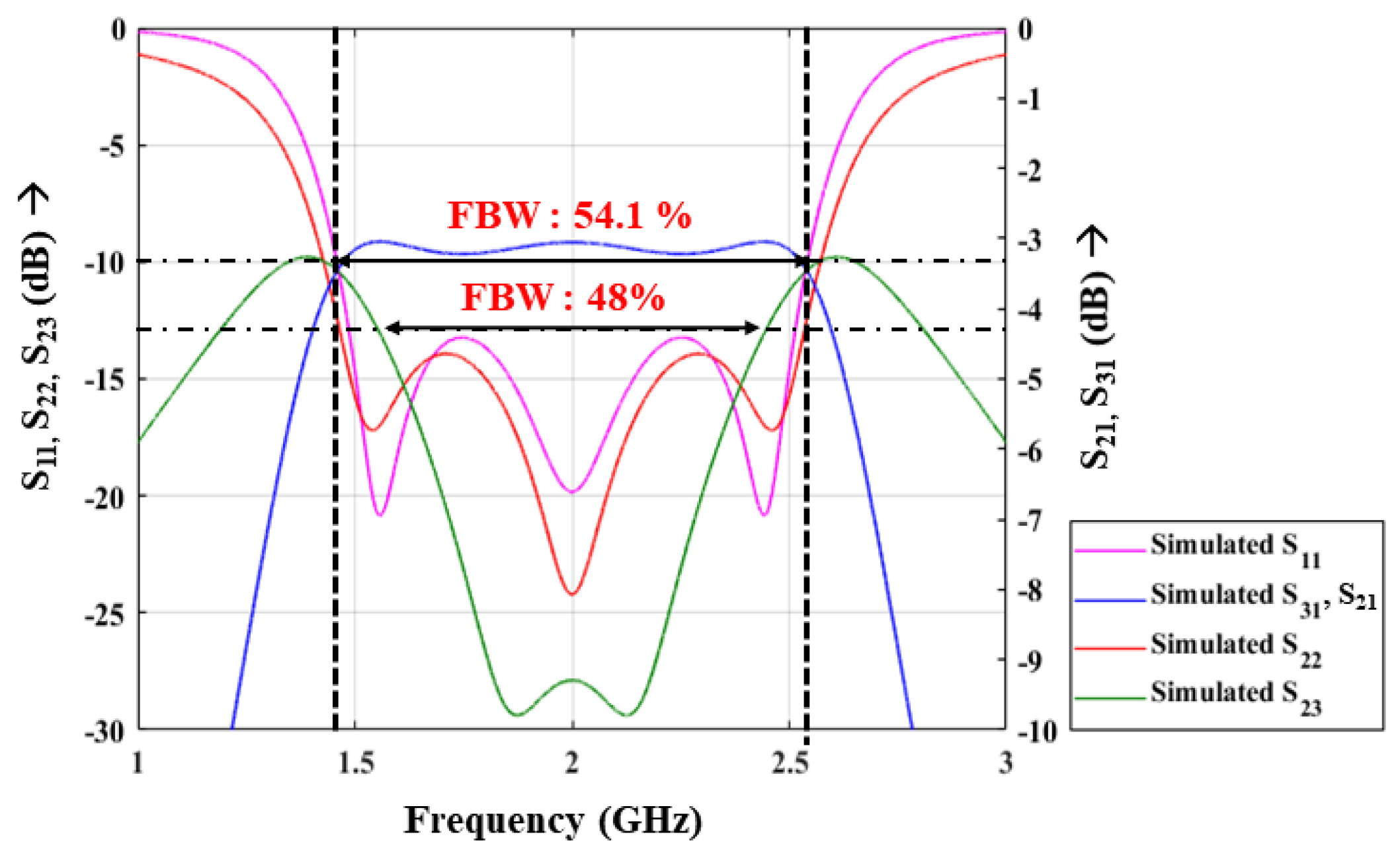
3. Case Studies, Results and Analysis

Based on the above design procedure and calculated design parameters listed in Table 1, simulation results of different case studies are presented in Figure 8, Figure 9 and Figure 10 illustrating S-parameters for varying θ c . It can be noted from the simulation results that, with increasing value of θ c , bandwidth of power divider decreases. The prototype shown in Figure 11 has been fabricated on RO5880 substrate with dielectric constant ( ϵ r = 2.2), dissipation factor = 0.0009 and substrate thickness of 1.52 mm. The measurement setup is depicted in Figure 12 along with the EM simulation and measured results in Figure 13 and Figure 14. It can be observed that there is a slight discrepancy in EM simulation and measurement results which can be attributed to the cables and connector losses that tend to degrade over time.
The measured return loss S 11 (dB) and isolation S 23 (dB) is better than −10 dB and −12 dB, respectively, within the frequency range of 1.0–3.0 GHz. The measured insertion losses at output ports, S 21 (dB) and S 31 (dB) are −3.0 ± 0.4 dB which are comparable to the simulated results of −3 dB.

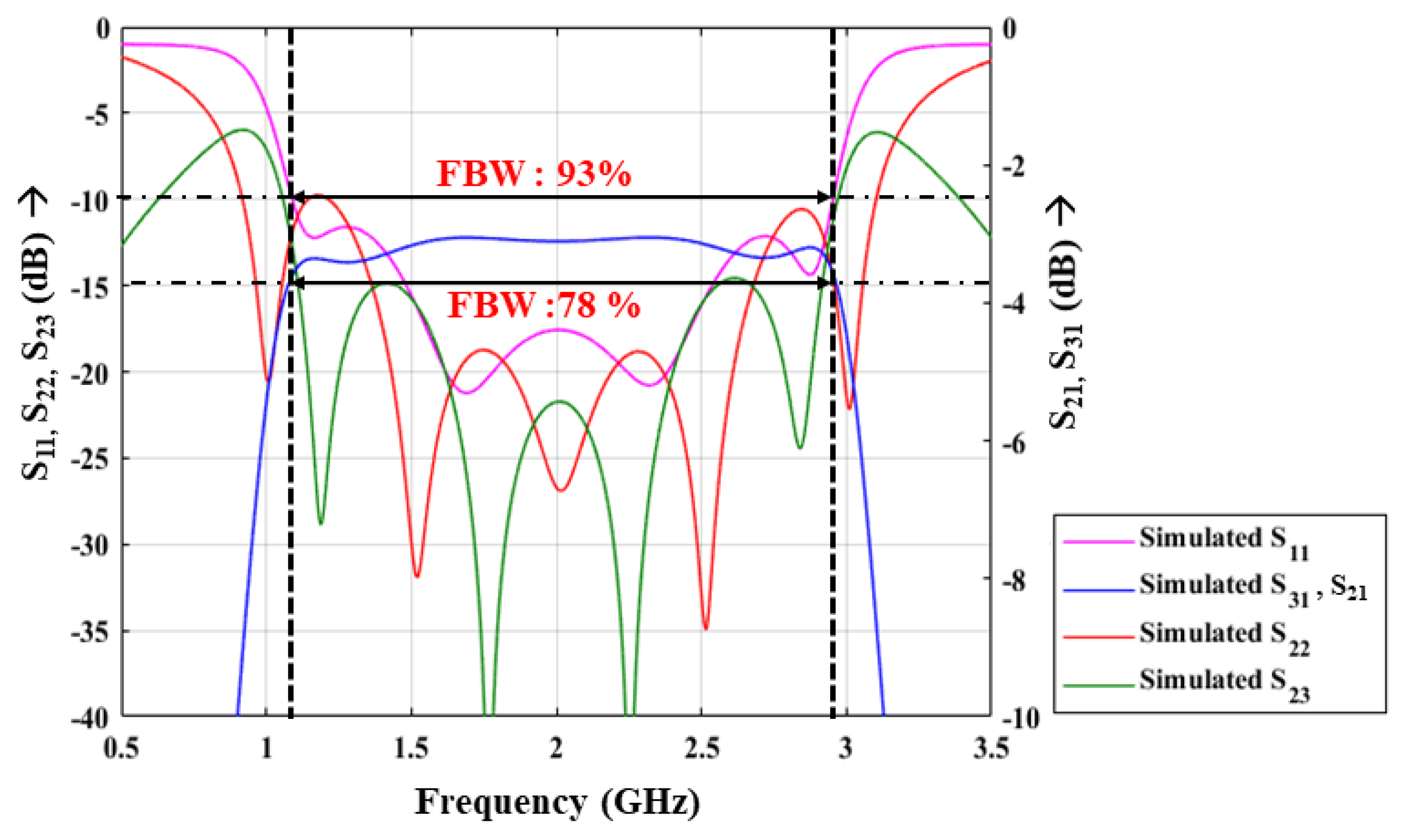
4. Wideband DC Isolated WPD

The schematic of the proposed wideband DC isolated WPD is shown in Figure 15. It comprises of core wideband WPD with coupled-lines having Z e , Z o as the even- and odd-mode characteristic impedance with electrical length θ = 90 at the input side for DC isolation. The Z S are port terminations at the input and output side.

4.1. Even-Mode Analysis

The even-mode half-network is presented in Figure 16. It is to be noted that the even-mode half-network is lossless and reciprocal, thus matching at port-1 and port-2 remains the same. As mentioned earlier, the port matching requirement at port 1 i.e., S 11 are related in terms of even-mode half-circuit port matching, S 11 e . This clearly conveys that Z i n should be equal to Z e q in Figure 16. For fulfilling the port matching requirement, the resulting equations are as follows (assuming that Z S 1 and Z S 2 result in open-circuit because of 90 electrical length):
Z x = Z B 2 Z S
Z e q = Z A 2 Z x = Z A 2 Z S Z B 2
The value of impedance looking into coupled line, Z i n can be calculated using Equation (16) [59], where Z x = ( Z e + Z o )/2 and Z y = ( Z e Z o )/2.
Z i n = j ( Z x cot θ ) + Z y 2 csc 2 θ Z S j Z x cot θ
For θ = 90 , (16) results in (17) and for matching conditions, Z i n = Z e q * which results in Equations (18a) and (18b).
Z i n = ( Z e Z o ) 2 4 Z S
Z e q = Z A 2 Z x = Z A 2 Z S Z B 2
( Z e Z o ) = 2 Z S Z A Z B
Equation (18b) is the design equation for the coupled line and it gives the difference between even and odd-mode characteristic impedance of the coupled line.

4.2. Odd-Mode Analysis

The odd-mode analysis of the DC isolated WPD is exactly the same as discussed in Section 2. Now, Table 2 provides the impedance parameters for wideband WPD with different θ c . The relation between R 1 and R 2 according to (14) is plotted in Figure 17 for different θ c . To better illustrate the isolation between two ports of WPD, considering the case-1 in Table 2, S 23 (dB) is plotted for different values of isolation resistors calculated from Figure 17. It can be observed from Figure 18 that the value of S 23 (dB) varies with different values of R 1 and R 2 . Figure 19, Figure 20 and Figure 21 presented the S p a r a m e t e r s (dB) for different cases with varying θ c and all parameters are within the realizable range of 20–160 Ω .
The approach described in Section 4 has been utilized to design a wideband DC isolated WPD with center frequency of 2 GHz and θ c = 55 . The prototype depicted in Figure 22 has been fabricated on RO4350B substrate with dielectric constant ( ϵ r = 3.66), dissipation factor = 0.0037 with substrate thickness of 1.52 mm. The prototype along with measurement setup is presented in Figure 23. The EM simulation and measured results are depicted in Figure 24 and Figure 25. It can be observed that there is a slight discrepancy in EM simulation and measurement results as a result of the utilization of bends and tapers post-processing to avoid junction discontinuities and substrate parameter variation. The measured return loss S 11 (dB) and isolation S 23 (dB) is better than −10 dB and −10 dB, respectively, within the frequency range of 1.0–3.0 GHz. The measured insertion losses at output ports, S 21 (dB) and S 31 (dB) are −3.0 ± 0.4 dB which is quite comparable to the simulated results of −3 dB. Table 3 presents the comparison of the proposed wideband WPD with the previous designed WPDs.

5. Conclusions

In this article, a two-section Wilkinson power divider exhibiting wideband performance with good port-to-port isolation is presented. It has been demonstrated that the two-section configuration, utilizing transmission lines and short-circuit stubs achieve wide pass-band and good in-band isolation. Closed-form design equations are presented along with a step-by-step design method for easy prototyping. Furthermore, a design expression for the isolation network is derived to determine the values of resistors. A variant is presented that utilizes coupled lines for DC isolation at the input side. A few case studies for both the designs have also been presented. An excellent agreement between theoretical, simulated and measured results validate the proposed synthesis procedure.

Author Contributions

Conceptualization, methodology, validation, investigation, writing, A.S.; writing–review and editing, D.B.; supervision, project administration, funding acquisition, M.H. and M.A.C. All authors have read and agreed to the published version of the manuscript.

Funding

This research was funded by Nazarbayev University with grant number: 021220CRP0222, 110119FD4515.

Data Availability Statement

Data is describing within the article. The data that support the findings of this study are available from the corresponding author upon reasonable request.

Acknowledgments

The writers would like to thank the editor and anonymous reviewers for their helpful comments for improving the quality of this paper.

Conflicts of Interest

The authors declare no conflict of interest.

References

  1. Gomez-Garcia, R.; Ghannouchi, F.M.; Carvalho, N.B.; Luong, H.C. Guest editorial advanced circuits and systems for CR/SDR applications. IEEE Trans. Emerg. Sel. Topics Circuits Syst. 2013, 3, 485–488. [Google Scholar] [CrossRef]
  2. Hallberg, W.; Ozen, M.; Kuylenstierna, D.; Buisman, K.; Fager, C. A generalized 3-db wilkinson power divider/combiner with complex terminations. IEEE Trans. Microw. Theory Tech. 2018, 66, 4497–4506. [Google Scholar] [CrossRef]
  3. Liu, Y. Synthesis techniques on multiband impedance matching networks for frequency-dependent complex loads. IEEE Trans. Microw. Theory Tech. 2018, 66, 4507–4519. [Google Scholar] [CrossRef]
  4. Maktoomi, M.A.; Hashmi, M.S.; Ghannouchi, F.M. A dual-band port-extended branch-line coupler and mitigation of the band-ratio and power division limitations. IEEE Trans. Comp. Packag. Manf. Tech. 2017, 7, 1313–1323. [Google Scholar] [CrossRef]
  5. Wilkinson, E.J. An N-way hybrid power divider. IRE Trans. Microw. Theory Tech. 1960, 8, 116–118. [Google Scholar] [CrossRef]
  6. Park, M.J.; Lee, B. A dual-band Wilkinson power divider. IEEE Microw. Wirel. Compon. Lett. 2008, 18, 85–87. [Google Scholar] [CrossRef]
  7. Wu, Y.; Liu, Y.; Zhang, Y.; Gao, J.; Zhou, H. A dual band unequal Wilkinson power divider without reactive components. IEEE Trans. Microw. Theory Tech. 2008, 57, 216–222. [Google Scholar]
  8. Zhang, H.L.; Hu, B.J.; Zhang, X.Y. Compact equal and unequal dual-frequency power dividers based on composite right-/left-handed transmission lines. IEEE Trans. Ind. Electron. 2012, 59, 3464–3472. [Google Scholar] [CrossRef]
  9. Al Shamaileh, K.; Dib, N.; Abushamleh, S. A dual-band 1:10 Wilkinson power divider based on multi-T-section characterization of high-impedance transmission lines. IEEE Microw. Wirel. Compon. Lett. 2017, 27, 897–899. [Google Scholar] [CrossRef]
  10. Wu, L.; Sun, Z.; Yilmaz, H.; Berroth, M. A dual-frequency Wilkinson power divider. IEEE Trans. Microw. Theory Tech. 2006, 54, 278–284. [Google Scholar] [CrossRef]
  11. Liu, F.X.; Lee, J.C. Design of new dual-band Wilkinson power dividers with simple structure and wide isolation. IEEE Trans. Microw. Theory Tech. 2019, 67, 3628–3635. [Google Scholar] [CrossRef]
  12. Pakasiri, C.; Wang, S. Dual-band compact wilkinson power divider using common inductor and complex load. IEEE Access 2020, 8, 97189–97195. [Google Scholar] [CrossRef]
  13. Gao, N.; Wu, G.; Tang, Q. Design of a novel compact dual-band Wilkinson power divider with wide frequency ratio. IEEE Microw. Wirel. Compon. Lett. 2014, 24, 81–83. [Google Scholar] [CrossRef]
  14. Okada, Y.; Kawai, T.; Enokihara, A. Design Method for Multiband WPDs Using Multisection LC-Ladder Circuits. IEEE Microw. Wirel. Compon. Lett. 2017, 27, 894–896. [Google Scholar] [CrossRef]
  15. Wang, X.; Ma, Z.; Ohira, M. Theory and experiment of two-section two-resistor Wilkinson power divider with two arbitrary frequency bands. IEEE Trans. Microw. Theory Tech. 2017, 66, 1291–1300. [Google Scholar] [CrossRef]
  16. Zhao, W.; Zhang, N.; Wu, B.; Wang, X.; Ma, Z.; Chen, C.P. A Dual-Band Wilkinson Power Divider Using Dual Coupled Lines and Open Stubs. In Proceedings of the IEEE MTT-S International Wireless Symposium (IWS), Shanghai, China, 20–23 September 2020; pp. 1–3. [Google Scholar]
  17. Maktoomi, M.H.; Banerjee, D.; Hashmi, M.S. An enhanced frequency-ratio coupled-line dual-frequency Wilkinson power divider. IEEE Trans. Circ. Sys. II 2017, 65, 888–892. [Google Scholar] [CrossRef]
  18. Song, A.; Wang, X.; Ma, Z.; Ohira, M. Design theory of dual-band Wilkinson power divider with different frequency ratio ranges. In Proceedings of the IEEE Asia-Pacific Microwave Conference (APMC), Kyoto, Japan, 6–9 November 2018; pp. 1489–1491. [Google Scholar]
  19. Chu, Q.X.; Lin, F.; Lin, Z.; Gong, Z. Novel design method of tri-band power divider. IEEE Trans. Microw. Theory Tech. 2011, 59, 2221–2226. [Google Scholar] [CrossRef]
  20. Abdelrahman, B.M.; Ahmed, H.N.; Nashed, A.I. A novel tri-band Wilkinson power divider for multiband wireless applications. IEEE Microw. Wirel. Compon. Lett. 2017, 27, 891–893. [Google Scholar] [CrossRef]
  21. Chen, H.H.; Pang, Y.H. A tri-band Wilkinson power divider utilizing coupled lines. In Proceedings of the 2011 IEEE International Symposium on Antennas and Propagation (APSURSI), Spokane, WA, USA, 3–8 July 2011; pp. 25–28. [Google Scholar]
  22. Papanastasiou, A.C.; Georghiou, G.E.; Eleftheriades, G.V. A quad-band Wilkinson power divider using generalized NRI transmission lines. IEEE Microw. Wirel. Compon. Lett. 2008, 18, 521–523. [Google Scholar] [CrossRef]
  23. Singh, P.K.; Basu, S.; Wang, Y.H. Coupled line power divider with compact size and bandpass response. Electron. Lett. 2009, 45, 892–894. [Google Scholar] [CrossRef]
  24. Li, Y.C.; Xue, Q.; Zhang, X.Y. Single-and dual-band power dividers integrated with bandpass filters. IEEE Trans. Microw. Theory Tech. 2013, 61, 69–76. [Google Scholar] [CrossRef]
  25. Gao, S.S.; Sun, S.; Xiao, S. A novel wideband bandpass power divider with harmonic-suppressed ring resonator. IEEE Microw. Wirel. Compon. Lett. 2013, 23, 119–121. [Google Scholar] [CrossRef] [Green Version]
  26. Song, K.; Ren, X.; Chen, F.; Fan, Y. Compact in-phase power divider integrated filtering response using spiral resonator. IET Microw. Ant. Prop. 2014, 8, 228–234. [Google Scholar] [CrossRef]
  27. Shao, J.Y.; Huang, S.C.; Pang, Y.H. Wilkinson power divider incorporating quasi-elliptic filters for improved out-of-band rejection. Electron. Lett. 2011, 47, 1288–1289. [Google Scholar] [CrossRef]
  28. Li, Q.; Zhang, Y.; Wu, C.T.M. High-selectivity and miniaturized filtering Wilkinson power dividers integrated with multimode resonators. IEEE Trans. Compon. Packag. Manuf. Technol. 2017, 7, 1990–1997. [Google Scholar] [CrossRef]
  29. Zhang, X.Y.; Wang, K.X.; Hu, B.J. Compact filtering power divider with enhanced second-harmonic suppression. IEEE Microw. Wirel. Compon. Lett. 2013, 23, 483–485. [Google Scholar] [CrossRef]
  30. Liu, Y.; Sun, S.; Yu, X.; Wu, Y.; Liu, Y. Design of a wideband filtering power divider with good in-band and out-of-band isolations. Int. J. RF Microw. Comp.-Aided Eng. 2019, 29, e21728. [Google Scholar] [CrossRef]
  31. Wang, X.; Wang, J.; Zhang, G.; Hong, J.S.; Wu, W. Dual-wideband filtering power divider with good isolation and high selectivity. IEEE Microw. Wirel. Compon. Lett. 2017, 27, 1071–1073. [Google Scholar] [CrossRef]
  32. Song, K.; Xue, Q. Novel ultra-wideband (UWB) multilayer slotline power divider with bandpass response. IEEE Microw. Wirel. Compon. Lett. 2009, 20, 13–15. [Google Scholar] [CrossRef]
  33. Ren, X.; Xu, K.D. Multilayer balanced-to-unbalanced power divider with wideband transmission characteristic and common-mode suppression. IEEE Trans. Comp. Packag. Manf. Tech. 2018, 9, 72–79. [Google Scholar] [CrossRef]
  34. Zhu, H.; Cheng, Z.; Guo, Y.J. Design of wideband in-phase and out-of-phase power dividers using microstrip-to-slotline transitions and slotline resonators. IEEE Trans. Microw. Theory Tech. 2019, 67, 1412–1424. [Google Scholar] [CrossRef]
  35. Guo, L.; Abbosh, A.; Zhu, H. Ultra-wideband in-phase power divider using stepped-impedance three-line coupled structure and microstrip-to-slotline transitions. Electron. Lett. 2014, 50, 383–384. [Google Scholar] [CrossRef]
  36. Chen, J.-X.; Chin, C.H.K.; Lau, K.W.; Xue, Q. 180° out-of-phase power divider based on double-sided parallel striplines. Electron. Lett. 2006, 42, 1229–1230. [Google Scholar] [CrossRef]
  37. Bialkowski, M.E.; Abbosh, A.M. Design of a compact UWB outof-phase power divider. IEEE Microw. Wirel. Compon. Lett. 2007, 17, 289–291. [Google Scholar] [CrossRef]
  38. Ahmed, U.T.; Abbosh, A.M. Wideband out-of-phase power divider using tightly coupled lines and microstrip to slotline transitions. Electron. Lett. 2016, 52, 126–128. [Google Scholar] [CrossRef]
  39. Liu, Y.; Zhu, L.; Sun, S. Proposal and Design of a Power Divider With Wideband Power Division and Port-to-Port Isolation: A New Topology. IEEE Trans. Microw. Theory Tech. 2020, 68, 1431–1438. [Google Scholar] [CrossRef]
  40. Chen, D.; Zhu, L.; Cheng, C. Dual-resonant-mode (DRM) impedance transformer and its application to wideband 3 dB power divider. IEEE Microw. Wirel. Compon. Lett. 2013, 23, 471–473. [Google Scholar] [CrossRef]
  41. Weng, M.; Song, Y.; Zhao, J. Design of compact microstrip UWB power divider using square ring multiple-mode resonator. Asia-Pac. Microw. Conf. (APMC) 2015, 1, 1–3. [Google Scholar]
  42. Zhu, H.; Abbosh, A.M.; Guo, L. Wideband four-way filtering power divider with sharp selectivity and wide stopband using looped coupled line structures. IEEE Microw. Wirel. Let. 2016, 26, 413–415. [Google Scholar] [CrossRef]
  43. Jiao, L.; Wu, Y.; Liu, Y.; Xue, Q.; Ghassemlooy, Z. Wideband filtering power divider with embedded transversal signal-interference sections. IEEE Microw. Wirel. Compon. Lett. 2017, 27, 1068–1070. [Google Scholar] [CrossRef]
  44. Song, K.; Mo, Y.; Fan, Y. Wideband four-way filtering-response power divider with improved output isolation based on coupled lines. IEEE Microw. Wirel. Compon. Lett. 2014, 24, 674–676. [Google Scholar] [CrossRef]
  45. Tang, C.W.; Chen, J.T. A design of 3-dB wideband microstrip power divider with an ultra-wide isolated frequency band. IEEE Trans. Microw. Theory Tech. 2016, 64, 1806–1811. [Google Scholar] [CrossRef]
  46. Li, L.; Li, Z.F. Side-coupled shorted microstrip line for compact quasi-elliptic wideband bandpass filter design. IEEE Microw. Wirel. Compon. Lett. 2010, 20, 322–324. [Google Scholar] [CrossRef]
  47. Xu, K.D.; Bai, Y.; Ren, X.; Xue, Q. Broadband filtering power dividers using simple three-line coupled structures. IEEE Trans. Compon. Packg. Manf. Technol. 2018, 9, 1103–1110. [Google Scholar] [CrossRef]
  48. Dang, T.S.; Kim, C.W.; Yoon, S.W. Ultra-wideband power divider using three parallel-coupled lines and one shunt stub. Electron. Lett. 2014, 50, 95–96. [Google Scholar] [CrossRef]
  49. Guo, L.; Zhu, H.; Abbosh, A.M. Wideband tunable in-phase power divider using three-line coupled structure. IEEE Microw. Wirel. Compon. Lett. 2016, 26, 404–406. [Google Scholar] [CrossRef]
  50. Yu, X.; Sun, S. A novel wideband filtering power divider with embedding three-line coupled structures. IEEE Access 2018, 6, 41280–41290. [Google Scholar] [CrossRef]
  51. Oraizi, H.; Sharifi, A.-R. Optimum design of asymmetrical multisection two-way power dividers with arbitrary power division and impedance matching. IEEE Trans. Microw. Theory Tech. 2011, 59, 1478–1490. [Google Scholar] [CrossRef]
  52. Wong, S.W.; Zhu, L. Ultra-wideband power divider with good in-band splitting and isolation performances. IEEE Microw. Wirel. Compon. Lett. 2008, 18, 518–520. [Google Scholar] [CrossRef]
  53. Xu, Y.; Bosisio, R. Design of multiway power divider by using stepped-impedance transformers. IEEE Trans. Microw. Theory Tech. 2012, 60, 2781–2790. [Google Scholar] [CrossRef]
  54. Maktoomi, M.A.; Hashmi, M.S.; Ghannouchi, F.M. Theory and design of a novel wideband DC isolated Wilkinson power divider. IEEE Microw. Wirel. Compon. Lett. 2016, 26, 586–588. [Google Scholar] [CrossRef]
  55. Kao, J.-C.; Tsai, Z.M.; Lin, K.-Y.; Wang, H. A modified Wilkinson power divider with isolation bandwidth improvement. IEEE Trans. Microw. Theory Tech. 2012, 60, 2768–2780. [Google Scholar] [CrossRef]
  56. Tas, V.; Atalar, A. An optimized isolation network for the Wilkinson divider. IEEE Trans. Microw. Theory Tech. 2014, 62, 3393–3402. [Google Scholar] [CrossRef] [Green Version]
  57. Yu, T.; Tsai, J.-H.; Chang, Y. A radial four-way power divider with the proposed isolation network. IEEE Microw. Wirel. Compon. Lett. 2018, 28, 194–196. [Google Scholar] [CrossRef]
  58. Wang, X.; Sakagami, I.; Mase, A.; Ichimura, M. Wilkinson power divider with complex isolation component and its miniaturization. IEEE Trans. Microw. Theory Tech. 2014, 62, 422–430. [Google Scholar] [CrossRef]
  59. Pozar, D.M. Microwave Engineering; John Wiley and Sons: Hoboken, NJ, USA, 2009. [Google Scholar]
  60. Riblet, H.J. General synthesis of quarter-wave impedance transformers. IRE Trans. Microw. Theory Tech. 1957, 5, 36–43. [Google Scholar] [CrossRef]
Figure 1. Schematic of the proposed wideband WPD.
Electronics 10 02168 g001
Figure 2. Even-Mode Half-Circuit.
Electronics 10 02168 g002
Figure 3. Transfer characteristics of the proposed network.
Electronics 10 02168 g003
Figure 4. Transfer characteristics of Chebyshev Bandpass Filter.
Electronics 10 02168 g004
Figure 5. Odd-Mode Half-Circuit.
Electronics 10 02168 g005
Figure 6. Transformed Odd-Mode Half-Circuit.
Electronics 10 02168 g006
Figure 7. Relation between isolation resistor values.
Electronics 10 02168 g007
Figure 8. Simulated S-parameters Response for θ c = 55 .
Electronics 10 02168 g008
Figure 9. Simulated S-parameters for θ c = 60 .
Electronics 10 02168 g009
Figure 10. Simulated S-parameters for θ c = 65 .
Electronics 10 02168 g010
Figure 11. Fabricated prototype of the proposed WPD.
Electronics 10 02168 g011
Figure 12. Measurement Setup for (A): S 11 ; (B): S 21 for θ c = 55 .
Electronics 10 02168 g012
Figure 13. EM vs. Measured S-parameters for (A) S 11 ; (B) S 23 , S 22 for θ c = 55 .
Electronics 10 02168 g013
Figure 14. EM vs. Measured S-parameters for (A) S 21 ; (B) S 31 for θ c = 55 .
Electronics 10 02168 g014
Figure 15. Schematic of the proposed DC Isolated wideband WPD.
Electronics 10 02168 g015
Figure 16. Even-mode analysis of half-network.
Electronics 10 02168 g016
Figure 17. Relation between R 1 and R 2 for different θ c .
Electronics 10 02168 g017
Figure 18. Variation of S 23 (dB) for θ c = 55 with different isolation resistors.
Electronics 10 02168 g018
Figure 19. Simulated S p a r a m e t e r s (dB) for θ c = 55 .
Electronics 10 02168 g019
Figure 20. Simulated S p a r a m e t e r s (dB) for θ c = 60 .
Electronics 10 02168 g020
Figure 21. Simulated S p a r a m e t e r s (dB) for θ c = 65 .
Electronics 10 02168 g021
Figure 22. Fabricated prototype of the proposed DC isolated WPD.
Electronics 10 02168 g022
Figure 23. Measurement Setup for (A): S 23 ; (B): S 21 for θ c = 55 .
Electronics 10 02168 g023
Figure 24. EM vs. Measured S-parameters for (A) S 21 ; (B) S 31 for θ c = 55 .
Electronics 10 02168 g024
Figure 25. EM vs. Measured S-parameters for (A) S 11 ; (B) S 23 , S 22 for θ c = 55 .
Electronics 10 02168 g025
Table 1. Design Parameters of Wideband WPD.
ParametersCases
θ c 55 60 65
Z A ( Ω )115127120
Z B ( Ω )819094
Z S 1 ( Ω )1105535
Z S 2 ( Ω )403124
R 1 ( Ω )13194162
R 2 ( Ω )200150200
Table 2. Design Parameters of DC Isolated WB WPD.
ParametersCases
θ c 55 60 65
Z A ( Ω )11050.8235
Z B ( Ω )88.6312792
Z S 1 ( Ω )56.59068
Z S 2 ( Ω )7047.448
Z e ( Ω )131160129
Z o ( Ω )306942
R 1 ( Ω )3810062
R 2 ( Ω )150150150
Table 3. Comparison with previous wideband WPDs.
ReferenceFrequency Range
(GHz)
TopologyFBW *
(| S 21 = S 31 |)
DC
Isolation
Isolation
Network
Size
( λ g × λ g )
MWCL
[40]
2.7–4.7Dual Resonant Modes
in single resonator
53.5%
(3 dB)
No1 Resistor1.06 × 0.89
MWCL
[54]
1.25–2.5Coupled-lines
at Input/Output port
51%
(3 dB)
Yes1 Resistor0.89 × 0.57
TMTT
[45]
1.45–4.6Quasi-coupled
Lines
77%
(3 dB)
No1 Resistor
1 Capacitor
0.2 × 0.15
MWCL
[43]
1.55–4.24Embedded Transversal
Signal Interference
84%
(3 dB)
No1 Resistor
1 Inductor
1 Capacitor
0.8 × 0.5
Access
[50]
1.42–3.42Three Line coupled
structure
58%
(3 dB)
Yes1 Resistor0.62 × 0.5
TCPMT
[47]
1.5–3.55Three Line Coupled
structure
64%
(3 dB)
No1 Resistor0.05 × 0.32
This Work1.3–2.9Two-stage
Configuration
80%
(3 dB)
No2 Resistors1.03 × 0.62
1.01–3.02Two-stage
with Coupled Lines
82.5%
(3 dB)
Yes2 Resistors1.2 × 0.86
* FBW—Fractional Bandwidth.
Publisher’s Note: MDPI stays neutral with regard to jurisdictional claims in published maps and institutional affiliations.

