1. Introduction
The reconfigurable metasurface (MS) field has grown dramatically in recent years, with many MS studies in various frequencies and methods for different applications [
1,
2,
3,
4,
5]. MS is a private case of a metamaterial in which a surface configuration containing a two-dimensional (2-D) array of cyclic or semi-cyclic unit cells smaller than the operating wavelength. This spatial arrangement gives the material properties at the macroscopic level that do not exist directly in its natural structure. Like ordinary homogeneous materials composed of atoms at the microscopic level, the “new” material comprises individual unit cells, which are meta-atoms at the microscopic level [
6,
7]. Since the periodic meta-atomic structure functions as “atoms” in a homogeneous material, the wavelength of the relevant radiation must be greater than the “meta-atomic” dimensions. The larger the wavelength relative to the meta-atom, the higher the uniformity of the homogeneous material property at the macroscopic level. MS is used in nanotechnology, radar, antennas, optical lenses, and more [
1,
2,
3,
4,
5]. Adding a tunable element to the MS unit cells enables a wide range of applications, such as a reconfigurable beam-steering reflector [
8], reflective surface that functions as a parabolic mirror with an adjustable focus [
9], and more [
1,
2,
3,
4,
5]. The common MS unit cell type is the resonant unit cell [
8]. Around the unit cell resonance frequency
fres, the unit cell reflection phase values change significantly. Thus, changing the
fres around the operating frequency enables a high dynamic phase range at the operating frequency. The ability to continuously control and reconfigure the reflection phase value’s distribution throughout the MS reflector allows for creating an appropriate reflection phase petrean on the MS. This enables reflected beam steering. This approach is called phase-gradient MS [
10]. However, a major barrier to adopting MS solutions is the relatively high losses that are associated with the resonant characteristic of the unit cell. There are two mains loss mechanisms in the MS applications based on continuous control over the reflection phase values of the unit cell:
- (1)
Phase errors resulting from the dynamic reflection phase range of less than 360°.
- (2)
The unit cell resistance R causes losses, mainly at phase values around the fres.
The chosen method for tuning capability parameter is defined as
TC and the parameter of the unit cell
Q-factor as
Q. The unit cell dynamic reflection phase range is proportional to
TC ×
Q; therefore, a small
TC can be compensated by increasing the
Q. It also increases unit cell losses proportional to
R ×
Q [
11]. On the other hand, a large
TC allows for a reduction in
Q and unit cell losses while maintaining a high dynamic phase reflection range. Several methods add reconfiguring and tuning to MS, such as PIN switches, MEMS switches, liquid crystal materials, piezoelectric materials, and varactor diodes [
8,
9,
12,
13,
14,
15,
16,
17,
18,
19,
20,
21,
22]. The liquid crystal method is used in the K-band and above and can be realized in MS as a tuning dielectric substrate, without any external element in the front, but is more challenging to implement [
16]. The dielectric constant is the fundamental parameter, which changes in the liquid crystal tuning method. This parameter varies slightly in the order of tens of percent with a relatively low
TC. Thus, increasing the
Q of the unit cell compensates for the inherent low tunability and allows for a significant dynamic phase range, but increasing
Q also increases the losses, frequency dispersion, sensitivity to tolerances, and decreases bandwidth [
16]. The liquid crystal has a slow response time, which is slower than the diode varactors’ and switches’ response times by several orders of magnitude [
23]. Thus, liquid crystal is less suitable for continuous tracking and switching applications. Piezoelectric microelectromechanical system (MEMS) materials enable continuous changes in the unit cell thickness depending on the DC voltage [
12,
22]. Thus, the properties of the MS continuously change as well. Using the piezo MEMS method is limited because it involves a physical change in the unit cell size. In addition, a high voltage of up to 200 V is needed for the control [
22]. Several methods of tuning for digital coding MS applications are with quantization control over the unit cell reflection phase, mainly switches. The PIN switch enables frequency work up to 70 GHz, with a fast switching time, high reliability, low cost, and low control voltage of switches for digital coding MS applications with quantization control over the unit cell reflection phase [
24,
25]. Recently, the MEMS switch aroused attention due to its small size and linearity [
26,
27], but it has a relatively slow switching time compared to the PIN switch [
24]. In addition, many switch components operate at voltage levels of 0 V and 5 V, which are standard voltages for controllers and electronic components that simplify the realization of the DC biasing circuit. However, the discrete nature of the switch state prevents the switches from being used in applications where a continuous phase change is required. The switches do not meet our basic requirement since it is impossible to achieve high-resolution beam steering, let alone the possibility of continuous tracking for surfaces that are not unusually large.
A varactor diode allows for a continuous and high-tuning-capacitance ratio and fits the continuous reflection phase method in the proposed MS reflector [
8,
14,
15,
17,
18,
19,
28,
29,
30]. The varactor diodes allow for high-frequency work up to 70 GHz, a conventional PCB assembly, and extremely low consuming power [
31], and thus leads to a focus on the varactor diode in this study. However, the varactor diode suffers from relatively high losses compared to the switches. The losses effect is reduced by decreasing
Q [
11,
17,
18,
19]. The reduction in
Q is justified due to the very high tunability of the varactor diode capacitance value with a high
TC parameter. In addition, using the quantization reflection phase method compared to the continuous reflection phase method adds quantization losses for beam steering of about 4 dB for 1-bit digital coding MS and about 1 dB for 2-bit digital coding MS [
32,
33]. Thus, considering the total losses budget for a beam-steering application, using the varactor diode seems better, but additional research is required. Therefore, considering the total losses budget for a beam-steering application, using the varactor diode seems better, but further research is required.
A reconfigurable MS reflector based on varactor diodes as a tuning element is well known with many published implementations operating at frequencies of up to 6 GHz [
8,
15,
28,
29], with very few at X-band and above [
18,
30,
34], where one of them [
34] is categorized as a sparse MS and not as a classic MS. Such implementations in the X-band and above will improve satellite communications’ quality of service (QoS) in the X-band and Ku-band [
35]. Furthermore, an MS reflector with a high range and accurate beam steering enables the coverage of shaded areas and improved quality of service, including beam tracking. Such continuously reconfigurable MS reflectors for high-resolution beam steering operating above the X-band frequency are needed to improve satellite communication.
However, the implementation of reconfigurable MS above the X-band, based on a varactor diode as a tuning element, is challenging due to the constraint to reduce unit cell dimensions and increasing the diodes’ density on the surface while maintaining the performance. In addition, the varactors require many DACs, complicating the realization of the DC biasing circuits in small dimensions.
2. Continuous Beam Steering MS Reflector Concept
The schematic structure of the designed MS reflector and its equivalent electric circuit model are shown in
Figure 1.
Figure 1a shows the basic MS reflector structure composed of a printed metal shape on a dielectric substrate. The printed metal shape on the front side can be a patch, a slot, a ring [
1,
36], or more complex geometries, such as a K-shape [
14], connected via a metal surface used as a ground plane at the backside.
Figure 1b presents the equivalent circuit of lumped elements with inductance, capacitance, and resistance components for the destined unit cell [
11].
The plane wave electric field component interacts with the patches’ edges, arousing surface charges (marked by +/− signs in
Figure 1a); this is modeled as a capacitance
C. The magnetic flux developing from the current (marked by dashed arrows in
Figure 1a) between the patch and the ground plane through the via is modeled as an inductance
L. The dielectric and ohmic losses are modeled as a resistance
R, which is the dissipation resistive part of the unit cell. When the unit cells are arranged in a 2-D periodic configuration, the surface is characterized as an effective impedance surface, which was defined by Dan Sievenpiper’s work [
11] with the surface impedance parameter
ZS, which is shown in Equation (1):
where around the angular frequency values of
, the imaginary part of the
ZS becomes dominant, and is shown in Equation (2):
The values of
C and
L are determined by the unit cell’s dimensions, geometry, materials, and PCB properties. The parallel resonance frequency
fres of the circuit model around which the radiation is manipulated is shown in Equation (3):
The bandwidth of the resonance frequency [
37] is shown in Equation (4):
The Q-factor is shown in Equation (5):
According to the phased array theory, each unit cell location on the MS is defined at its center [
38]. A 2-D surface in the
XY plane with a spatial array arrangement of a fixed distance and a 90° angle between the unit cells is defined as S (
xj,
yi),
j = 1, 2, …,
N and
i = 1, 2, …,
M, where
N and
M are integer numbers that lead to an array of
N ×
M unit cells. This unit cell array with the desired phase distribution throughout the surface allows for focusing radiation to the desired point [
9] or radiation steering to the desired direction [
8]. A scheme of a beam-steering side cross-section view that is representative of an MS reflector is shown in
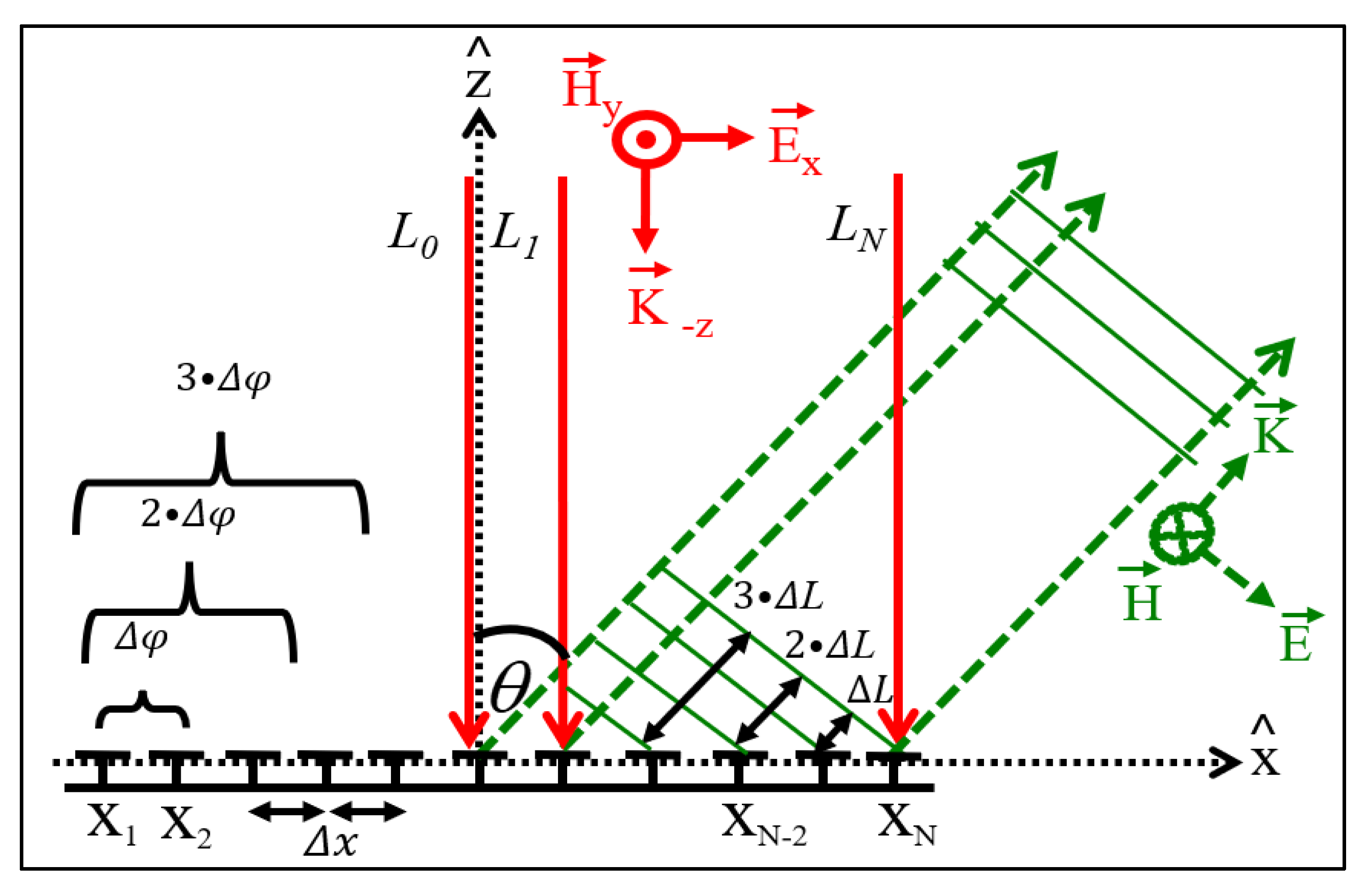
Figure 2.
Figure 2 shows a scheme of radiation steering using an MS reflector, where
L1,
L2, and
LN are incident rays toward the surface marked in red arrows. The optical path difference (OPD) between the reflected rays from unit cells
Xj to
Xj+1 is defined as
ΔL and is described in Equation (6):
where
ΔX is the array constant. For beam steering,
ΔL is constant for all different paths from adjacent cells
Xj and
Xj+1 throughout the surface. The conversion of
ΔL into a phase difference is shown in Equation (7):
where
λ is the wavelength at the working frequency. By supplying the accumulated phase difference
Δφx from left to right throughout the surface, between adjacent unit cells
Xj and
Xj+1 in the x-axis, each reflected ray marked in dashed green arrows gets additional accumulated
ΔL. Thus, it leads to the desired steering angle
θ in the
XZ plane, as shown in
Figure 2. Using Equations (6) and (7), the connection between
Δφ and
ΔX to the desired angle steering
θ is shown in Equation (8):
The 2-D periodic structures can be simulated in three-dimensional electromagnetic simulation software, such as HFSS and CST [
39]. Due to their importance, there are dedicated simulation solvers that simplify the process and save time. In addition, these solvers enable extracting the surface reflection properties and dispersion diagram from a single unit cell simulation [
40].
To illustrate the resolution limit of digital coding metasurface, using the conceptual surface of 16 columns composed of 5 mm unit cells, with 2-bit coding, at an operating frequency of 10 GHz, and a planned beam-steering to
θ = 1° in
XZ plane, as defined in
Figure 2, is demonstrated. The four-phase state’s phase range definition, the desired reflection phase-gradient, and the distribution of the final state are shown in
Figure 3.
Figure 3 shows the phase value required for the desired beam steering for each unit cell. According to Equation (8),
Δϕ = 1.05°, and the cumulative phase difference is 1.05 × 15 = 15°, which is less than 90°. Since all phase values are between 0 and 90°, the entire unit cell surface is set to state ‘1,’ and there is no manipulation of the beam reflection direction. For beam steering of
θ = 5°, where
Δϕ = 5.23° and the cumulative phase difference is 5.23° × 15 = 78.45°, there is still no change in the unit cell state. Adding a constant phase to the entire MS that does not affect the phase gradient [
13] leads to a maximum of two-phase states for use, as shown in
Figure 4.
As shown in
Figure 4, the eight unit cells on the left are defined as phase state ‘1,’ and the eight unit cells on the right are defined as phase state ‘2.’ A change in the constant phase value leads to a change in the unit cells states for the same planed phase gradient; therefore, there is no single-valued par unit cell state for a given phase gradient. This inherent resolution difficulty of the digital coding of an MS reflector can be solved using unit cells, which provide a continuous reflection phase. The phase gradient is applied directly to the unit cells, as shown in
Figure 4, line 2.
3. Unit Cell and MS Reflector Concept and Design
The unit cell design was adopted and optimized for the X-band and Ku-band using mushroom geometry combined with a varactor diode. Such an MS structure is also known as a reconfigurable high impedance surface due to its reflection properties compared to a metal surface [
36]. The geometry and dimensions of the optimized unit cell and the standard unit cell are shown in
Figure 5.
Figure 5a,b shows the unit cell structure, with the varactor diode marked in a green rectangle. The unit cell area sizes are 4.2 mm × 4.2 mm, with a thickness of 1.68 mm. The unit cell sizes in wavelength units are 0.168
λ0 × 0.168
λ0 × 0.065
λ0, where
λ0 is the free-space wavelength at the operation frequency of 12 GHz. The main unit cell dimension parameters are shown in
Figure 5a. The unit cell comprises two dielectric substrates of the Rogers company, model 5880LZ, with a thickness of 0.762 mm and a dielectric constant
εr = 2 [
41], and three copper layers (in yellow), each with a thickness of 0.0175 mm. The top copper layer is the square patch. The middle copper layer is for metal ground purposes, separated by a clearance from the via that crosses it. The back-side copper layer is for DC biasing purposes, which is connected by a via with a diameter of 0.3 mm to the top copper layer, thus, to the varactor (shown in
Figure 5b).
The unit cell geometry, dimensions, materials, varactor, and the PCB manufacturing process quality determine the total capacitance
C and the inductance
L. The surface area and the patch size of the unit cell are proportional to the unit cell’s intrinsic capacitance
Cint. The thickness of the dielectric substrate is proportional to the unit cell’s intrinsic inductance
Lint [
8,
11].
Adding the variable varactor capacitance
Cd to the MS changes the total unit cell capacitance
C to
C =
Cint +
Cd. The total unit cell inductance is defined as
L =
Lint for the equivalent circuit model in
Figure 1b and Equations (1)–(5).
Reducing the unit cell’s dimensions decreases the
LC product in Equation (3), which is necessary for high
fres values. As shown in Equation (5), reducing
C decreases the
Q and thus the total unit cell losses
R × Q. Therefore, reducing
Cint values rather than
L is required to decrease the
LC product in Equation (3), allowing for a high operation frequency. Furthermore, the decrease in
C values increases the bandwidth and minimizes the phase errors (see Equation (4)). The unit cell’s low capacitance and the high tuning capacitance ratio are the fundamental requirements for allowing high-frequency implementation of the reconfigurable phase gradient MS reflector with continuous reflection phase control. Following these requirements, a varactor diode of MACOM model MAVR–011020-11411 was chosen as a tuning element. It allows for a continuous and high dynamic range regarding the capacitance value. To the best of our knowledge, this varactor diode has the lowest capacitance in the market. The varactors enable high-frequency operation; a continuous, high-capacitance dynamic range; low power consumption; and simplicity in manufacturing [
42]. Decreasing the value of
Cint makes the value of
Cd more dominant in the total unit cell capacitance
C and increasing its dynamic tuning range. Using a dielectric substrate with
εr = 2 and reducing the unit cell and patch sizes reduces the value of
Cint [
11,
17,
18,
19,
36]. The reduction in the patches prevented the varactor from being placed directly on the adjacent patches’ edges (blind pad), as in other works [
8,
15,
28,
30]. In this design, the distance between the unit cell patches edges was 1.34 mm, while the varactor length dimension is 0.76 mm [
42]. This point is demonstrated in
Figure 5c. For standard mushroom unit cell configuration, reducing the distance between the patch’s edges compared to the varactor length dimension allows the varactor assembly directly on the patches’ edges. But, it increased the
Cint, which impaired the ability and quality of the realization for the X-band frequencies and above. Thus, the varactor diodes were placed between the unit cells’ patches on the customized pads according to the layout of the varactor, which required the proper design of vertical lines from the patches to the customized pads, as shown in
Figure 5b. To overcome this limitation, the varactor diodes were placed between the unit cells’ patches on the customized pads according to the varactor layout, which required the proper design of vertical lines from the patches to the pads, as shown in
Figure 5b.
The maximum and minimum values of the diode capacitance for three voltage states (0, 4, and 15 volts) are given in the datasheet without providing a typical value. As a result, there is a non-uniformity in the simulation-defined
Cmax and
Cmin capacitance values in published works that use this diode. For example, in [
43],
Cmax = 0.27 pF and
Cmin = 0.032 pF; in [
44],
Cmax = 0.19 pF and
Cmin = 0.025 pF; and in [
45],
Cmax = 0.25 pF and
Cmin = 0.033 pF. These varactor capacitance values are critical for design considerations. Therefore, for reducing uncertainty in the varactor capacitance values, the average capacitances values of
Cmax and
Cmin are 0.21639 pF and 0.03258 pF, respectively, and were provided after contacting MACOM. A good agreement was obtained in our previous work between the measurements and the simulations based on the provided average capacitance values [
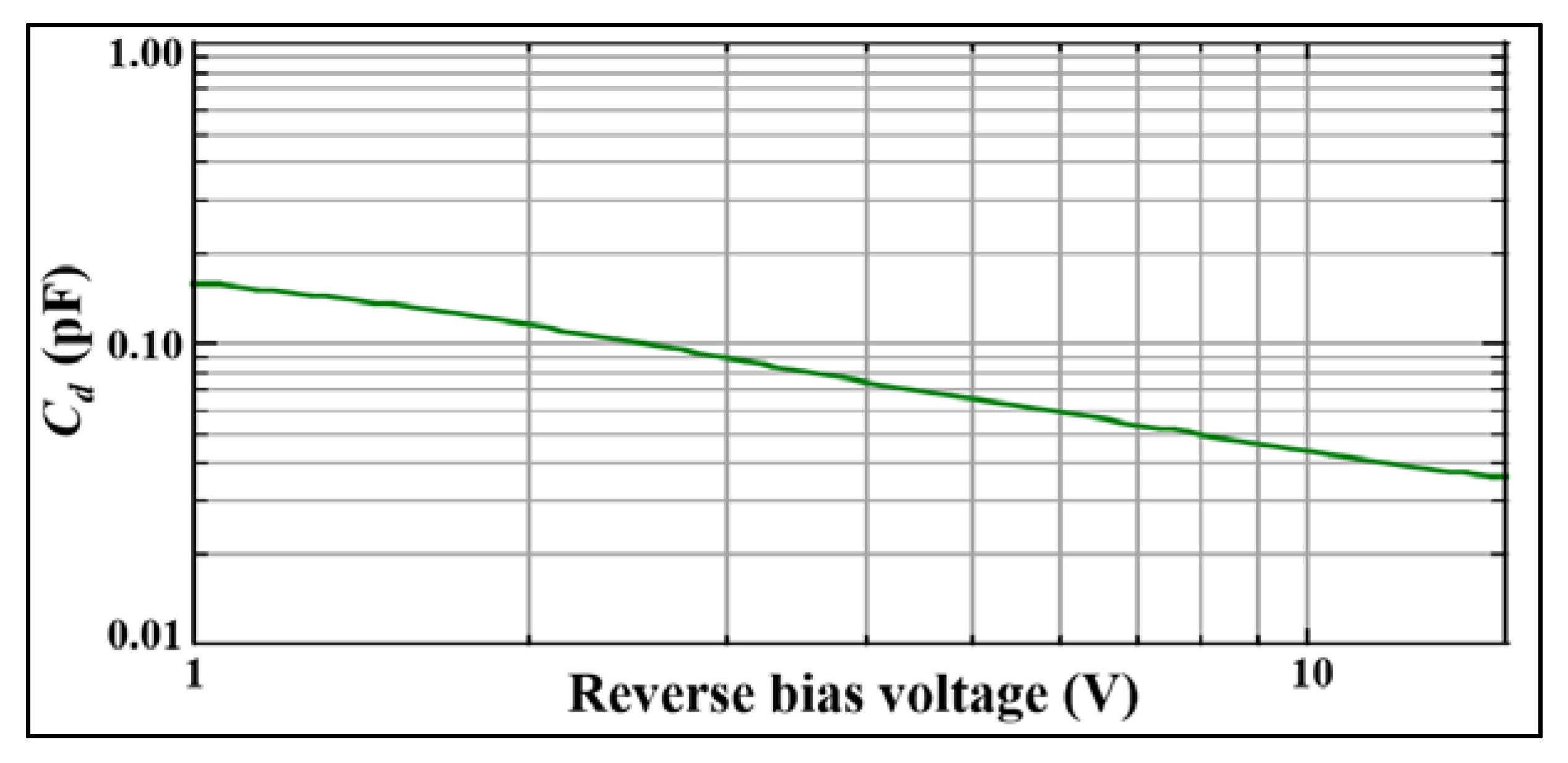
18]. The varactor edges’ capacitance values’ tolerance was considered in the unit cell’s design stage, which minimized its effect. In addition, the varactor has a constant gamma around one, which allows for linear tuning within the reverse bias voltage range of 2 to 12 V [
42], as shown in
Figure 6.
A prototype based on this unit cell was manufactured. This prototype allowed one-dimensional reflection phase control, where each column was separately stimulated with a DC bias. A photo of the prototype is shown in
Figure 7.
Figure 7 shows the manufactured 40-row and 33-column MS, summing up to 1320 unit cells. The MS area sizes were 185 mm × 140.6 mm (7.4
λ0 × 6.2
λ0 in wavelength units at 12 GHz).
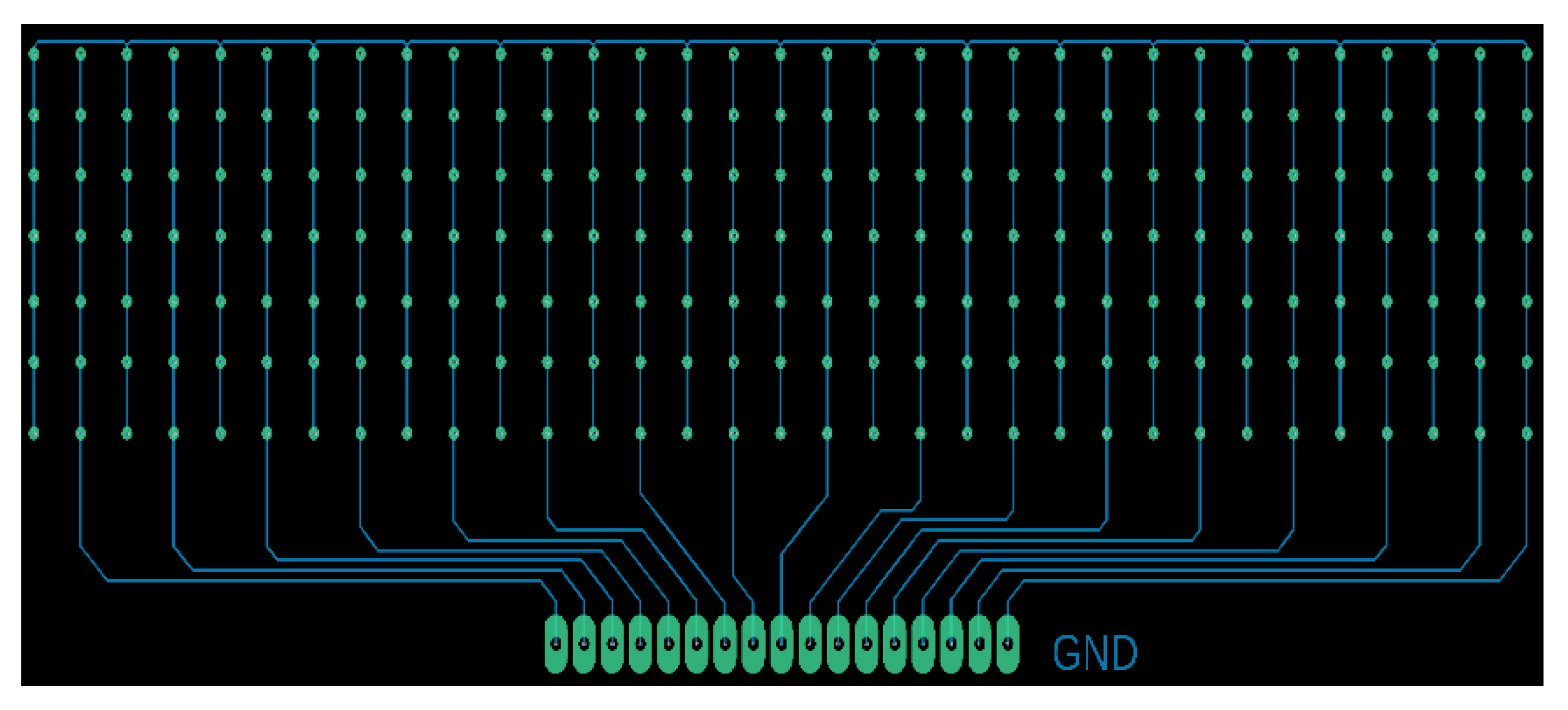
The design of the MS prototype bottom layer, which functioned as the varactor DC biasing layer, is shown in
Figure 8 with a reduced number of lines for convenience.
The vias (shown in green) were shortened by vertical DC lines for each unit cells column on the prototype biasing layer. Thus, all odd columns were connected to a common DC ground, and each even column was connected to a separate independent DC voltage of V1 to V16.
The stimulation voltages
V1 to
V16 to the varactors in each even column were supplied by an inexpensive programmable DAC model AD5766 from Analog Devices, shown in the left part of
Figure 7. This DAC has 16 channels with a 12-bit resolution and a dynamic range of 0 to 16 V. The use of a varactor as a tuning method enabled very high capacitance resolution. However, there was a practical limitation on the reflection phase resolution due to the DAC resolution, which was
ΔDC = 3.9 mV.
4. Unit Cell Simulations and Experimental Results
The proposed unit cell properties and the MS reflection were simulated using the TEM Floquet port with 3-D electromagnetic simulation software, namely, CST. Reflection simulations of a unit cell for normal incidence were carried out according to the polarization given in
Figure 2 and
Figure 5b.
For the more accurate simulation in the 3-D simulated model, the rectangular dielectric slab with the varactor package size, shown in
Figure 5a,b in green, was defined with an effective varactor package dielectric constant
εeff. The value of the effective dielectric constant was
εeff = 6 based on our previous work, with a good agreement to the experimental results [
18].
The dissipation resistivity of the unit cell R was composed of Rdiel and Rohm, which were the intrinsic dielectric and ohmic losses, respectively; RS, which was the varactor serial resistance; and RP, which related to inaccuracies and parasitics in the manufacturing process. The values of Rdiel and Rohm were well defined and quantified in CST simulation, while the RS value was not provided in the datasheet, and the RP value depends on the manufacturing process quality and not only on the unit cell’s inherent properties.
The MS experimental measurements were carried out using two wideband 4 to 40 GHz, double-ridge horn antennas, model PowerLOG 40400, from the Aaronia Company. The two antennas were placed at about 60 cm perpendicular to the MS, one as a transmitter Tx and the other as a receiver Rx. The Tx and Rx antennas were connected to a Vector Network Analyzer (VNA) from the Keysight Company, model P9375A. The measurement setup is shown in
Figure 9.
Figure 9 shows the measurement setup with the arrangement of the antennas and the MS prototype. The Tx’s vertical height was lowered and tilted relative to the MS center. The Rx’s vertical height was raised and tilted relative to the MS center to avoid radiation blockage between the Tx and the Rx.
The MS columns were uniformly set with DC voltage or capacitance values for extracted unit cell reflection properties. The unit cell reflection simulation results for the max and min capacitance values compared to the measurement results for 0 V and 16 V reverse bias voltages are shown in
Figure 10.
In
Figure 10, the unit cell reflection simulation results as a function of frequency in dashed lines for
Cmax = 0.216 pF and
Cmin = 0.033 pF were compared to the measurement results in continuous lines for varactors reverse bias voltages of 0 V and 15 V, respectively. The MS reflection results were normalized to a copper plane surface reflection of the same size. The MS reflection results were normalized to a copper plane surface reflection of the same size. The
fres value could be controlled along the entire X-band and the low Ku-band from 7.8 to 15 GHz, depending on the
Cd, providing an almost 100%
fres tuning and maximum dynamic reflection phase range of 323° and over 300° in the entire X-band. Thus, the MS reflection allowed for wide bandwidth and significant continuous change in the reflection phase.
The resistance values of
RS +
RP were considered in the simulation for each
Cd value. The values of
RS +
RP in the simulation results were 19 Ω and 10.5 Ω for
Cmax and
Cmin, respectively. The simulation results showed good agreement with the measurement results. Furthermore, compared to our previous work with the same varactor diode in which the
RS +
RP values were about 7.5 Ω for all
Cd capacitance values [
18] and compared to another work where the resistance value was 8.5 Ω based on the panel [
46], it was shown that not all the measured resistance was related to the varactor, namely,
RS.
This strengthened our decision to define two different resistance components, namely, RS and RP, separately. The RP resistance component depends on the production, frequency, unit cell structure, and MS panel. These two resistance values were extracted as a sum of RS + RP in the measurements, making it difficult to determine their values separately.
The reflection simulation results compared to the measurement results for
fres around the operating frequencies of 11 GHz, 12 GHz, and 13.5 GHz are shown in
Figure 11.
The unit cell reflection measurement results for the varactor’s reverse bias voltages of 2.5 V, 4 V, and 6 V were compared to the simulation results in solid lines for Cd capacitance values of 0.09 pF, 0.069 pF, and 0.052 pF, respectively. The simulation values of
RS +
RP were 17 Ω, 14.8 Ω, and 13.6 Ω for
fres around 11 GHz, 12 GHz, and 13.5 GHz, respectively. The measurement results showed good agreement with the simulation results. As
Cd decreased, the absorption became smaller and wider, and the reflection phase changed around the
fres become moderated, as shown in
Figure 10 and
Figure 11. These changes resulted from increasing the bandwidth and decreasing
Q according to Equations (4) and (5) . The absorption intensity of the resonance at the working frequency represented the maximum absorption for the working frequency. Therefore, an increase in the working frequencies reduced the losses, as shown in
Figure 11a.
5. Unit Cell Reflection Calibration Results
To obtain the dynamic reflection phase calibration curve, all the MS columns were biased uniformly with the same DC voltage values (or capacitance values). The measurement and simulation results of the reflection phase calibration curves, which linked the varactor DC reverse bias or the
Cd values to the reflection phase at the operating frequency for three working frequencies, are shown in
Figure 12.
The measurements of the dynamic reflection phase were in good agreement with the simulation results for the measured operating frequencies.
The measurement and simulation results of the reflected magnitude, as a function of the varactor capacitance
Cd and
V dc values, respectively, for three operating frequencies, are shown in
Figure 13.
For higher-frequency operations, the calibration curve became moderated with fewer losses at the expense of decreasing the dynamic phase range, as shown in
Figure 12 and
Figure 13. Furthermore, for 11 GHz, most of the dynamic capacitance range was acquired in lower absolute values of the DC reverse bias and for 13.5 GHz in higher absolute values. According to the varactor datasheet, about 75% of the total
Cd range is enabled for the DC reverse bias range of 0 to 4 V, and the rest obtain for the 4 to 15 V [
42]. Thus, additional moderating in the calibration curves as a function of DC reverse bias will lead to higher steering angle resolution for a high operating frequency.
Since the relation between the varactor reverse bias to the
Cd value is not linear, the agreement between the simulation and measurement results in the context of losses is not shown directly from the results curves in
Figure 13. Therefore, using post-processing, the measurements and simulations losses as a function of the reflection phase for all operating frequencies were calculated and are shown in
Figure 14.
The
RS + RP values for each operating frequency were extracted by comparing the reflection’s absorption intensity between the simulations and the measurements (see
Figure 11). These
RS + RP values showed a good agreement in the dynamic phase profile between the measurements and simulations at all operating frequencies.
6. Beam Steering Results
One possible application for this MS type is a reconfigurable steering reflector for radiation, which impinges the MS with polarization, as shown in
Figure 2 and
Figure 5b. For each operating frequency, the phase calibration curve allows for extracting the appropriate DC reverse biases for each column, which leads to the required phase difference,
Δϕ, between the columns, thus creating the desired phase distribution on the MS reflector for the planned beam steering angle
θ as described in
Figure 2 and according to Equation (8), where
ΔX = 4.2 mm is the unit cell size. The beam steering results at 11 GHz, 12 GHz, and 13.5 GHz for the normal incident are shown in
Figure 15.
In
Figure 15, for each frequency RCS results set, the black dashed curve is the theoretical upper limit of the steering ability of the relevant frequency. This upper limit is proportional to
cos(
θ) [
38] and was extracted from the unit cell properties via CST using the active element impedance method [
39]. The result for the copper surface in the same MS size for reference purposes is in the grey curves, and the result for the MS without phase manipulation is in the red curve when both RCS peaks were at angle
θ = 0°. The MS beam steering results for several
θ angle values, as an example, are in the blue curves. For a planar square reflector, the far-field pattern is proportional to the sinc function. The sinc profile is narrow for a wide size surface and wide for a narrow surface [
47]. In this case, the MS reflector size was constant and the wavelengths for each frequency were different; therefore, the profile of the main lobe at 13.5 GHz was narrower than the 11 GHz main lobe, but it depended on the array size rather than an inherent issue.
Table 1,
Table 2 and
Table 3 below summarize the steering data and the capability of the beam steering simulation results at 11 GHz, 12 GHz, and 13.5 GHz, respectively. The first row in each table (in italics) is for the copper surface RCS.
The steering results improved significantly as the working frequency increased, as shown in
Figure 15 and
Table 1,
Table 2 and
Table 3. The RCS peak of the steering results at 11 GHz was about 5 dB lower than the theoretical upper limit because of the high losses, which were mainly attributed to the diode. This gap closed as the operating frequency increased to 12 GHz and 13.5 GHz. The steering angle in the simulation was very close to the calculated angle, and the efficiency decreased as a function of the steering angle
θ.


