1. Introduction
The requirement for a higher performance of semiconductor equipment is continuously growing with the increased demand for a more precise control of plasma process equipment to satisfy the next level of device technology of dynamic random-access memory and three-dimensional (3D) NAND flash memory [
1,
2,
3]. Plasma process equipment normally applies radio frequency (RF) powers to generate the plasma, and the frequency and power magnitudes vary with the chamber size and the process applications [
4]. Among the various plasma processes, plasma etch requires an increased degree of selectivity, anisotropy, and critical dimension uniformity control to realize next-generation high-performance semiconductor devices.
The dry etch process using plasma must supply power to the electrode to make a smaller semiconductor. Making plasma using DC follows a process, but RF power is mainly used to shorten the process time and solve problems caused by the electrode charge. The frequency mainly used by semiconductors is 13.56 MHz. However, the semiconductor process becomes complicated, and the process time is extended because of the 3D device geometry with a high aspect ratio. To alleviate this problem, several studies are being conducted to increase the frequency and improve the plasma uniformity. Plasma is generated by accelerating and colliding electrons with process gas molecules, such that the electron density is related to the plasma density [
5]. The dual-frequency capacitively coupled plasma (CCP) etch device currently accelerates electrons by applying RF power to two electrodes. Some ions are ionized by receiving sufficient energy from electrons and radicals that can easily react with surrounding substances because of the high energy that cannot be ionized. The plasma materials mainly used in the etch process are ions and radicals. Ions mainly use physical methods, whereas radicals use chemical reactions for etching [
6]. The electron collision must be increased, and the collision energy must be high. When a high-frequency RF power is applied to the electrode, the number of electron collisions increases; thus, the plasma density increases. High frequencies can increase radical production rates because of the elastic collision of electrons, which process processes through chemical reactions with ions. Due to this characteristic, studies using very high frequencies (VHFs) are being conducted [
7,
8].
An impedance matching unit is a key component that uniformly transmits power to load. Since the chamber where plasma is generated has a difference from the impedance coming from the RF generator, if it is not matched, power is reflected, and power loss occurs. This is an important factor in the process because it has a great effect on the constant plasma.
A commonly used impedance matching circuit performs impedance matching using L and C. L-type, T-type, and π-type are found in the impedance matching circuit. L-type uses two components, it but has a disadvantage in that the matching capability is small. T-type and π-type have wider impedance matching capability than L-type. [
9] In RF-front-end transceivers, RF impedance matching maintains a small power loss and requires impedance matching even in a wide bandwidth, so studies on material change and adaptive algorithm improvement are continuing [
10,
11]. As such, In dual-frequency semiconductor equipment, VVC is used to withstand high power, and frequency tuning and electronic matchers are being developed to increase matching speed. A mismatched RF impedance can be a cause of process drift and fault. The RF matching unit performs impedance matching such that the impedance viewed from the RF generator becomes 50 Ω. The RF impedance matching unit recognizes the remaining parts, except the RF generator, as load impedance. A variable vacuum capacitor (VVC) has limitations in capacity and reliability guarantee and physical limitations, such as heat generation, noise, and size. The RF impedance matching unit manufacturers design and manufacture matching units for specific equipment and processes. Thus, an impedance matching region corresponds to a specific semiconductor device, and the load impedance must be in the impedance matching region. If a process drift occurs, and the load impedance is out of the matching region, the impedance matching is unreliable and can severely fail to match. The loss of power supplied from the RF generator increases in the form of a reflection if impedance matching fails. Consequently, the plasma stability is perturbed, and the possibility of a process failure increases. Process drift is a major cause of dynamic plasma impedance change under an impedance mismatch.
To alleviate the above concern, improvement involves applying a circuit capable of impedance control to the electrode [
12]. However, in semiconductor equipment using dual frequency, controlling the impedance with one variable capacitor is challenging. Moreover, the larger the difference between frequencies, the smaller the impedance change range. Thus, this study proposes an impedance controller circuit that independently controls two frequencies using at least two VVCs.
2. RF Power in the Plasma System
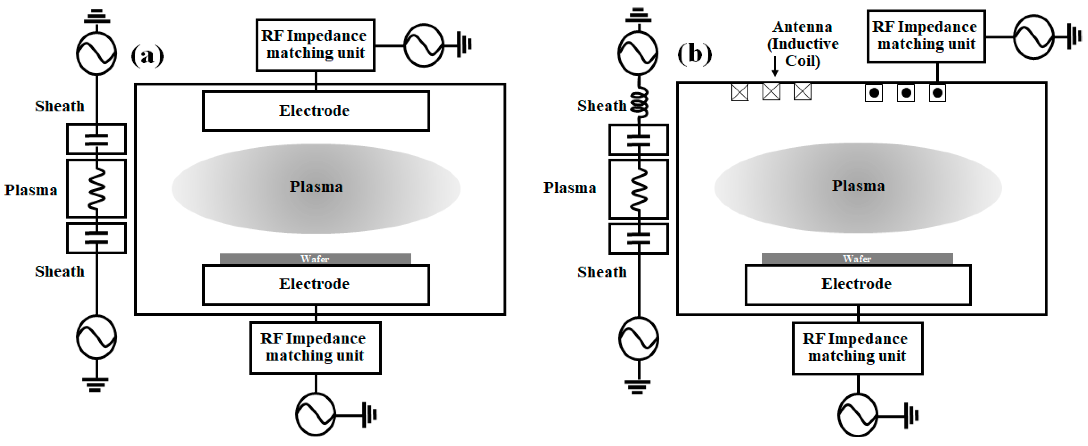
Figure 1 is a simple diagram of dual-frequency semiconductor equipment.
Figure 1a is a capacitively coupled plasma (CCP), which generates plasma using RF power to two electrodes.
Figure 1b is an inductively coupled plasma (ICP) that generates plasma by using RF power to the upper antenna (coil) and bottom electrode. RF power is supplied with a precise RF frequency and power from an external RF generator. The RF impedance matching unit reduces power loss by matching the load impedance change due to plasma to 50 Ω and helps supply constant power. Plasma is a collection of ionized gas species in a volume with external energy in a pressure condition. The plasmas in semiconductor processing can be generated by external RF power. The net movement of electrons in the plasma allows a current path between two powered electrodes in an electrical circuit model. Depending on the type of plasma generation source (e.g., inductively coupled plasma and CCP), the ionized gas species can be modeled with a resistor–capacitor and resistor–inductor dominant impedance circuit. Unlike conventional lumped elemental electrical circuits, the plasma impedance continuously changes along the degree of molecular dissociation and atomic ionization. The delivered RF power to the wafer-in-process via plasma also continuously changes. What matters is that the total amount of delivered power should be maintained consistently over consecutive individual runs to obtain a consistent process result, as shown in
Figure 1a,b. Thus, the impedance matching network is indispensable in plasma process equipment.
Electrons have a relatively smaller mass than ions; thus, they can be controlled independently using different frequencies. Previous studies showed that the electron density increases with the increasing frequency. When the bottom electrode is fixed at 2 MHz and 10–100 MHz frequency is supplied to the top electrode, the number of electrons is gradually increased. Accordingly, the number of electrons also increases as the source frequency increases [
13]. In previous studies, when the ion supplies 27 MHz to the top electrode and a frequency of 1–100 MHz to the bottom electrode, the ion density decreases as the frequency increases; however, no change is observed as the frequency increases [
14]. This confirms that electrons and ions can be controlled independently.
The ion flux and energy are essential parameters for the etch profile of the high aspect ratio. The production speed is generally fast in plasma with many ions and high energy. High plasma density, high ion flux, and large ion energy are important. The ion flux can be increased by increasing the plasma density; thus, it supplies a high frequency to the source power. A frequency of 13.56 MHz is often used as a source power. However, the ion energy is greater than the ion flux, which damages the substrate and is not used well but uses a higher frequency [
15]. A frequency of 60 MHz can increase the ion flux while reducing the ion energy to some extent. If a frequency higher than 60 MHz is supplied, a standing wave and skin effects occur, resulting in a poor plasma uniformity, which makes it difficult to make a high-aspect-ratio shape.
The frequency supplied to the bias power is often used to control the ion characteristics. Bias power is used in various ways from 400 KHz to 20 MHz, but high frequencies are not used well because the ion energy rapidly decreases when it exceeds 20 MHz [
16]. In the dual-frequency capacity coupled plasma (DF-CCP) equipment in the etch process, 2 MHz of bias power is the most common because high selectivity can be produced through ion transition. The source and bias powers affect each other. The frequency selections considered in this research are 13.56 MHz/2 MHz, 27.12 MHz/2 MHz, 40 MHz/2 MHz, and 60 MHz/2 MHz of the source/bias frequency. The 60 MHz/2 MHz combination must be investigated because it is the most preferred combination for the silicon dioxide etcher manufactured by a domestic equipment industry.
This frequency combination of RF generators belongs to a VHF. Even a small impedance change of the electrode can significantly influence the plasma. The physical size of dies decreases as the miniaturization of the semiconductor device technology continues. Consequently, the process yields at the wafer edge region became more interesting by reducing the center to edge variation. For instance, the allowable gate critical dimension variation is less than 2.4 nm in the 14 nm technology node and 0.5 nm in the next-generation 5 nm technology node. The process variation has become more important than ever. In semiconductor etch equipment, plasma is formed between two electrodes in a circular shape, and the plasma faces the surrounding wall or object with a plasma sheath, where the number of ions is much less than that in bulk plasma. Hwang et al. defined three types of plasma discontinuities between the wafer edge and the edge ring: (1) electrical discontinuity, (2) chemical discontinuity, and (3) thermal discontinuity [
17].
Electrical discontinuity leads to plasma sheath bending. The ion trajectory in the child Langmuir region is perpendicular to the plasma sheath, and the bended sheath causes the ion injection direction to yield an undesired etch pattern at the edge [
18]. The materials for the edge ring (e.g., quartz, silicon, and silicon carbide) are etch-resistive, and the etch rate of the edge ring is much retarded compared with the materials to be etched on the wafer. The bended-down electric field outside the wafer edge region (or near the edge ring region) lowers the electric field perpendicular to the wafer surface. It yields a lowered ion flux while the neutral flux increases [
19]. One may imagine that the amount of by-product and the associated ion densities on the wafer side are larger than those of the edge ring. Therefore, it causes a chemical discontinuity in case etch rate variation in the wafer edge region. In terms of temperature, the electrostatic chuck (ESC) maintains a consistent temperature during the etch, but the actual wafer surface temperature is much higher than that of the ESC under temperature control. The current etch equipment applies a temperature-controlled edge ring; however, a temperature gradient exists between the wafer edge and the edge ring [
20,
21,
22]. Although a symmetric chamber has been designed with the consideration to overcome three types of discontinuity, the variations in the current process requirement are difficult to overcome.
An electrode supplies the power required for the plasma generation and is directly connected to the wafer. Some studies focused on plasma control using these electrodes. One study controlled the current flowing through the plasma by inserting an impedance control circuit into the bottom electrode. In the DF-CCP using 60 and 13.56 MHz, impedance was created by directly inserting an impedance control circuit between the bottom electrode and the RF matching circuit. The current flowing through the plasma can be controlled, and a stable plasma can be formed [
23]. however, the impedance range is limited because the control of the two frequencies is carried out by one capacitor. The deposition process demonstrates plasma control with impedance control of the electrode. An impedance controlling circuit is included in the chamber wall and the bottom electrode to reduce the film stress and uniformity. Controlling the plasma impedance at the chamber wall reduces the plasma radiation pattern. The impedance control at the bottom electrode also improves the RF field formed by the plasma [
24]. Research was also conducted to control plasma characteristics using a resonance circuit that blocks the flow of a specific frequency in the electrode. In the CCP equipment, 2, 27, and 60 MHz were supplied to the bottom electrode, and an impedance control circuit was inserted to block a specific frequency in the top electrode. The changes in the ion density and etch rate were then checked. The uniformity of the ion density and the etch rate can be improved by blocking and passing the specific frequency signals flowing through the electrode [
25,
26]. The abovementioned results confirmed that the electrode in the CCP equipment is an essential factor affecting the etch process and plasma. However, repeating the etch process damages the electrode and changes the impedance.
3. Impedance Matching Circuit
A filter is essential for extracting the desired electrical signals by selecting the desired frequency information among various frequencies. This filter can select and cut off the frequency only by the operation characteristics and the combination of inductors and capacitors. In the semiconductor equipment, filters composed of capacitors and inductors are commonly used to protect the circuits of the semiconductor equipment components. These filters protect the RF generator by allowing only the frequency of the components that the internal circuit of the RF generator can withstand to flow. A filter is also used in a voltage–current (VI) sensor to detect the voltage and current components occurring at a specific frequency. A filter is designed using the inductor and capacitor device characteristics.
XL is the impedance according to the inductor value, and
XC is the impedance according to the capacitance. The higher the frequency, the larger the
XL value and the smaller the
XC; hence, the low-frequency signal flows well in the inductor, and the capacitors have the property of the high-frequency signal flowing well. The capacitor has a negative impedance, whereas the inductor has a positive impedance. Using this, one can adjust the total impedance of a specific circuit and the impedance of a specific frequency. Resonance is a representative example of good usage. It occurs because of the device’s charging and discharging characteristics and acts to pass or block specific frequencies. The resonant frequency is the point where the imaginary impedance becomes 0, and the following formula is satisfied:
f is the resonance frequency. Different phenomena occur depending on the arrangement. A filter uses this resonance phenomenon and the device characteristics to make the desired frequency impedance close to 0 and pass it through and can make a circuit that cuts off the unwanted frequency.
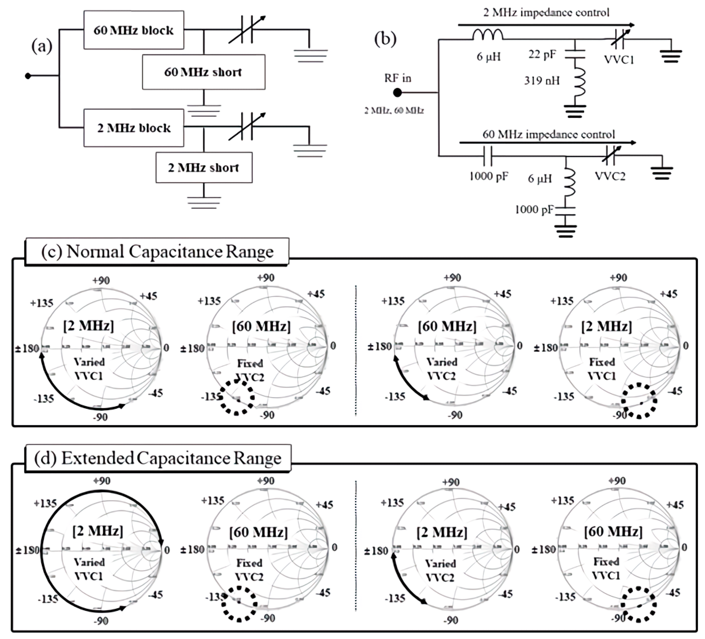
The concept of the dual-frequency RF impedance control circuit is like that of a diplexer, but the output ports are connected to VVCs for capacitance modification. The control of the VVC capacitance makes the pulse width modulation of the stepping motor connected at the end of the VVC.
Figure 2 depicts the conceptual diagram of the suggested dual-frequency RF impedance control circuit. The LC filter design requires the selection of the type of filters and the determination of the inductance and capacitance values. Considering the frequency responses of the inductor and the capacitor, the physical limitations of the inductance due to the increased parasitic capacitance from the space of the inductor coil and the capacitance were determined as 60 µH and 22–1000 pF, respectively, as a rule of thumb by RF engineers. We performed herein a stepwise circuit simulation study to have the desired impedance control circuit for the dual-frequency RF power system. RF filter circuit models were investigated with VVC1 connected to a 2 MHz signal path and VVC2 to a 60 MHz path. We investigated the crosstalk of the two signal paths within the normal capacitance range of the VVC between 100 and 1000 pF. Observing the capacitance change in the fixed capacitance of VVC2 while the capacitance of VVC1 was varied showed the impedance control functionality of the dual-frequency RF impedance matching circuits. Meanwhile, it is valuable to ensure that the circuit has no crosstalk beyond the normal operating capacitance. We also studied the extended capacitor range of VVCs from 100 to 100,000 pF.
Table 1 presents a summary of the simulation routines.
Design 1 is a simple parallel combination of an LPF for the 2 MHz signal and an HPF for 60 MHz in
Figure 3. The figures intend to demonstrate the effect of the variation of the 2 MHz VVC on the fixed 60 MHz capacitance and that of the 60 MHz VVC on the fixed 2 MHz capacitance. The interest is in the observations of the crosstalk in the fixed VVCs in the proposed circuits, which are depicted by dotted circles in the presented Smith charts and denoted by fixed VVC1 and VVC2 throughout the Smith chart figures. Design 1 shows a relatively acceptable performance with a small amount of capacitance variation of the fixed VVC2. It also, however, demonstrates a notable change in the fixed VVC1 for 2 MHz, whereas the VVC2 connected to 60 MHz varies from 100 to 1000 pF. Therefore, both 2 and 60 MHz impedance control circuits are not independently functioning with some crosstalk, and Design 1 is not suitable for controlling the dual-frequency RF impedance system.
Double-frequency blocking circuits are considered in Design 2 to alleviate the crosstalk observed in Design 1 in
Figure 4. For the 2 MHz VVC1 circuit, the high-frequency components were blocked with a very small inductance. For the 60 MHz VVC2 circuit, the low-frequency components were blocked with a very large capacitance. Additionally, by-passing band pass filters were added to the ground to quench out the undesired signals. The same simulation routine for the crosstalk visualization in both VVC2 and VVC1 was obtained. Unlike our postulation of the signal by-pass, we observed a small amount of crosstalk for both the fixed VVC2 in the normal capacitance range and the fixed VVC1 in the extended range. Thus, Design 2 may be acceptable for the dual-frequency RF matching system that requires intermediate accuracy but not suitable for the current high-end precision RF system.
Learning from the previous filter designs, the band pass filters of 2 and 60 MHz were considered in Design 3, as shown in
Figure 5, applying series resonance circuits. The corresponding impedances of the 2 MHz circuit block were −
j0.072 Ω (short) for 2 MHz and −
j2345 Ω for 60 MHz (open). The corresponding impedances of the 60 MHz circuit block were −
j3613 Ω (open) for 2 MHz and −
j0.027 Ω for 60 MHz (short). The simulation result was relatively satisfying with a negligible crosstalk in the extended capacitance range but still suffered from the cut off frequency whose impedance was lower than that obtained using parallel resonance. The impedance range may be limited if the impedance is small enough. Having a large impedance is efficient. However, the disadvantage of the band pass filter can be overcome with the band stop filter.
Design 4 presented in
Figure 6 with band stop filters was investigated with the parallel connection of an inductor and a capacitor. Allowing a 2 MHz signal transmitted by blocking 60 MHz signals for the 2 MHz control circuit, the 60 MHz impedance should be close to infinity as an open circuit, whereas the 2 MHz impedance is better when smaller. If the 60 MHz signal does not flow through the circuit, the impedance change by the influence of VVC1 is negligible. By contrast, the opposite phenomenon is expected for the 60 MHz impedance control circuit. We investigated both cases of impedance changes in the fixed VVC2 while the VVC1 was varied from 100 to 1000 pF and that in the fixed VVC1 while the VVC2 was varied from 100 to 1000 pF.
Figure 6c depicts the result. No crosstalk was observed in both cases, implying that the two parallel connected band stop filters can independently control the dual-frequency impedance circuit. The extended capacitance range of 100–100,000 pF was also tested, as shown in
Figure 6d, and the same results were achieved. We implemented the dual-frequency control circuits based on the achieved result shown in
Figure 6. The performed actual measurement is presented in the next section.


