1. Introduction
Nonlinear radars, created to help cars avoid collisions, can be traced back as far as 1973 [
1]. In comparison to the conventional linear radar, the nonlinear radar has higher immunity to clutter interference and also to the presence of metallic targets. Therefore, nonlinear radars have been utilized for several applications in the past few years [
2,
3,
4], such as wireless sensing [
5].
Most often, nonlinear radars are harmonic. Thus, the radar performance can be advanced by improving the transmitter linearity [
6], utilizing modulated waveforms for transmission [
2,
7], and improving the receiver sensitivity [
5]. On the other hand, this paper is focused on possible enhancements on the transponder end. Most nonlinear transponders are tailored to have a maximum response by attaching an appropriate antenna to the nonlinear element [
8], which is, in most cases, a Schottky diode. The used antennas are usually grounded patches [
9] or dipoles that need to be kept vertical and stiff [
10]. Therefore, designing printable single-layer transponder antennas is essential. However, connecting the antenna to the chosen diode without matching or biasing considerations introduces higher conversion loss (CL) values, which limits the reading range. In the literature, the diode is matched to the antenna either by utilizing lumped elements [
11] or using open and short circuit stubs, each necessitating a ground plane layer and occupying a large footprint [
12,
13]. Further, using lumped elements results in greater losses, as well as increased transponder weight, and that causes low acceptance in the field for identifying small objects, such as insects and small amphibians.
In the literature, having ground plane and matching with lumped elements prohibit the transponder printing, especially when utilizing the printable Schottky diodes as presented in [
14]. Thus, designing a single-layer, compact, lightweight and efficient harmonic transponder is the key issue for the full deployment of the harmonic transponders, and the main scope of this paper.
With respect to the harmonic transponder presented in the literature, it is recognized that diode conversion loss is the most crucial aspect for optimal transponder operation. However, to the best of our knowledge, no systematic analysis on the role of diode matching and biasing play in this process has been completed. We fill this gap by investigating the influence of diode matching and biasing on the transponder conversion efficiency by circuit and EM simulations besides the conducted experiments. In this regard, the paper’s advances are listed as follows:
A compact single layer harmonic transponder is introduced. This transponder outperforms the similar state-of-the-art work from the electrical size and coverage point of views as pointed out in
Table 1 of the submitted paper.
The equivalent circuit model of the introduced prototype is derived, and the circuit simulation matches very well with the EM simulation. The very good matching between the EM simulation and the circuit simulation verifies the effectiveness of the derived circuit model.
Simultaneously matching the diode at two harmonically spaced frequencies. For the harmonic transponders in the literature, the matching is addressed at only one frequency. Further, the proposed planar T-matching network is compact and does not necessitate grounded Vias for the diode matching.
Diode biasing circuit is developed, and the corresponding prototype is theoretically and experimentally verified to be compared with the proposed matching solution.
In this regard, the zero biasing HSMS-2850 Schottky diode is chosen as the nonlinear element, due to its high sensitivity and low-cost packaging. The diode barrier voltage is
, and the typical voltage and power sensitivities are at
and
, respectively. Thus, this diode is considered to be one of the most sensitive diodes at zero bias and is, thus, suitable for the employed application. The diode is matched to the antennas, using the T-matching network; thus, the transponder is of a single layer. No lumped components are used, so the weight is only limited to the diode and carrier substrate. To assess the diode CL, the equivalent transponder circuit is extracted. Moreover, biasing the diode is also elaborated upon an alternative solution to reduce the diode CL. The structure of this paper is as follows;
Section 2 introduces the proposed transponder prototype and the corresponding circuit model.
Section 3 investigates the diode conversion loss. The experimental results are demonstrated in
Section 4. Finally,
Section 5 concludes the paper.
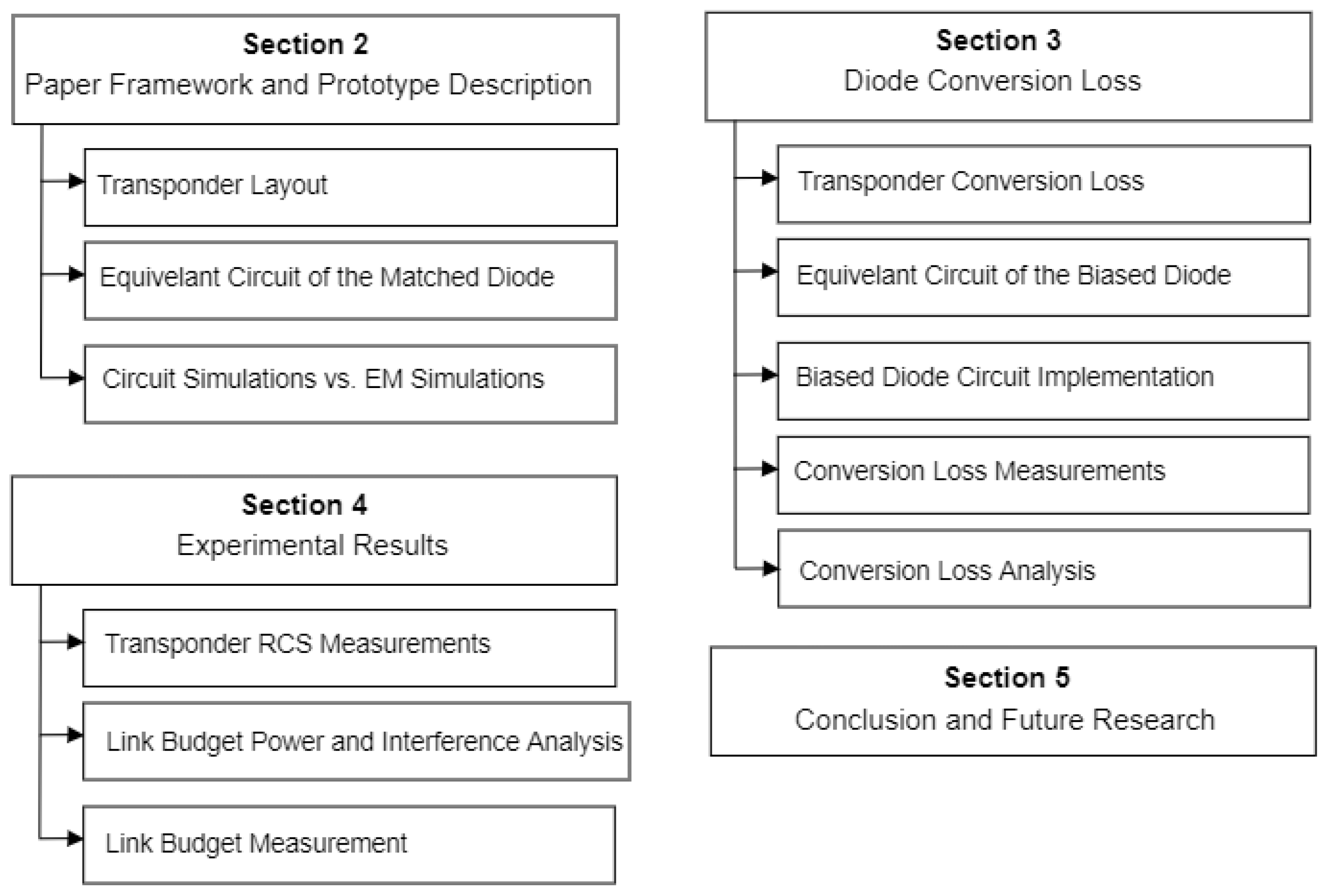
2. Paper Framework and Prototype Description
The paper is divided into five sections as explained in
Figure 1. Accordingly, the bullet points of each section are illustrated in
Figure 1.
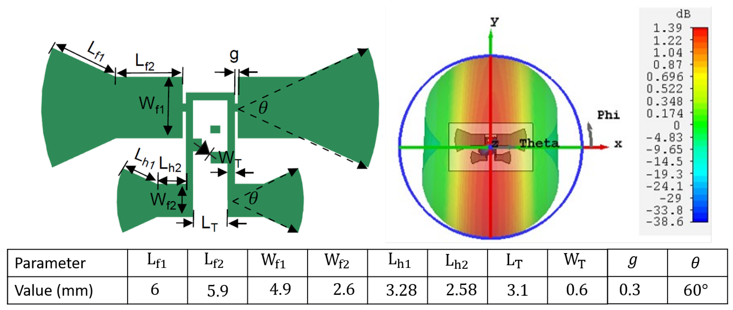
The proposed transponder consists of two bowtie dipoles placed over an Ro4350 substrate with
thickness, and the antennas are matched to the diode, using the T-matching network, as shown in
Figure 2. The two dipoles serve as transponder antennas, one for receiving
and the other, smaller one for transmitting the converted second harmonic from the diode. The realized gain of the fundamental and harmonic antennas are
and
, respectively. The transponder circuit model is driven to evaluate the matching performance at different receiving powers and frequencies.
One major design challenge is that the diode impedance is frequency and power dependent, similar to a conventional UHF RFID chip. An additional design challenge is to simultaneously match the diode impedances at two harmonically separated frequencies. In this regard, the diode is assumed to be zero biased in order to have optimized matching at the lower values of the input power, i.e., less than . Thus, the zero-biased diode impedances are calculated to be at , and at . After that, a T-matching network is utilized for simultaneously matching the diode to the dipoles at the targeted frequencies.
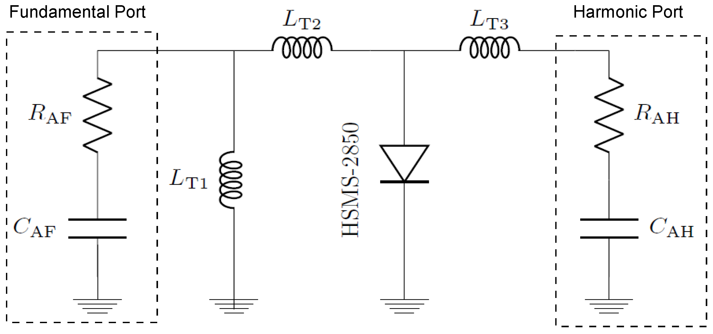
Due to the symmetry of the T-matching network, the equivalent circuit is transformed to the single-ended equivalence shown in
Figure 3, which is complete and reasonably accurate [
18]. The equivalent circuit is illustrated in
Figure 3, where
are the resistances and capacitive reactances of the fundamental and harmonic antennas, and
are the inductive reactances of the T-matching network. Therefore, the circuit element values are calculated at the fundamental frequency to be
and
, and also at the harmonic frequency to be
and
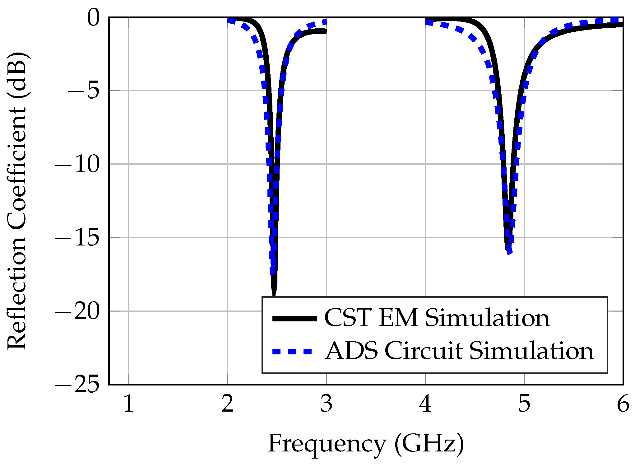
. Consequently, the very good matching between the EM simulation and circuit simulation, as shown in
Figure 4, verifies the effectiveness of the derived circuit model.
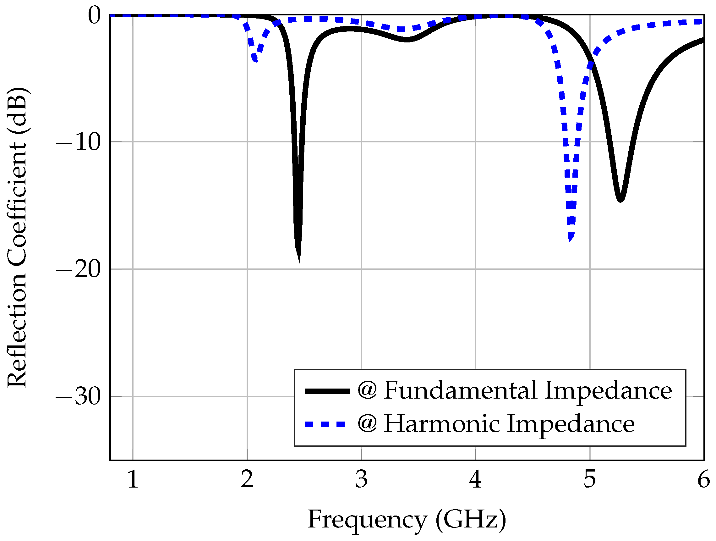
The transponder antennas are directly matched to one single differential port, which is the diode port, and the conventional two port coupling calculations are not possible. However, the reflection coefficient at the common input of the antennas can be calculated at the two different impedance states of the diode over the complete frequency span as shown in
Figure 5. Hence, considering the diode input impedance at the fundamental frequency, the reflection coefficient is found to be <
at the desired matching frequency point; however, the matching at the harmonic frequency is <
. It is likely that the same results are obtained while considering the diode input impedance at the harmonic frequency, where a matching level of less than <
is achieved at
, and a worse matching value at
, higher than <
.
3. Diode Conversion Loss
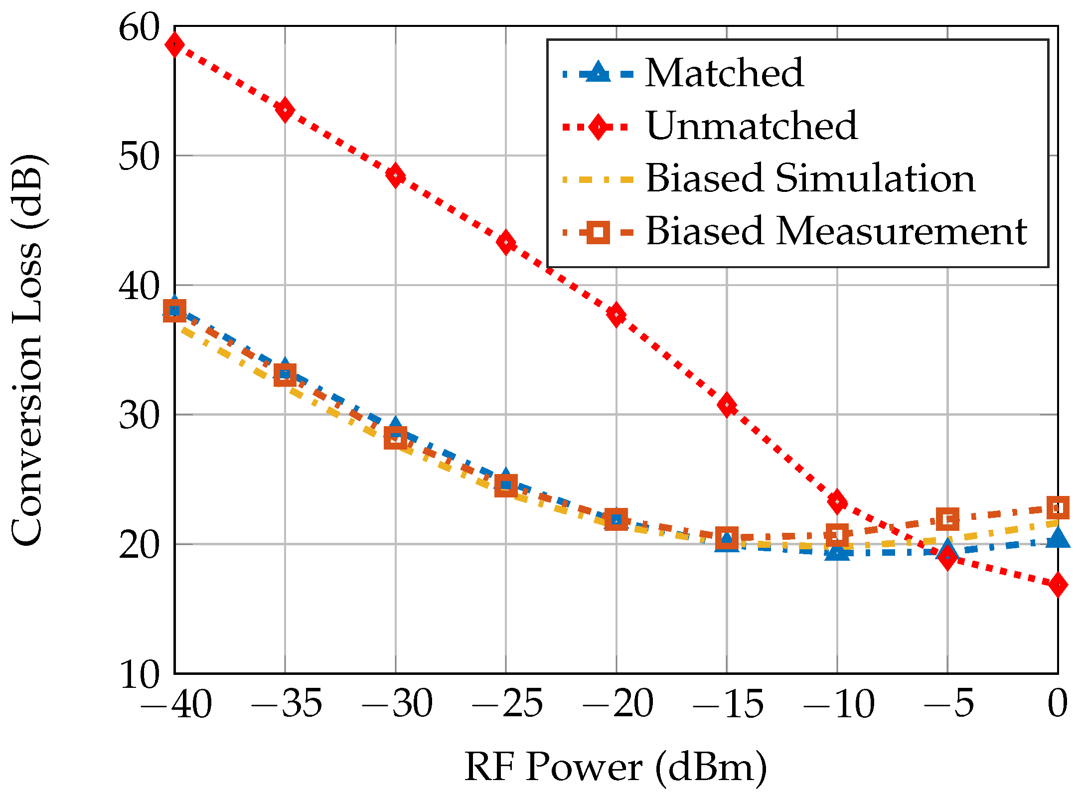
Several published papers have addressed the diode CL as a constant parameter. However, the diode CL depends on several parameters, namely, matching, frequency, and input power. Therefore, in this section, the diode CL is evaluated at different power levels, utilizing the previously developed circuit model. The CL simulation of the matched diode is performed for the developed circuit model of the introduced transponder, in which the CL illustrates that a matched diode would outperform the unmatched one by approximately if the available RF power is less than , as will be explained.
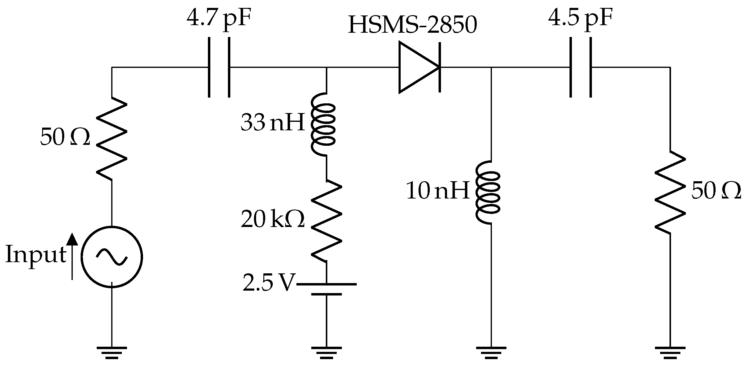
The diode biasing circuit is proposed as an alternative solution to minimize the diode CL, and the circuit parameters are designed to serve that purpose. Therefore, DC blocking capacitors can be introduced at the diode input and output along with an RF choking and DC return inductors, introduced before and after the diode, respectively. The voltage drop resistance after the battery can be utilized to maintain the optimum required biasing the diode. A rechargeable battery (ML414H) is utilized to prove the concept. However, the optimum DC-biasing voltage value for maximizing the diode-generated second harmonic components is simulated to be . Therefore, the role of the biasing circuit is also to maintain that value from the available fixed DC supply, allowing for the harvesting and maintenance of the required low DC voltage value.
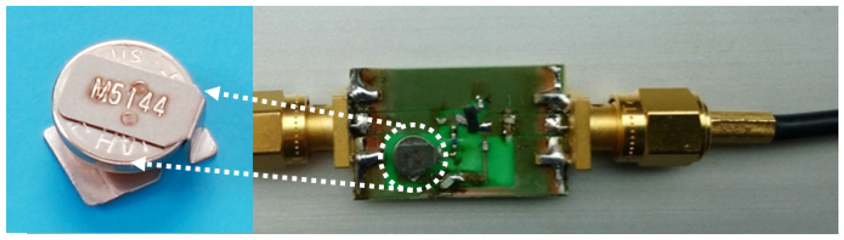
The proposed biasing circuit schematic and the corresponding implementation are explained in
Figure 6 and
Figure 7, respectively. The conversion loss of the biased diode is measured after calibrating the cables and filters losses, and the measured results verify that the biased diode CL is higher than the CL of a matched diode if the available input power is greater than
as illustrated in
Figure 8. However, a matched diode CL is lower than a biased one for an input power smaller than
as explained in
Figure 8.
The diode biasing solution would have two advantages. First, the biasing circuit can be directly connected to any standard
antennas without matching considerations. Second, the circuit would operate over a wider bandwidth, compared to the matching solution. Moreover, the optimum biasing value, which is ≈
, can be harvested from the incident wave at the expense of having an extra harvesting circuit, as presented in [
19]; thus, a completely passive solution is achievable. However, the transponder will be heavier and larger in size than the introduced narrow-band matching solution.
Diode Conversion Loss Analysis
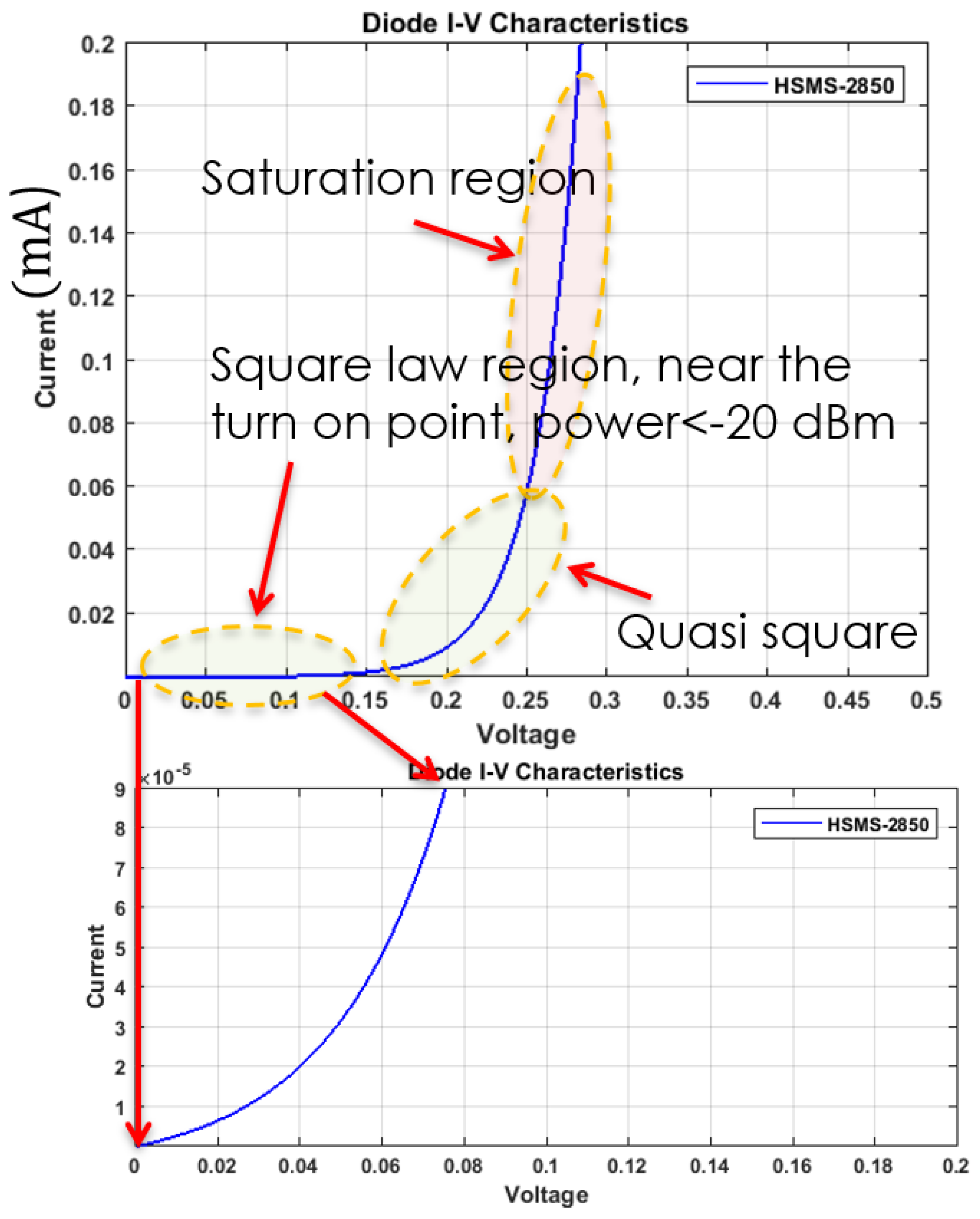
The matched transponder operation, compared to the biased one, is better understood from expression of the diode current–voltage relationship:
where
is the generated current from the diode;
,
are the diode applied and thermal voltages, respectively;
n is the diode ideality factor; and
is the diode saturation current, which is in the range of (3–5)
A. For the matched diode,
is the voltage derived from the antenna at the fundamental frequency, yielding a diode current that contains a DC component and higher frequency components, according to the Taylor expansion. To maximize the second order components generated from the diode, it has to operate in the square law region. Therefore, the main role of the matching circuit is to conceal the capacitive diode reactance and bring the diode operation to that point from the rectified diode voltage. Thus, the matched diode is self-biased from the fundamental interrogation signal, and a DC path for the generated DC component is provided by the matching network.
On the other hand, the biasing circuit brings the diode operation to that point directly from the applied DC external supply, and the optimum biasing value to maximize the second order components is found to be
, as also explained by the I–V curve shown in
Figure 9. Therefore, in
Figure 6, the conversion loss for the biased diode compared to the matched one is higher in the case of input power >
, and lower for the input power below
.
4. Experimental Results
In this section, the transponder (RCS) without diode inclusion is measured in order to verify the designed and fabricated transponder antennas. Further, the link budget measurement is conducted to prove the diode integration and the corresponding matching.
4.1. Transponder RCS Measurements
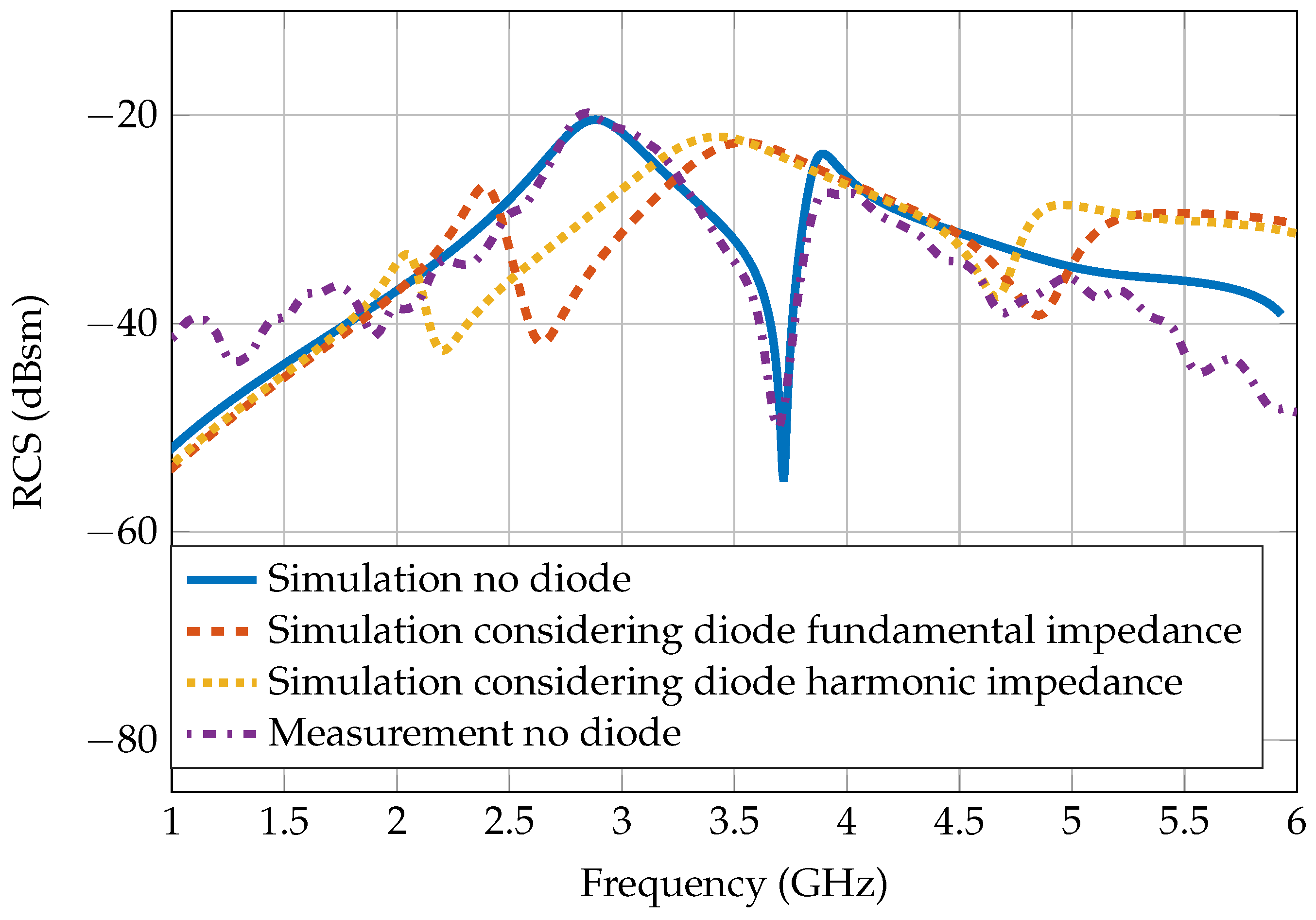
The transponder antennas are directly matched to the diode in this model, due to which the direct reflection coefficient measurement are not suitable. Alternatively, for verifying the design of transponder antennas, RCS measurement without the diode inclusion are conducted inside the anechoic chamber, where the transponder is placed on a foam substrate at a distance of
from a double ridged horn antenna that is connected to the VNA (Vector Network Analyzer). Afterwards, a calibration procedure as presented in [
20] is applied. The measured RCS frequency response is a good match with the simulated one as shown in
Figure 10, and so verifies the designed transponder antennas. Moreover, the RCS is simulated considering the diode impedance at fundamental and harmonic frequencies, where the two resonance peaks are clearly observable at the design frequencies as shown in
Figure 10.
4.2. Link Budget Power and Interference Analysis
Several wireless communication devices operate around the
frequency, including Wi-Fi, Zigbee, Bluetooth, and RFID. Therefore, these devices often interfere with each other. The effects of the coexistence of different standards in the same band are complicated and significant since the interference is spatially and temporally variant. Therefore, modeling the noise, with interference as a Gaussian component that is flat in space and time, is inaccurate when one considers interference from co-located technologies. However, this problem is addressed heavily in the literature from the protocol and communication layer perspectives [
21]. On the other hand, this paper addresses the noise and interference problem from the radar perspective. Therefore, the radar cross section (RCS) of the harmonic transponder is considered to describe its performance in a similar way to the conventional radar equation. the RCS of the harmonic transponder including the diode can be described by (
1) [
22].
where
is the harmonic transponder RCS,
is the effective area at the fundamental frequency, CL is the previously explained conversion efficiency or loss, and
,
are the realized gains of the harmonic transponder at fundamental and harmonic frequencies, respectively. According to the well-known radar equation, the received signal is explained by (
2).
where
are the gain of transmitting and receiving antennas, respectively,
is the wavelength at harmonic frequency, and
R is the transponder distance from the reader. Furthermore, to mitigate interference noise, we perform coherent averaging processing by sending
M times interrogation signals. This solution comes from the radar detection theory, and the SNR is improved by
M times, compared to noise and interference.
Link Budget Measurement
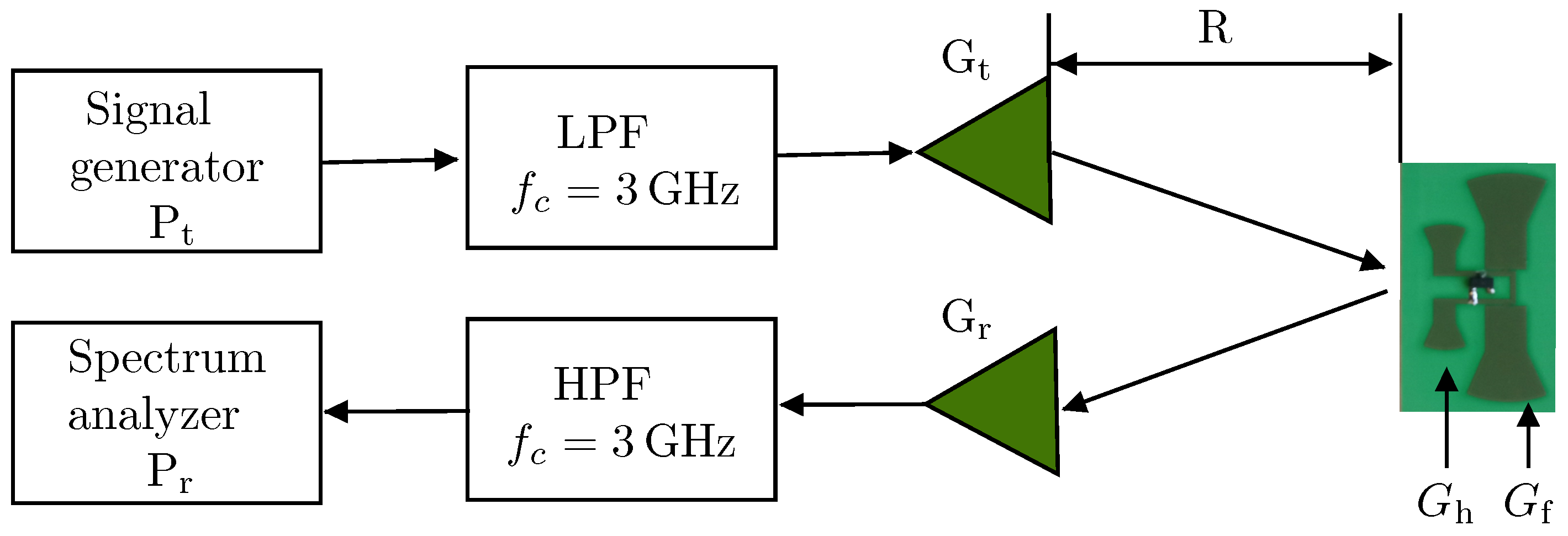
The measurement setup is explained in
Figure 11, where the transmission path consists of a signal generator with
transmitted power. The employed signal generator, which is from Keysight (N5182B MXG X-Series), is not ideal and generates harmonics with a level of
. The Low Pass Filter (LPF) is employed to suppress the transmitter generated harmonics to increase the receiver dynamic range. The same is at the receiver side—the spectrum analyzer is with the direct conversion topology—and thus, the mixer of the receiver end also produces harmonics from the received low-level fundamental signals. Thus, the High Pass Filter (HPF) is utilized to suppress the fundamental frequency at the receiver input and further increases the dynamic range.
The spectrum analyzer is set to receiving bandwidth and to intermediate frequency (IF) bandwidth with an averaging factor of 10 samples per measurement snapshot; thus, the final result represents an averaged value of 100 measurements. Therefore, a signal of up to can be detected.
The generator is connected to LPF and a Log Periodic Antenna (LPDA). The insertion loss of the cables together with the LPF is ≈
at
, and the LPDA gain is ≈
at the same frequency. The LPDA is horizontally aligned with the transponder, as shown in
Figure 11. The realized gain values of transponder antennas are ≈
and ≈
for the fundamental and harmonic frequencies, respectively. The reader receiving antenna is with ≈
gain at harmonic frequency. On the receiving path, HPF is also necessary to minimize the leakage of fundamental frequency, where the HPF insertion loss together with the cable is ≈
at the harmonic frequency. Therefore, the second harmonic at
can be detected up to
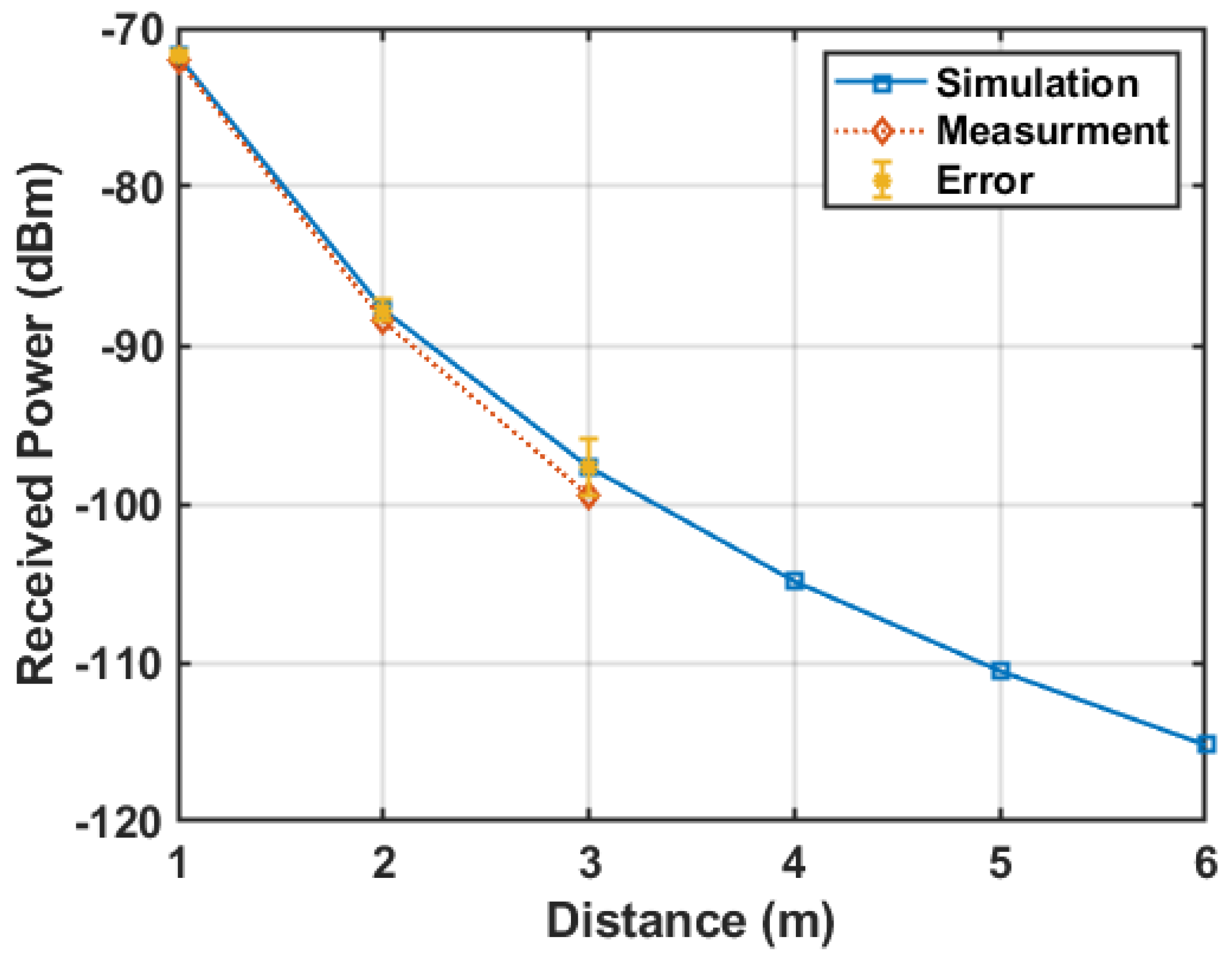
spectrum sensitivity. The range measurement verifies the link budget calculations, where a coverage of
is achieved as explained in
Figure 12.
Table 1 shows the comparison of the developed transponder versus the previously reported ones from the printability, electrical size, and coverage aspects. In comparison to transponders, which are also single layer, as listed in
Table 1, specifically, in references [
15,
17], the introduced transponder outperforms the previously mentioned contributions in terms of the electrical size and coverage point of views. Further, the other advancements compared to those in the literature are listed above.
5. Conclusions
In this paper, a novel harmonic transponder is presented. In order to efficiently convert the received fundamental frequency, the transponder receiving antenna was matched to the diode input impedance at . In addition, for efficiently transmitting the converted second harmonic, the corresponding antenna was matched at . Moreover, the CL was compared for a matched and biased diode, for which similar values of CL were achieved for both cases. However, biasing the diode does not necessitate a matching condition at the expense of having a supply voltage of ≈ and thus, more weight and volume. The introduced transponder was fabricated and a range measurement was conducted, which fit very well with the calculations. Two main research directions will be investigated in the near future. The first one is the insertion of another encoding bit to the tag structure to implement the multi-bit harmonic transponder. The second direction is the employment of the developed tags in indoor localization systems, besides the integration to the printed diode.
Author Contributions
Concept and theoretical development, M.K.; numerical analysis, M.K, A.F. and A.B., T.K.; writing of manuscript, M.K. Finally, all authors together analyzed the simulation and measurement results, discussed among themselves and completed the manuscript edition. All authors have read and agreed to the published version of the manuscript.
Funding
This research work was partially funded by the DruIde (INTERREG-PROJEKT) and the APC is funded by the Open Access Publication Fund of the University of Duisburg-Essen.
Data Availability Statement
Not applicable.
Conflicts of Interest
The authors declare no conflict of interest.
References
- Shefer, J.; Klensch, R.J. Harmonic radar helps autos avoid collisions. IEEE Spectrum 1973, 10, 38–45. [Google Scholar] [CrossRef]
- Tsai, Z.-M.; Jau, P.-H.; Kuo, N.-C.; Kao, J.-C.; Lin, K.-Y.; Chang, F.-R.; Yang, E.-C.; Wang, H. A High-Range-Accuracy and High-Sensitivity Harmonic Radar Using Pulse Pseudorandom Code for Bee Searching. IEEE Trans. Microw. Theory Tech. (TMTT) 2013, 61, 666–675. [Google Scholar] [CrossRef]
- Aumann, H.M.; Emanetoglu, N.W. A wideband harmonic radar for tracking small wood frogs. In Proceedings of the 2014 IEEE Radar Conference, Cincinnati, OH, USA, 19–23 May 2014; Volume 61. [Google Scholar]
- Mazzaro, G.J.; Martone, A.F.; Ranney, K.I.; Narayanan, R.M. A Nonlinear Radar for Finding RF Electronics: System Design and Recent Advancements. IEEE Trans. Microw. Theory Tech. (TMTT) 2017, 65, 1716–1726. [Google Scholar] [CrossRef]
- Chioukh, L.; Boutayeb, H.; Deslandes, D.; Wu, K. Noise and Sensitivity of Harmonic Radar Architecture for Remote Sensing and Detection of Vital Sign. IEEE Trans. Microw. Theory Tech. 2014, 62, 1847–1855. [Google Scholar] [CrossRef]
- Gallagher, K.A.; Narayanan, R.M.; Mazzaro, G.J.; Sherbondy, K.D. Linearization of a harmonic radar transmitter by feed-forward filter reflection. In Proceedings of the 2014 IEEE Radar Conference, Cincinnati, OH, USA, 19–23 May 2014; pp. 1363–1368. [Google Scholar]
- Polacek, V.; Pavlik, R. The use of digital modulation signals in radar system for detection of nonlinear scatterers. Int. Radar Symp. (IRS) 2011, 12, 743–747. [Google Scholar]
- Mazzaro, G.J.; Martone, A.F.; McNamara, D.M. Detection of RF Electronics by Multitone Harmonic Radar. IEEE Trans. Aerosp. Electron. Syst. 2014, 50, 477–490. [Google Scholar] [CrossRef]
- Zhu, L.; Alkhaldi, N.; Kadry, H.M.; Liao, S.; Chen, P. A Compact Hybrid-Fed Microstrip Antenna for Harmonics-Based Radar and Sensor Systems. IEEE Antennas Wirel. Propag. Lett. 2018, 17, 2444–2448. [Google Scholar] [CrossRef]
- Aumann, H.; Kus, E.; Cline, B.; Emanetoglu, N.W. A low-cost harmonic radar for tracking very small tagged amphibians. In Proceedings of the IEEE International Instrumentation and Measurement Technology Conference (I2MTC), Minneapolis, MN, USA, 6–9 May 2013; pp. 234–237. [Google Scholar]
- Rasilainen, K.; Ilvonen, J.; Hannula, J.; Viikari, V. Designing Harmonic Transponders Using Lumped-Component Matching Circuits. IEEE Antennas Wirel. Propag. Lett. 2017, 16, 246–249. [Google Scholar] [CrossRef]
- Palazzi, V.; Alimenti, F.; Mezzanotte, P.; Virili, M.; Roselli, L. Low-Power Frequency Doubler in Cellulose-Based Materials for Harmonic RFID Applications. IEEE Microw. Wirel. Components Lett. 2014, 24, 896–898. [Google Scholar] [CrossRef]
- Gu, X.; Srinaga, N.N.; Guo, L.; Hemour, S.; Wu, K. Diplexer-Based Fully Passive Harmonic Transponder for Sub-6-GHz 5G-Compatible IoT Applications. IEEE Trans. Microw. Theory Tech. 2019, 67, 1675–1687. [Google Scholar] [CrossRef]
- Neumann, K.; Kuhnel, L.; Langer, F.; Rennings, A.; Benson, N.; Schmechel, R.; Erni, D. A Stochastic Large-Signal Model for Printed High-Frequency Rectifiers Used for Efficient Generation of Higher Harmonics. IEEE Trans. Microw. Theory Tech. 2020, 68, 2151–2160. [Google Scholar] [CrossRef]
- Singh, A.; Lubecke, V.M. Respiratory Monitoring and Clutter Rejection Using a CW Doppler Radar With Passive RF Tags. IEEE Sens. J. 2012, 12, 558–565. [Google Scholar] [CrossRef]
- Palazzi, V.; Alimenti, F.; Kalialakis, C.; Mezzanotte, P.; Georgiadis, A.; Roselli, L. Highly Integrable Paper-Based Harmonic Transponder for Low-Power and Long-Range IoT Applications. IEEE Antennas Wirel. Propag. Lett. 2017, 16, 3196–3199. [Google Scholar] [CrossRef]
- Rasilainen, K.; Ilvonen, J.; Lehtovuori, A.; Hannula, J.; Viikari, V. On Design and Evaluation of Harmonic Transponders. IEEE Trans. Antennas Propag. 2015, 63, 15–23. [Google Scholar] [CrossRef]
- Zamora, G.; Zuffanelli, S.; Paredes, F.; Martin, F.; Bonache, J. Design and Synthesis Methodology for UHF-RFID Tags Based on the T-Match Network. IEEE Trans. Microw. Theory Tech. 2013, 61, 4090–4098. [Google Scholar] [CrossRef]
- Gudan, K.; Shao, S.; Hull, J.; Ensworth, J.; Reynolds, M.S. Ultra-low power 2.4 GHz RF energy Harvesting and Storage System with −25dBm Sensitivity. In Proceedings of the IEEE International Conference on RFID (RFID), San Diego, CA, USA, 15–17 April 2015; pp. 40–46. [Google Scholar]
- Alam, J.; Khaliel, M.; Fawky, A.; El-Awamry, A.; Kaiser, T. Frequency-Coded Chipless RFID Tags: Notch Model, Detection, Angular Orientation, and Coverage Measurements. Sensors 2020, 20, 1843. [Google Scholar] [CrossRef] [PubMed] [Green Version]
- Han, S.; Abu-Ghazaleh, N.B. A realistic model of co-located interference for wireless network packet simulation. In Proceedings of the 7th IEEE International Conference on Mobile Ad-hoc and Sensor Systems, San Francisco, CA, USA, 8–12 November 2010; Volume 20, pp. 472–481. [Google Scholar]
- Colpitts, B.G.; Boiteau, G. Harmonic radar transceiver design: Miniature tags for insect tracking. IEEE Trans. Antennas Propag. 2004, 52, 2825–2832. [Google Scholar] [CrossRef]
| Publisher’s Note: MDPI stays neutral with regard to jurisdictional claims in published maps and institutional affiliations. |
© 2021 by the authors. Licensee MDPI, Basel, Switzerland. This article is an open access article distributed under the terms and conditions of the Creative Commons Attribution (CC BY) license (https://creativecommons.org/licenses/by/4.0/).


