Article

Low-Process–Voltage–Temperature-Sensitivity Multi-Stage Timing Monitor for System-on-Chip Applications

Department of Electrical Engineering, Fu Jen Catholic University, New Taipei City 24205, Taiwan
*
Author to whom correspondence should be addressed.
Electronics 2021, 10(13), 1587; https://doi.org/10.3390/electronics10131587
Submission received: 7 June 2021 / Revised: 27 June 2021 / Accepted: 29 June 2021 / Published: 30 June 2021
(This article belongs to the Special Issue Advances in System-on-Chip Design)

Abstract

:
High performance and complex system-on-chip (SoC) design require a throughput and stable timing monitor to reduce the impacts of uncertain timing and implement the dynamic voltage and frequency scaling (DVFS) scheme for overall power reduction. This paper presents a multi-stage timing monitor, combining three timing-monitoring stages to achieve a high timing-monitoring resolution and a wide timing-monitoring range simultaneously. Additionally, because the proposed timing monitor has high immunity to the process–voltage–temperature (PVT) variation, it provides a more stable time-monitoring results. The time-monitoring resolution and range of the proposed timing monitor are 47 ps and 2.2 µs, respectively, and the maximum measurement error is 0.06%. Therefore, the proposed multi-stage timing monitor provides not only the timing information of the specified signals to maintain the functionality and performance of the SoC, but also makes the operation of the DVFS scheme more efficient and accurate in SoC design.

1. Introduction

With an increased demand for electronics products nowadays, the complexity of chip design in high-end electronics systems has also increased. To integrate many circuits with different functions into a single chip, the system-on-chip (SoC) implementation method is widely used in modern chip design. Currently, the improvement of semiconductors has significantly advanced the performance of chips. Thus, the operating clock frequency of systems can reach the gigahertz level. However, systems functioning at such high performance with complex SoC design can encounter several challenges. One such challenge is the delay uncertainties, such as propagation delay mismatching, clock jitter and clock skew, that degrade overall system performance and increase design efforts to meet the timing constraints. Because a large number of circuits with different functions are integrated into the SoC, these problems become significantly more serious. Additionally, the delay of the timing-critical path in the system changes due to variation in the operating environment. However, with the increased frequency of the operating clock, the time margins of the high-performance SoC become smaller, reducing the stability and performance of the chip, and can cause malfunction [1,2,3]. Furthermore, negative bias temperature instability (NBTI), hot career injection (HCI), and electromigration (EM) will also induce serious reliability issues after shipment [4]. Consequently, to ensure the functionality and performance of high-performing systems, it is necessary to develop a technology that monitors either the delay in the critical path or timing uncertainty in the circuit [1,2,3,4,5,6,7,8].
Second, because SoC has high circuit complexity, reducing overall power consumption has been an important issue in SoC design. In addition to reducing the power consumption of individual functional blocks through low-power design, using a dynamic voltage and frequency scaling (DVFS) scheme to adjust the voltage and operating frequency of specified functional blocks is a common low-power design technique in SoC [9,10]. In the DVFS technique, the main role of a timing monitor is to measure the specified timing-critical path delay in a digital block and provide such delay information to the frequency/voltage controller. Based on the measured delay provided by the timing monitor, the DVFS controller can adjust the operating frequency and supply voltage to reduce power consumption. For example, if the delay of the specified timing-critical path is larger than the system requirement, the system can decrease the operating voltage to reduce the power consumption. Conversely, if the delay of the specified timing-critical path is smaller than the system requirement, the system will increase the operating voltage to ensure the functionality of system. In the DVFS system, it is widely used a critical path replica circuit to track the delay of timing-critical path at different supply voltage [9,10,11]. Therefore, the timing monitor usually measures the delay of the critical path replica circuit. Since providing accurate timing information is key to whether DVFS can effectively reduce SoC power consumption while maintaining the functional operation, designing related monitoring circuits is crucial for SoC design.
To overcome the two aforementioned SoC design challenges, the chip should be able to monitor the critical timing. 
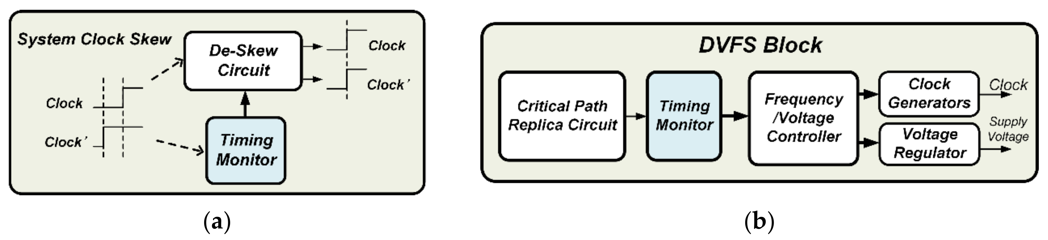
Figure 1 illustrates the role of the timing monitor in SoC. The timing-monitor monitors the timing status of specific signals in the chip, observes situations of uncertain timing, and returns the monitoring results to the control circuit of the system, which in turn prompts corresponding responses to reduce or remove the impact of timing uncertainty on the functionality of the system. For example, if the system clock skew occurs when the clock propagation delay mismatching, the timing-monitor measures and sends the phase difference between the two clock signals to the de-skew circuit to adjust the clock timing and reduce the impact of mismatched transmission delay, as shown in Figure 1a. The timing monitor is also employed in the DVFS scheme. Through the delay measurement of the critical path replica circuit, it provides the information required to adjust the voltage/frequency of the specified block to achieve the DVFS, as shown in Figure 1b. Therefore, the timing monitor is an indispensable circuit in high-performance SoC design.
Different approaches have been developed to implement a timing monitor. The simplest and most common design is the use of the delay of delay element as the monitoring resolution. The start signal propagates in the successive delay elements and the stop signal registers the state of the delay elements, which reveals the number of elements between the start and stop [12]. This design concept is very straightforward; however, its quantization resolution is limited by the delay element that is not sufficient for advance system applications. In order to improve the monitoring resolution, the Vernier delay line (VDL) structure has been proposed to achieve high delay resolution. However, such circuits have large hardware costs, and their delay resolutions are sensitive to supply-voltage variations [13]. To improve monitoring resolution and range, the structure that combines a pseudo-differential ring oscillator and a counter has been proposed [14,15]. This design can provide better monitoring resolution and range; however, the monitoring resolution is sensitive to PVT variation. Ref. [5] uses a cascading structure to improve the monitoring resolution, and takes two delay lines to lower the sensitive to supply voltage variations by choosing the suitable the width and length of each metal-oxide-semiconductor (MOS) in two delay lines. However, it is not only hard to obtain the suitable the width and length of MOS, but also hard to lower the sensitive to process and temperature variations.
Most SoC applications require several design considerations for time monitors, including measurement resolution, range, and measurement response time. The measurement resolution and range determine the accuracy and applicable range of the timing measurement results, respectively. Due to differences in the required timing monitor in the system, designing a high measurement resolution and wide range simultaneously is essential. Additionally, since DVFS applications need current timing status, the measurement response rate of the timing monitor is an important basis for judging whether the timing monitor is suitable for SoC applications. Furthermore, if the output results of the timing monitor are affected by process–voltage–temperature (PVT) variations, the reliability and stability of the timing monitor will be degraded. Therefore, this paper proposes a timing monitor that achieves high measurement resolution and wide measurement range, and low PVT variation sensitivity.
This paper is organized as follows: Section 2 describes the architecture and operating principle of the proposed timing monitor. Section 3 describes the detailed circuit of each block in the timing monitor. Section 4 presents chip implementation and experimental results. Finally, Section 5 is the conclusion.

2. Timing-Monitor Architecture

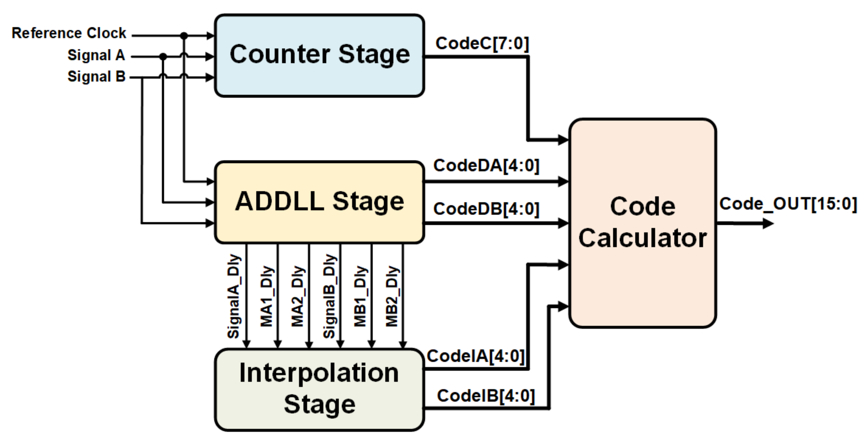
To achieve a high time-monitoring resolution and range simultaneously, a multi-stage timing-monitor architecture is proposed. Figure 2 shows the proposed timing-monitor architecture, including a code calculator and three measurement stages, namely, a counter stage, an all-digital delay-locked loop (ADDLL) stage, and an interpolation stage. These three measurement stages each have different measurement resolutions and ranges, and the overall timing-monitoring range can be expanded and resolution effectively improved when properly connected. The counter stage has the widest time-monitoring range, followed by the ADDLL stage and lastly, the interpolation stage. Conversely, the interpolation stage has the highest time-monitoring resolution, followed by the ADDLL stage and then the counter stage.
The concept of a multi-stage timing monitor is speeding the conversion rate by parallel sampling processing while considering the monitoring range and resolution. 
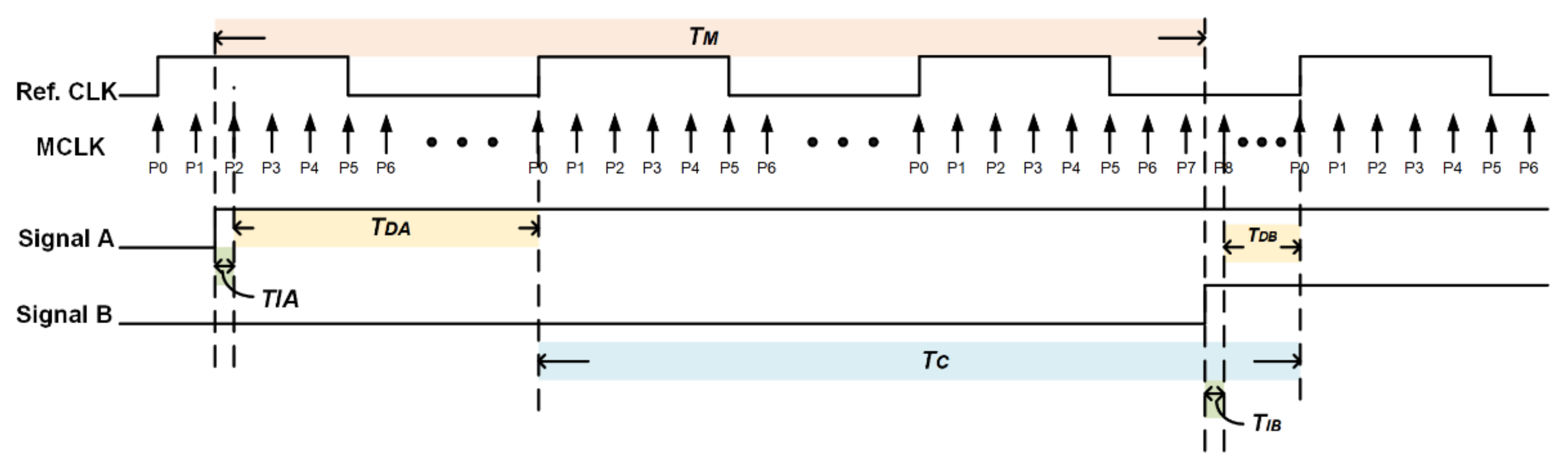
Figure 3 is an operation sequence diagram of the proposed multi-stage timing monitor. TM is the time interval to be measured and is the time difference between the positive edge of Signal A and the positive edge of Signal B. The counter stage uses the period of the reference clock (Tref) as the quantization unit to measure TM. TC is the time interval measured by the counter stage. The counter stage measures from the first positive edge of the reference clock after the positive edge of Signal A, and ends at the first positive edge of the reference clock after the positive edge of Signal B. Because the positive edges of the reference clock are not aligned with that of Signal A and Signal B, TM is not equal to TC.
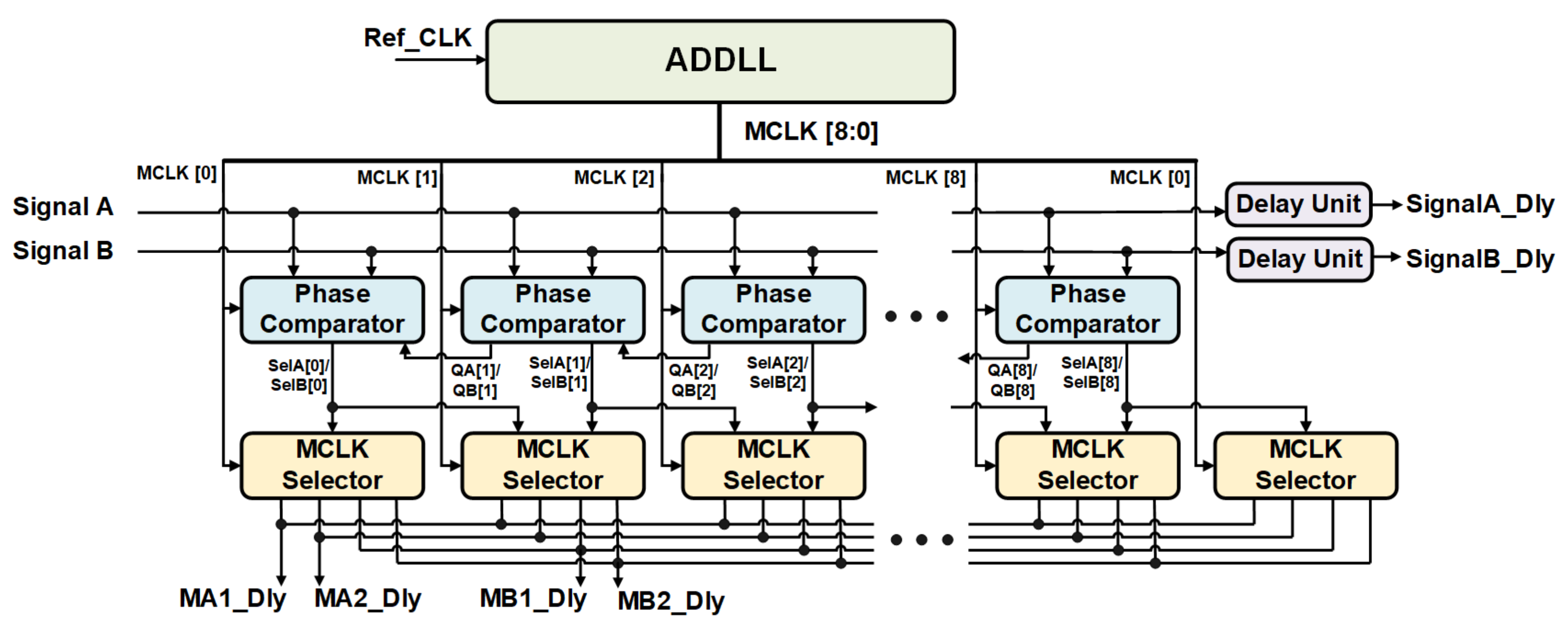
ADDLL generates multi-phase clock signals (MCLK), and its phase differences are equal and their sum equals Tref. TDA is the time interval between the positive edge of the first MCLK after the positive edge of Signal A and the first positive edge of reference clock after the positive edge of Signal A. TDB is the time interval between the positive edge of the first MCLK after the positive edge of Signal B and the first positive edge of reference clock after the positive edge of Signal B. TIA is the time interval between the positive edge of Signal A and the positive edge of the first MCLK after the positive edge of Signal A, and TIB is the time interval between the positive edge of Signal B and the positive edge of the first MCLK after the positive edge of Signal B. Since the time interval to be measured is not the same as the time interval measured by the counter stage, the part (TDA + TIA), not measured by the counter stage must be filled and the excesses (TDB + TIB) deducted. Thus, the time interval to be measured can be expressed as
TM = (TDA + TIA) + TC − (TDB + TIB)
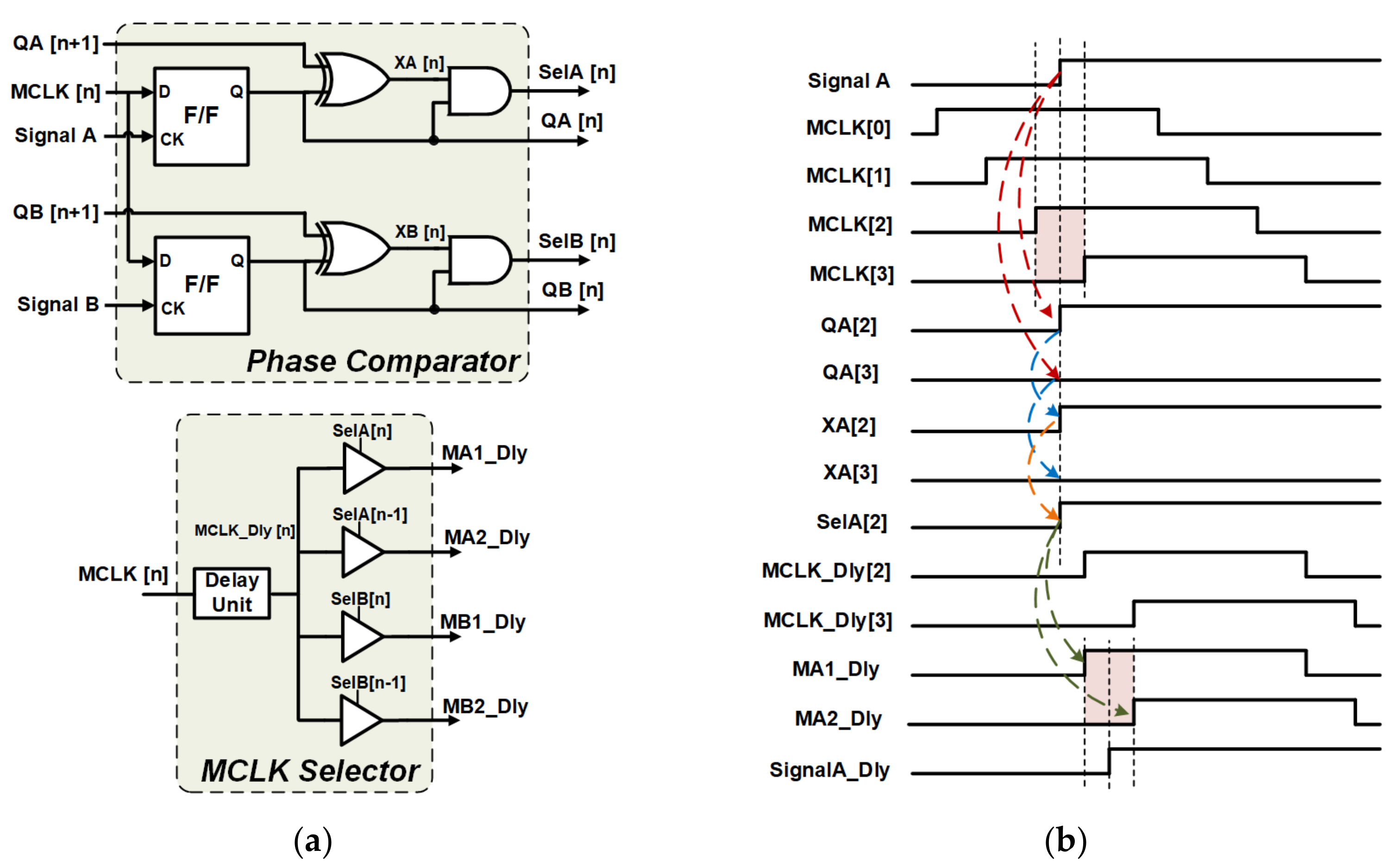
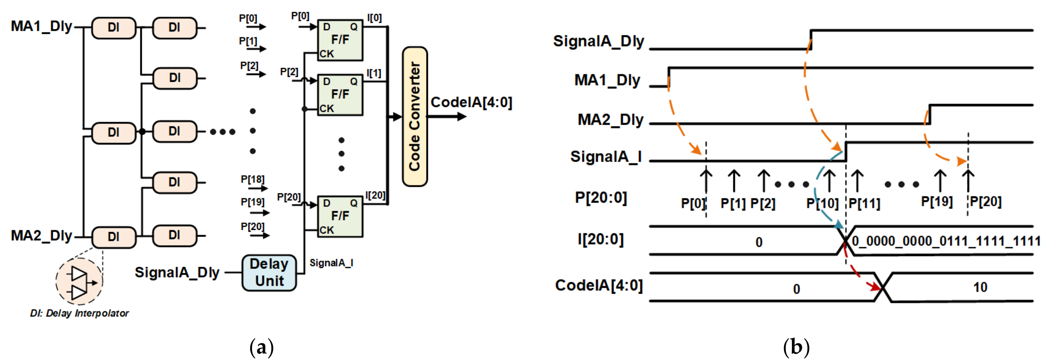
The counter stage measures TC and converts it to output digital code CodeC. TDA and TDB are measured using the ADDLL stage and obtaining the digital codes CodeDA and CodeDB, respectively. TIA and TIB are measured by the interpolation stage and obtaining the digital codes CodeIA and CodeIB, respectively. When all three stages are measured completely, the output codes of each stage are sent to the output code calculator for integrated calculation, and the final output code can be obtained. ADDLL selects two adjacent MCLKs (MA1 and MA2) of the positive edge of Signal A to generate CodeDA. These signals are sent to the interpolation stage for more accurate measurement. Similar to Signal A, ADDLL also selects two adjacent MCLKs (MB1 and MB2) of the positive edge of Signal B to generate CodeDB, and these signals are sent to the interpolation stage for more accurate measurement. However, since the positive edges of Signal A and B only appear one time during the measurement, the interpolation stage cannot measure in time. Therefore, the ADDLL stage retains the time relationship between Signal A, MA1, and MA2 through delay to ensure the correctness of the input signal of the interpolation stage. Signal A_Dly, MA1_Dly, and MA2_Dly are the delay signals corresponding to Signal A, MA1, and MA2, respectively. Similar to Signal B, the ADDLL stage also generates Signal B_Dly, MB1_Dly, and MB2_Dly through an appropriate delay as input signals for the interpolation stage.
Because the first stage uses a counter for measurement, it achieves a wider measurement range by increasing the number of counter bits. Compared with counter and ADDLL stages, the interpolation stage has a higher measurement resolution, and since the measurement resolution of the overall timing monitor is determined by the interpolation stage, the measurement resolution of the timing monitor improves significantly. Therefore, the proposed multi-stage timing monitor achieves high measurement resolution and a wide measurement range concurrently.
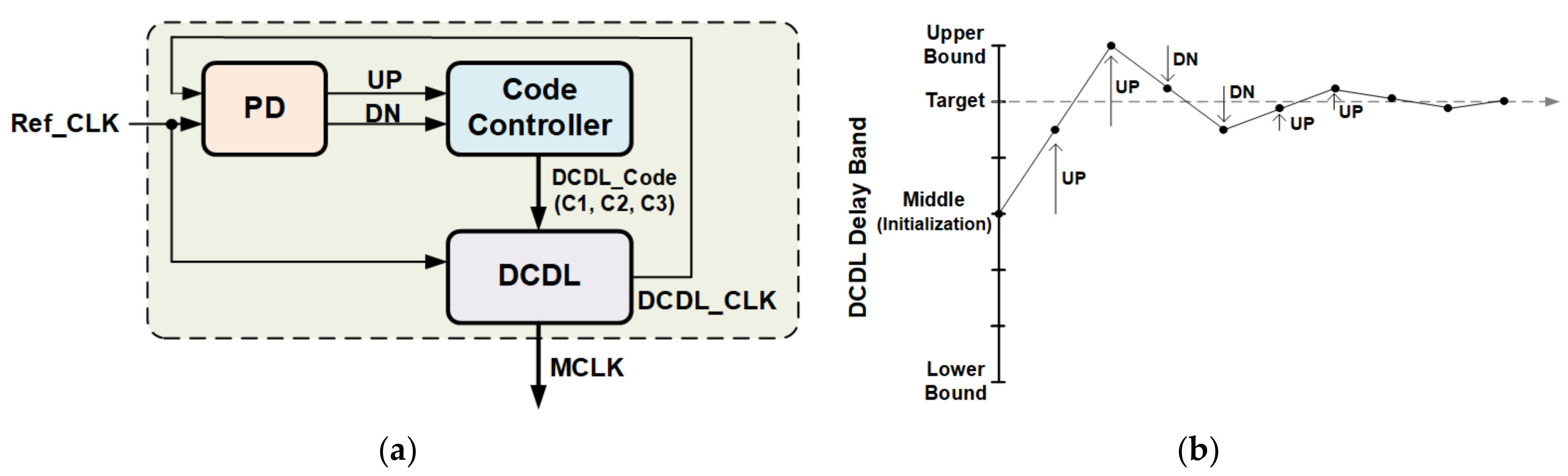
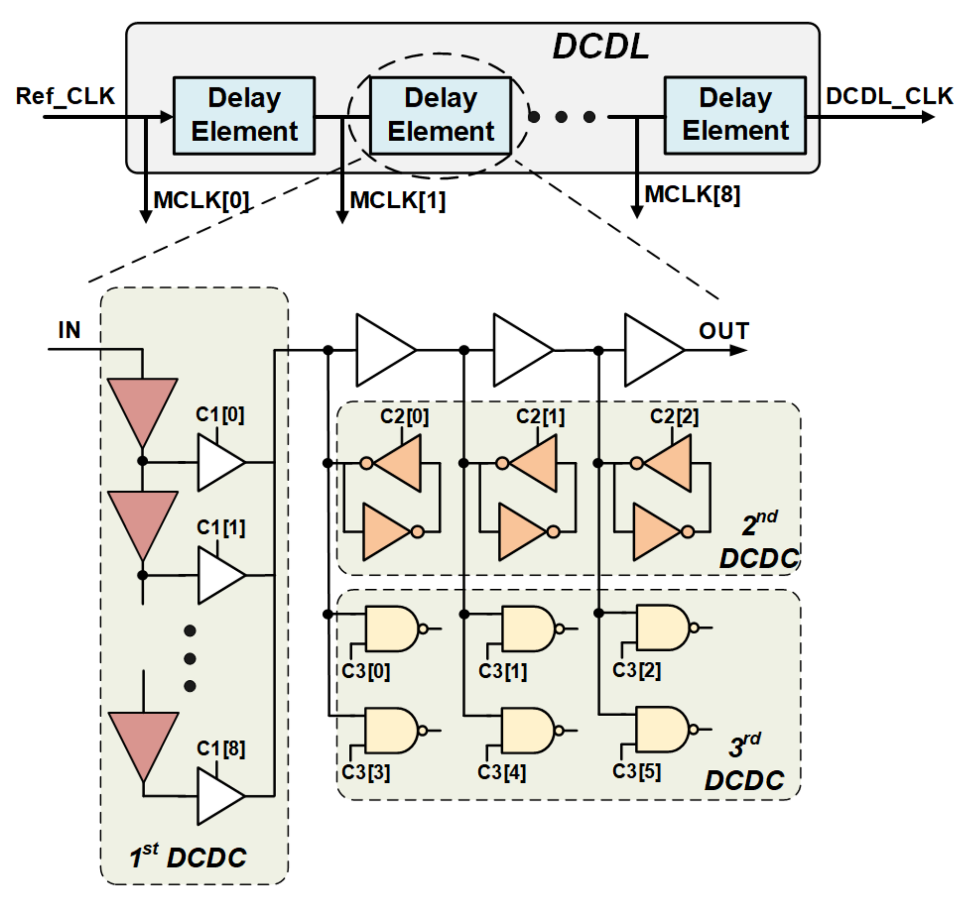
The MCLKs are generated using the digitally-controlled delay line (DCDL) in the ADDLL, and the time interval between two adjacent MCLKs equals the delay of the delay element (DE) in the DCDL. The overall delay of DCDL equals Tref when ADDLL is locked. If there are M DEs in the DCDL, the delay of each DE, which is the measurement resolution of the ADDLL stage, is 1/M of Tref. So long the reference clock cycle remains stable, the delay of the DE does not change due to PVT variations, thus reducing the sensitivity of measurement resolution of ADDLL stage to the environmental variation and its measurement resolution keeps 1/M of the counter stage. Furthermore, if the delay of DE is equally divided into N parts, the measurement resolution of the interpolation stage is one-Nth of the ADDLL stage. Therefore, the overall timing measurement is expressed as
TM = [(CodeC × M × N) + (CodeDACodeDB) × N + (CodeIACodeIB)] × ΔTI
ΔTI is the measurement resolution of the interpolation stage. Added to high measurement resolution and wide measurement range, the measurement resolution of each stage of the proposed architecture is unaffected by PVT variations and can maintain a fixed proportional relationship, effectively reducing the sensitivity of time-monitoring results to environmental variations. The detailed circuit of each stage will be described in the following sections.

3. Circuit Design

3.1. ADDLL Stage

The ADDLL consists of a phase detector (PD), a code controller, and a DCDL, as shown in Figure 4a. PD receives two clock signals of the reference clock (Ref_CLK) and DCDL output (DCDL_CLK) and generates the input signal of the code controller (UP and DN) from the phase relationship between these two clock signals. The code controller adjusts the DCDL control code (DCDL_Code) from UP and DN and then changes the delay of DCDL by changing the DCDL control code. By aligning the positive edges of the Ref_CLK and DCDL_CLK, ADDLL is locked, meaning that the delay of DCDL equals Tref. The code controller uses binary search to control the code-locking process [16]. Figure 4b illustrates the binary search-locking procedure. First, the DCDL control code is set to an intermediate value. When UP or DN is at a high level, the DCDL control code increases or decreases by a specific amount of change. If the output of the PD changes from UP to DN or vice versa, the change of DCDL control code reduces to halve. Finally, when the change is reduced to one, the binary search process is completed, and ADDLL also completes the locking procedure.
Figure 5 shows the circuit block diagram of DCDL containing nine DEs. Each proposed cascading-stage DE consists of three delay stages, namely, first, second, and the third digitally-controlled delay cell (DCDC). These three DCDC have different controllable delay range and resolution. The first has the widest controllable delay range, followed by the second and then the third DCDC. Conversely, the third has the finest controllable delay resolution, followed by the second and then the first. The overall controllable delay range and resolution of cascading-stage DE is a function of the first and third DCDC, respectively. Thus, the advantage of cascading-stage structure DE is that can provide a wide controllable delay range and fine controllable delay resolution.
The first DCDC consists of nine delay buffers with output connected to a tri-state buffer. It selects one of nine signal propagation paths through the one-hot encoding control signals (C1) to generate different delays. Also, its controllable delay range can be enlarged easily by increasing the number of delay buffers. However, the controllable delay resolution of the first DCDC only equals the delay of one delay buffer. Therefore, the second DCDC improves the overall controllable delay resolution of DE. It consists of three cross-coupled circuits composed of an inverter and a tri-state inverter. Given the enabled signal of the tri-state inverter at a high level, a current opposite to the direction of the signal propagation is generated instantaneously as the signal transition, which changes the delay of the second DCDC. Therefore, the control signal of the second DCDC (C2) changes the delay of DE. To further improve the overall resolution of DE, the third DCDC, composed of 6 two-input NAND gates, is added to DE. The gate capacitance of the two-input NAND gate slightly changes through different logical levels of control code (C3), thereby changing the delay of DE.
For these three DCDCs to have a better connection and to ensure that the finest controllable delay resolution of DE is the same as the controllable delay resolution of the third DCDC, the controllable delay range of each DCDC should be greater than the controllable delay resolution of the previous DCDC [17] (Table 1).
Figure 6 shows the circuit diagram of the complete ADDLL stage, including an ADDLL, nine phase comparators, ten MCLK selectors, and two delay units. The phase comparators provides the selection signals required by the MCLK comparator. From these selection signals (SelA[8:0] and SelB[8:0]), the MCLK selectors select two adjacent MCLKs on the positive edge of Signal A and Signal B, respectively. Through an appropriate delay, the delayed Signal A and B and their respective MCLKs (Signal A_Dly, MA1_Dly, and MA2_Dly) and (Signal B_Dly, MB1_Dly, and MB2_Dly) are sent to the interpolation stage for more accurate measurement.
The phase comparator has two blocks of circuits for Signal A and B, respectively, each block consists of a D flip–flop and some logic gates, as shown in Figure 7a. The operation waveform of the phase comparator and MCLK selector is illustrated in Figure 7b. The D flip–flop judges the phase relationship between Signal A/Signal B and MCLK. If the positive edge of MCLK leads to the positive edge of Signal A/Signal B, the output of D flip–flop (QA[8:0]/QB[8:0]) is high, otherwise, the output is low. Then, an exclusive-OR gate finds which flip–flop output differs from the adjacent result, so the MCLK selection signal can be obtained. Because more than one output of XOR gate is high level within a reference clock cycle, to avoid malfunction, a two-input AND gate are used to obtain the correct MCLK selection signal.
The circuit diagram of the MCLK selector is shown in Figure 7a. To ensure the correct MCLK selection signal appears earlier than MCLKs, MCLKs generates a delayed version signal through a delay unit. The MCLK selector receives the MCLK selection signal and decides which delayed version of MCLK is sent to the interpolation stage. Signal A and Signal B also pass through the same delay unit, maintaining the relative timing relationship with the selected MCLKs. Here, an example that explains the operation of the phase comparator and MCLK selector is used. If the positive edge of Signal A lies between the positive edges of MCLK[2] and MCLK[3], then QA[2] is the high level and QA[3] is the low level. Consequently, the output of the XOR gate (XA[2]) changes to a high level, and the MCLK selection signal (SA[2]) changes to a high level. Thus, the delayed version of MCLK[2] and MCLK[3] are MA1_dly and MA2_dly, respectively.

3.2. Interpolation Stage

The interpolation stage mainly measures the time interval between selected MCLKs and Signal A/Signal B using multiple sampling signals between adjacent MCLKs to improve measurement accuracy. Delay interpolation makes the time interval between multiple sampling signals equal [16]. Figure 8a shows the circuit diagram of the interpolation circuit. There are two interpolation circuits in the interpolation stage, one for Signal A, the other for Signal B. Each interpolation circuit generates 21 sampling signals (P[20:0]) using delay interpolator, and then uses D flip-flops to generate the interpolation stage output. For example, if the positive edge of Signal A lies between P[10] and P[11], all bits of the outputs of D flip–flop I[10:0] are 1 and those of I[20:11] are 0. Finally, the code converter converts the outputs of a D flip–flop (I[20:0]) to the CodeIA[4:0] with binary format, as shown in Figure 8b.

3.3. Code Calculator

When the three measurement stages complete the measurements, the results are sent to the code calculator for integrated calculation following Equation (2). Because ADDLL divides Tref into 9 MCLKs with equal time intervals, M equals 9. Additionally, since the interpolation stage divides the time interval between adjacent MCLKs into 20 equal intervals, N is equal to 20. The code calculator uses simple multipliers and adders to complete the calculation of the output code. For example, if CodeC[7:0], CodeDA[4:0], CodeDB[4:0], CodeIA[4:0], and CodeIB[4:0] equals 100, 8, 3, 18, and 16, respectively, the output code (Code_OUT[15:0]) equals 18102 (100 × 180 + 5 × 20 + 2 × 1). The system obtains the ΔTI from the known Tref, and then uses the output code to get the time interval to be monitored.

4. Experimental Results and Discussion

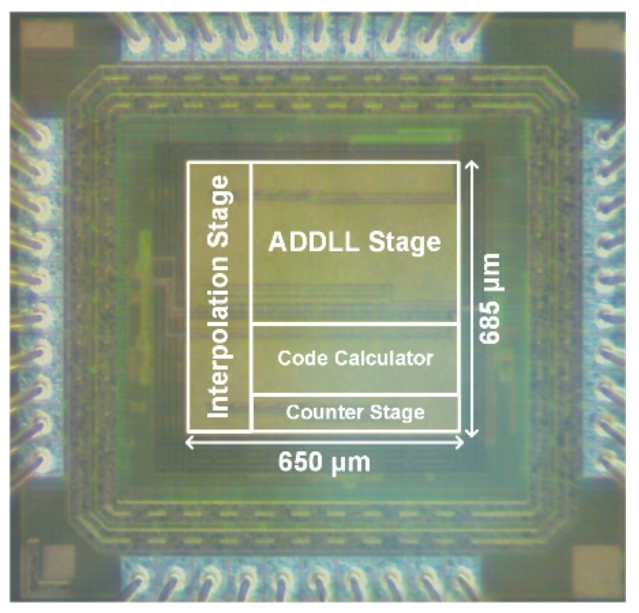
The proposed timing monitor is designed and implemented through the mixed-signal design flow, and fabricated by TSMC 0.18 µm 1P6M CMOS standard process with a core area of 685 µm × 650 µm. Figure 9 shows the microphotographs of the chip. The post-layout simulation results of the proposed timing monitor verify the relationship between the input time interval and output digital code. The range and resolution of the proposed timing monitor are 2.2 µs and 47 ps, respectively. The power consumption of the timing monitor is 7.58 mW when the reference clock signal frequency is 120 MHz and the operating voltage is 1.8 V.
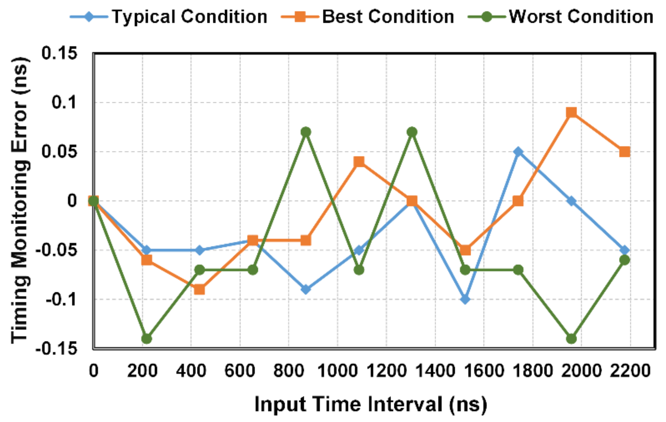
To verify the impact on the output results under different PVT conditions, Figure 10 shows the timing measurement errors under three operation conditions. The process corner, supply voltage, and operating temperature of the best condition are Fast/Fast, 1.98 V, and −40 °C, respectively. Those for the typical condition are Typical/Typical, 1.8 V, and 25 °C, respectively and for the worst condition, we have Slow/Slow, 1.62 V, and 125 °C, respectively. The maximum monitoring error of the best, typical, and worst conditions is 0.02%, 0.02%, and 0.06%, respectively. Since there is the phase error between reference clock and DCDL output when ADDLL is locked, the monitoring resolution of the ADDLL stage is not equal to 1/M of Tref. Additionally, the outputs of interpolation stage may be not stable due to the charge and discharge current mismatching of interpolation circuit These errors cause the overall timing monitoring error is not the same with different input time interval.
Table 2 provides the performance comparisons with the state-of-the-art timing-monitor design. From Table 2, the proposed timing monitor has the best timing-monitoring resolution compared to other designs, and therefore provides more accurate timing measurement results for SoC applications. Additionally, it provides various time monitoring and can be widely used in various time monitoring applications. If the system requires a wider time-monitoring range, it needs only increase the output bit of the counter to meet the requirements of the system. Furthermore, compared with previous designs, it has a lower sensitivity to PVT variations and greatly improves the stability of the output. In sum, the proposed timing monitor not only can provide a finer timing-monitoring resolution and a wider timing-monitoring range but also achieve a lower PVT-variations sensitivity, thus it is suitable for SoC applications.

5. Conclusions

This paper presents a structured multi-stage timing monitor for SoC applications comprising three time monitor stages to achieve wide-range, high-resolution time monitoring, obtain accurate time-monitoring results, and more easily meet system requirements for time monitoring. Additionally, due to the low PVT sensitivity of the proposed design, it has high stability in SoC with high complexity with variable operating environments. Therefore, the proposed timing monitor not only effectively reduces the impact of uncertain timing on the system but also makes the operation of the DVFS scheme more efficient and accurate in high performance and complex SoC design.

Author Contributions

D.S. designed the research and wrote the manuscript; H.-R.L. and L.T. collected the experimental data. All authors have read and agreed to the published version of the manuscript.

Funding

This project was supported in part by the Ministry of Science and Technology of Taiwan, under Grant MOST 109-2221-E-030-016-MY2.

Acknowledgments

The authors thank the EDA tool support and chip fabrication of the Taiwan Semiconductor Research Institute.

Conflicts of Interest

The authors declare no conflict of interest.

References

  1. Jansson, J.-P.; Keränen, P.; Jahromi, S.; Kostamovaara, J. Enhancing Nutt-based time-to-digital converter performance with internal systematic averaging. IEEE Trans. Instrum. Meas. 2020, 69, 3928–3935. [Google Scholar] [CrossRef] [Green Version]
  2. Pei, S.; Li, H.; Li, X. A high-precision on-chip path delay measurement architecture. IEEE Trans. Very Large Scale Integr. (VLSI) Syst. 2012, 20, 1565–1577. [Google Scholar] [CrossRef]
  3. Jain, A.; Veggetti, A.; Crippa, D.; Rolandi, P. On-chip delay measurement circuit. In Proceedings of the 17th IEEE European Test Symposium (ETS), Annecy, France, 28–31 May 2012. [Google Scholar]
  4. Iizuka, T.; Asada, K. All-digital PMOS and NMOS process variability monitor utilizing shared buffer ring and ring oscillator. IEICE Trans. Electron. 2012, E95-C, 627–634. [Google Scholar] [CrossRef]
  5. Sheng, D.; Hung, Y.C. Wide-range and high-resolution on-chip delay measurement circuit with low supply-voltage sensitivity for SoC applications. Rev. Sci. Instrum. 2016, 87, 116101. [Google Scholar] [CrossRef] [PubMed]
  6. Drake, A.; Senger, R.; Deogun, H.; Carpenter, G.; Ghiasi, S.; Nguyen, T.; James, N.; Floyd, M.; Pokala, V. A distributed critical-path timing monitor for a 65 nm high-performance microprocessor. In Proceedings of the IEEE International Solid-State Circuits Conference (ISSCC), San Francisco, CA, USA, 11–15 February 2007. [Google Scholar]
  7. Wang, J.-S.; Wei, S. Temperature-variation-aware design and comparative study of transition-detector-based error-detecting latches for timing-error resilient pipelined systems. IEEE Trans. Very Large Scale Integr. (VLSI) Syst. 2017, 25, 2893–2906. [Google Scholar] [CrossRef]
  8. Machado, R.; Cabral, J.; Alves, F.S. All-digital time-to-digital converter design methodology based on structured data paths. IEEE Access 2019, 7, 108447–108457. [Google Scholar] [CrossRef]
  9. Jia, T.; Joseph, R.; Gu, J. An adaptive clock management scheme exploiting instruction-based dynamic timing slack for a general-purpose graphics processor unit with deep pipeline and out-of-order execution. In Proceedings of the IEEE International Solid-State Circuits Conference (ISSCC), San Francisco, CA, USA, 17–21 February 2019. [Google Scholar]
  10. Das, S.; Roberts, D.; Lee, S.; Pant, S.; Blaauw, D.; Austin, T.; Flautner, K.; Mudge, T. A self-tuning DVS processor using delay-error detection and correction. IEEE J. Solid-State Circuits 2006, 41, 792–804. [Google Scholar] [CrossRef]
  11. Nishizawa, S.; Ishihara, T.; Onodera, H. An impact of process variation on supply voltage dependence of logic path delay variation. In Proceedings of the VLSI Design, Automation and Test (VLSI-DAT), Hsinchu, Taiwan, 27–29 April 2015; p. 14. [Google Scholar]
  12. Rashidzadeh, R.; Muscedere, R.; Ahmadi, M.; Miller, W.C. A delay generation technique for narrow time interval measurement. IEEE Trans. Instrum. Meas. 2009, 58, 2245–2252. [Google Scholar] [CrossRef]
  13. Rashidzadeh, R.; Ahmadi, M.; Miller, W.C. An all-digital self-calibration method for a vernier-based time-to-digital converter. IEEE Trans. Instrum. Meas. 2010, 59, 463–469. [Google Scholar] [CrossRef]
  14. Braga LH, C.; Gasparini, L.; Grant, L.; Henderson, R.K.; Massari, N.; Perenzoni, M.; Stoppa, D.; Walker, R. A fully digital 8 16 SiPM array for PET applications with per-pixel TDCs and real-time energy output. IEEE J. Solid-State Circuits 2014, 49, 303–314. [Google Scholar] [CrossRef]
  15. Manuzzato, E.; Gasparini, L.; Perenzoni, M.; Zou, Y.; Parmesan, L.; Battistoni, G.; De Simoni, M.; Dong, Y.; Fischetti, M.; Gioscio, E.; et al. A 16×8 digital-SiPM array with distributed trigger generator for low SNR particle tracking. IEEE Solid-State Circuits Lett. 2019, 2, 75–78. [Google Scholar] [CrossRef]
  16. Chung, C.-C.; Hou, C.-Y. An all-digital delay-locked loop for 3-D ICs die-to-die clock deskew applications. Microelectron. J. 2017, 70, 63–71. [Google Scholar] [CrossRef]
  17. Sheng, D.; Chen, W.Y.; Huang, H.T.; Tai, L. Digitally controlled oscillator with high timing resolution and low complexity for clock generation. Sensors 2021, 21, 1377. [Google Scholar] [CrossRef] [PubMed]
  18. Abbas, T.A.; Dutton, N.A.W.; Almer, O.; Finlayson, N.; Rocca, F.M.D.; Henderson, R. A CMOS SPAD sensor with a multi-event folded flash time-to-digital converter for ultra-fast optical transient capture. IEEE Sens. J. 2018, 18, 3163–3173. [Google Scholar] [CrossRef] [Green Version]
  19. Seo, H.; Yoon, H.; Kim, D.; Kim, J.; Kim, S.J.; Chun, J.H.; Choi, J. Direct TOF scanning LiDAR sensor with two-step multievent histogramming TDC and embedded interference filter. IEEE J. Solid-State Circuits 2021, 56, 1022–1035. [Google Scholar] [CrossRef]
Figure 1. The role of the timing monitor in SoC. (a) Uncertain timing monitoring; (b) Delay measurement of the critical delay path for DVFS.
Electronics 10 01587 g001
Figure 2. The proposed timing-monitor architecture.
Electronics 10 01587 g002
Figure 3. Operation sequence diagram of the proposed multi-stage timing monitor.
Electronics 10 01587 g003
Figure 4. (a) The block diagram of ADDLL; (b) Binary search-locking procedure.
Electronics 10 01587 g004
Figure 5. Circuit block diagram of DCDL.
Electronics 10 01587 g005
Figure 6. Circuit diagram of the ADDLL stage.
Electronics 10 01587 g006
Figure 7. (a) The circuit diagram of phase comparator and MCLK selector; (b) Operation waveform of phase comparator and MCLK selector.
Electronics 10 01587 g007
Figure 8. (a) Circuit diagram of the interpolation circuit (Signal A); (b) Operation waveform of the interpolation circuit.
Electronics 10 01587 g008
Figure 9. Microphotograph of timing monitor chip.
Electronics 10 01587 g009
Figure 10. Timing measurement errors under three operation conditions.
Electronics 10 01587 g010
Table 1. Controllable delay range and resolution of each DCDC.
First DCDCSecond DCDCThird DCDC
Range (ps)579.89952.4
Resolution (ps)72.5338.7
Table 2. Performance Comparisons.
Performance IndicesProposedSensorJ’18 [18]SSC-L’19 [15]TIM’20 [1]JSSC’21 [19]
Process0.18 μm CMOS0.13 μm CMOS0.15 μm CMOS0.35 μm CMOS0.11 μm CMOS
Monitoring Resolution (ps)471008071156.25
Monitoring Range (μs)2.20.0270.0820.5810.32
Power Consumption (mW)7.582NA245NA
PVT SensitivityLowHighHighLowHigh
Publisher’s Note: MDPI stays neutral with regard to jurisdictional claims in published maps and institutional affiliations.

