Article

A Sub-6G SP32T Single-Chip Switch with Nanosecond Switching Speed for 5G Applications in 0.25 μm GaAs Technology

1
State-Key Laboratory of ASIC and System, Fudan University, Shanghai 201203, China
2
State-Key Laboratory of Analog and Mixed-Signal VLSI and IME/ECE-FST, University of Macau, Macau 999078, China
*
Authors to whom correspondence should be addressed.
Electronics 2021, 10(12), 1482; https://doi.org/10.3390/electronics10121482
Submission received: 26 May 2021 / Revised: 9 June 2021 / Accepted: 15 June 2021 / Published: 19 June 2021
(This article belongs to the Section Circuit and Signal Processing)

Abstract

:
This paper presents a single-pole 32-throw (SP32T) switch with an operating frequency of up to 6 GHz for 5G communication applications. Compared to the traditional SP32T module implemented by the waveguide package with large volume and power, the proposed switch can significantly simplify the system with a smaller size and light weight. The proposed SP32T scheme utilizing tree structure can dramatically reduce the dc power and enhance isolation between different output ports, which makes it suitable for low-power 5G communication. A design methodology of a novel transmission (ABCD) matrix is proposed to optimize the switch, which can achieve low insertion loss and high isolation simultaneously. The average insertion loss and the isolations are 1.5 and 35 dB at 6 GHz operating frequency, respectively. The switch exhibits the measured input return loss which is better than 10 dB at 6 GHz. The 1 dB input compression point of SP32T is 15 dBm. The prototype is designed in 5 V 0.25 μm GaAs technology and occupies a small area of 12 mm2.

1. Introduction

To meet the increasing requirements of spectrum efficiency and energy efficiency, and break through the limitations of the cellular system, 5th generation (5G) communication technology has been proposed and widely used all over the world. The key technologies of the 5G system include large-scale multiple-input multiple-output (MIMO) [1]. The MIMO scheme improves the system’s spectral efficiency from the perspective of space utilization. Large-scale MIMO has become the crucial technology of the 5G system due to its excellent performance advantages, such as the improved number of cell service users, system spectrum efficiency, user experience rate and energy consumption [2]. Further, MIMO can use the large-scale antenna array at the base station (including dozens or even hundreds of array elements) to significantly improve the spatial resolution, and form a narrow beam pointing accurately. It can reduce the interference between users, serve multiple users with very small power consumption at the same time, and effectively improve the spectral efficiency of the system.
Digital beamforming (DBF) is a highly flexible forming method. The transceiver realizes the beamforming and direction adjustment by changing the weight of the digital channel. Each channel has a radio frequency chain, a high-speed analog-to-digital converter (ADC), and a digital-to-analog converter (DAC), and shows high capacity and flexibility. However, there are hardware limitations as follows:
(1) It is difficult to realize the power amplifier (PA) and the low-noise amplifier (LNA) [3,4]. Power amplifiers and other modules are directly behind the antenna elements, while the spacing of high-frequency antenna elements is very small and the space limit is very limited, which makes it very difficult to configure an RF chain for each antenna element.
(2) Power consumption limit. The power amplifier, the ADC/DAC, and other front-end modules are high-energy-consuming modules. Parallel multiple RF chains can greatly increase the power consumption of the system.
For an analog beamforming system, feeding on different input ports can form different amplitude and phase distributions among antenna elements, thus generating beams with different angles [5]. The Butler matrix is the most widely used structure in analog beamforming systems [6,7]. The structure block diagram of the single-pole multi-throw (SPMT) switch used in an analog beamforming system with a Butler matrix is shown in Figure 1. This kind of system can connect multiple antennas to one RF chain at the same time, which is very suitable for a large-scale MIMO system with a large number of antennas. It can significantly reduce the hardware cost of the system and has low computational complexity. Thus, a single-pole multi-throw switch is needed. The conventional single-pole 32-throw (SP32T) switch integrates 32 single-pole throw switches into the waveguide modules which makes the system too bulky and costly for the largely-amount applications.
To develop a large-array system, it is a good choice to integrate lots of the switches into one chip with more outputs. Currently, the implementation of the switch has some generic approaches. The first approach is using Micro-Electro-Mechanical systems (MEMS) with low loss and high isolation [8,9,10,11,12,13], but it is difficult to realize mass production. There are few commercial products on the market, ADI and Menlo Micro have a few SPDT or SP4T products [14,15]. The second approach is using a phase-change materials (PCMs) switch, which demonstrates a relatively higher cut-off frequency (FCO) and surpasses state-of-the-art semiconductor RF switches [16,17,18,19,20,21].
The third approach is using switch circuits by the chip in which two states are designed. It has low ON-state resistance and small OFF-state capacitance based on the bias state of the switch. In order to meet the requirements of a high transmission rate, a 5G communication circuit has a higher working frequency. Additionally, due to the high electron mobility, high saturation drift velocity, and semi-insulating substrate, the GaAs process has better high-frequency performance in high-frequency 5G communication applications, compared with the CMOS process. Moreover, in the huge 5G market, the more mature technology of the GaAs process makes it more cost-effective than the GaN process. The development of the advanced pseudomorphic high electron mobility transistor (pHEMT) has attracted more attention for the high-speed switch design at microwave frequencies due to its low noise and high mobility [22,23].
In this paper, a wideband series-shunt-based switch is proposed for 5G applications. The previously-reported single-pole double-throw (SP2T) switch is based on the series-shunt scheme, which gives an isolation of approximately 30 dB by utilizing the GaAs transistors or GaAs PIN diodes. Yet, most of these switches have low integration with limited bandwidth and are difficult to utilize for large-array systems. These designs do not provide enough large-wideband designs. Therefore, this paper proposes a fully integrated SP32T switch with low insertion loss, high isolation, good linearity and high switching speed.
The paper is organized as follows. Section 2 reviews the GaAs process, then introduces the modeling of the transistors and passive devices. Section 3 discusses the proposed design methodology of the switch with transmission (ABCD) matrix methods. Measurement results will be presented in Section 4, and conclusions are drawn in Section 5.

2. Overview of GaAs Process and the Modeling of the Active and Passive Devices

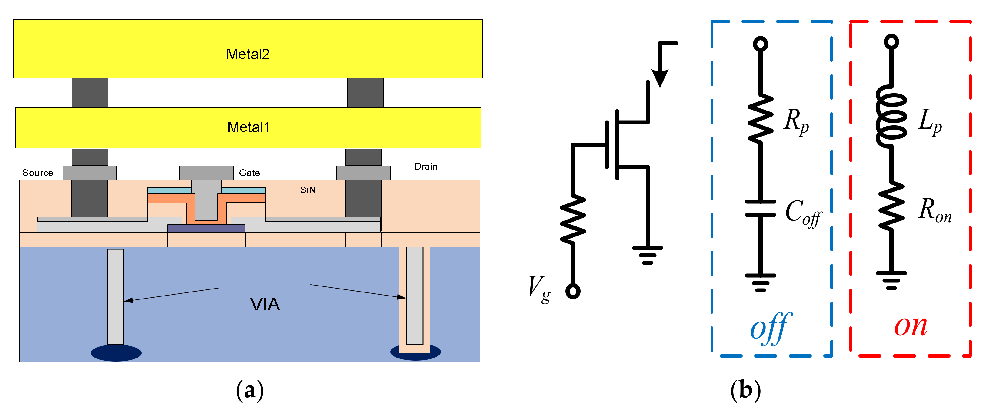
2.1. The 250 nm Phemt Technology

The proposed S32PT switch is fabricated on the 250 nm GaAs technology, as shown in Figure 2a. This process can implement a D/E-mode transistor by different implanting. Figure 2a illustrates a cross-section layer stack. The length of the gates is defined by the electron beam lithography. The process has two metal layers to realize the basic connections. The transmission lines and power lines in this design stack, MET1 and MET2, form into a thick metal layer with a high quality factor and low resistance.
The layers stacking is shown in Figure 2a. The different metal layers are connected by the vertical VIA. The wafer is passivized with a 200 nm-thick SiN layer, which acts as the dielectric layer of the metal–insulator–metal capacitors. After finishing the front-side process, a full back-side process follows, including the wafer thinning to a thickness of 50 μm, through substrate via holes and back-side metallization.

2.2. The Model of the Active Devices

The high-frequency modeling of the pHEMT is crucial for the switch design and the advantages of the accurate modeling are important [24,25,26,27,28]. The model of pHEMT as an equivalent circuit allows the device geometrical dimensions utilized to estimate the RF performances of the switches and theoretical analysis of the switch performance. The design specifications are related to the physical parameters of the device. With the proposed modeling and several design iterations, the optimum performances can be realized finally. To accurately predict and optimize the performance of the switch, the modeling of the GaAs has been developed in Figure 2. Compared to the transistors working in the amplifying state, the transistors work in the ON and OFF state for the switch. When the transistor works in the ON state, the transistor model is resistance and inductance in series, and the inductance is generated by the VIA, while the model in the process library does not consider the inductance of VIA. The C off of the transistor used in the proposed switch is 11–13 fF when the transistors work in the OFF state and the R on of the transistor used in the proposed switch is approximately 14.9 Ω when the transistors work in the ON state, and the cut-off frequency is 154 GHz. The control voltage for the gate is well above or below the threshold voltage.
When the gate voltage is set below the threshold, the transistor is utilized by the lumped elements, such as a capacitor with a resistor for representing the GaAs device under a “cold” condition, which considers the capacitive and resistive effects. When the gate voltage is well above the threshold, the GaAs device is completely in a “hot” condition, which mainly considers the resistive effects.

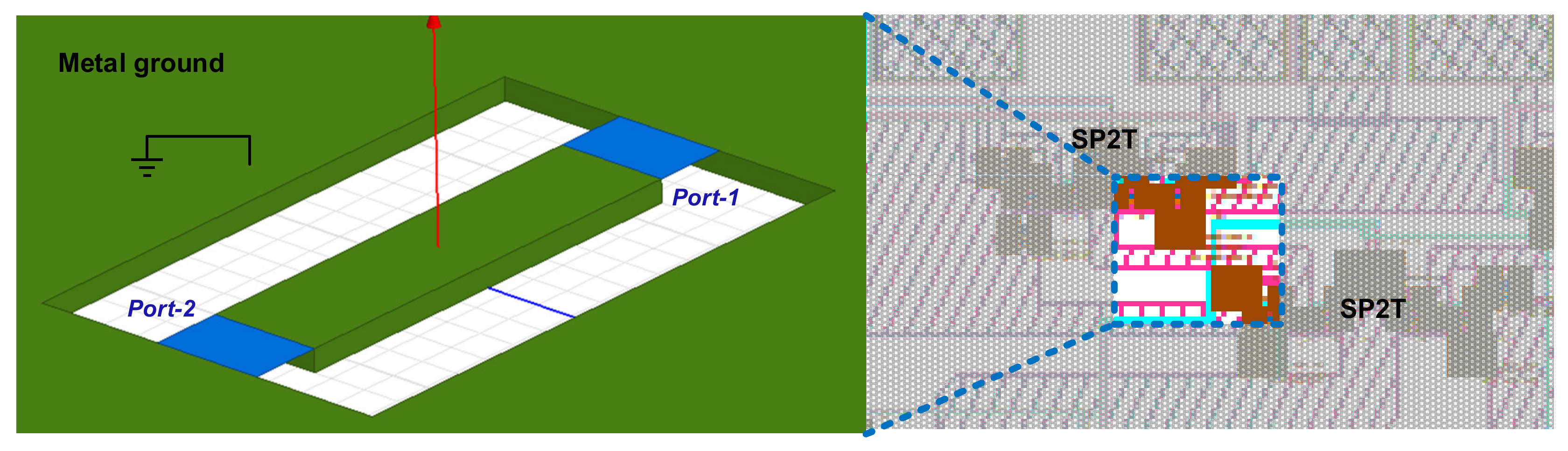
2.3. The EM Simulation of the Passive Device

Passive device modeling is important for the switch design due to the use of these devices for the input/output matching network and inter-stage matching. The manufactory provides some standard modeling of the capacitor, inductors and transmission lines. However, the model cannot meet the needs of customized passive components, such as inductors and transmission lines. The connection lines between the pHEMTs contribute to the inductance and capacitance, whose patterns are determined by the layout of the chip. Thus, it is essential to custom design and model the passive devices for optimum matching among the pHEMTs.
The full-wave 3D electromagnetic High-Frequency Structure Simulator (HFSS) was used to optimize the passive modeling process of the GaAs. The simulation steps are summarized as follows. Firstly, the physical layout layers of the semi-conductance were setup including the metal layers and isolation layer, such as the SiN layer based on the manufactory process, as shown in Figure 3. Secondly, the parameters of these layers are characterized by different parameters, such as thickness and conductance for metal layers and the loss tangent for isolation SiN layers. Thirdly, the reference ground for ports was defined and a custom design pattern was drawn in the HFSS. Finally, extracting the S parameter of the devices can be converted to Z/Y parameters for circuit design.

3. The Design Methodology for the SP32T Switch

This section shows the design methodology for the proposed SP32T switch that can be utilized for a highly parallelized and sub-6 GHz communications system.

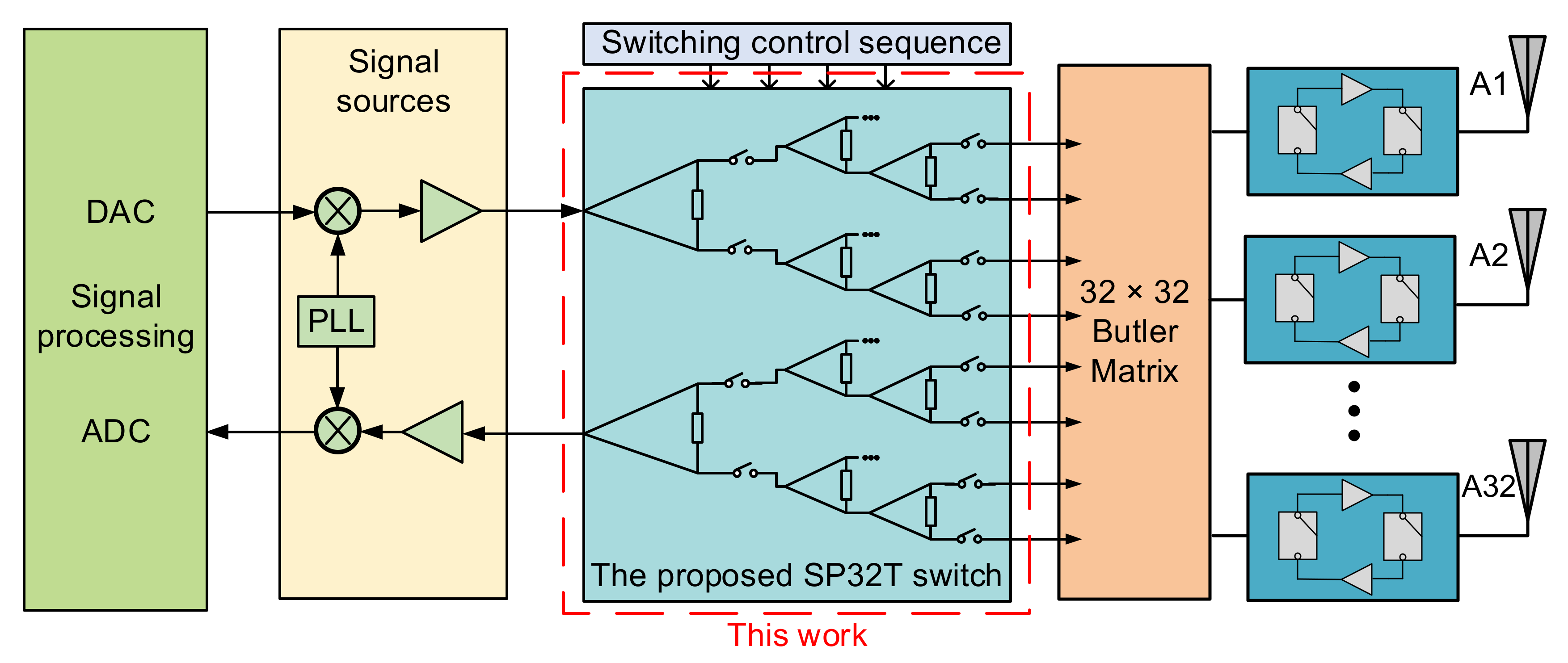
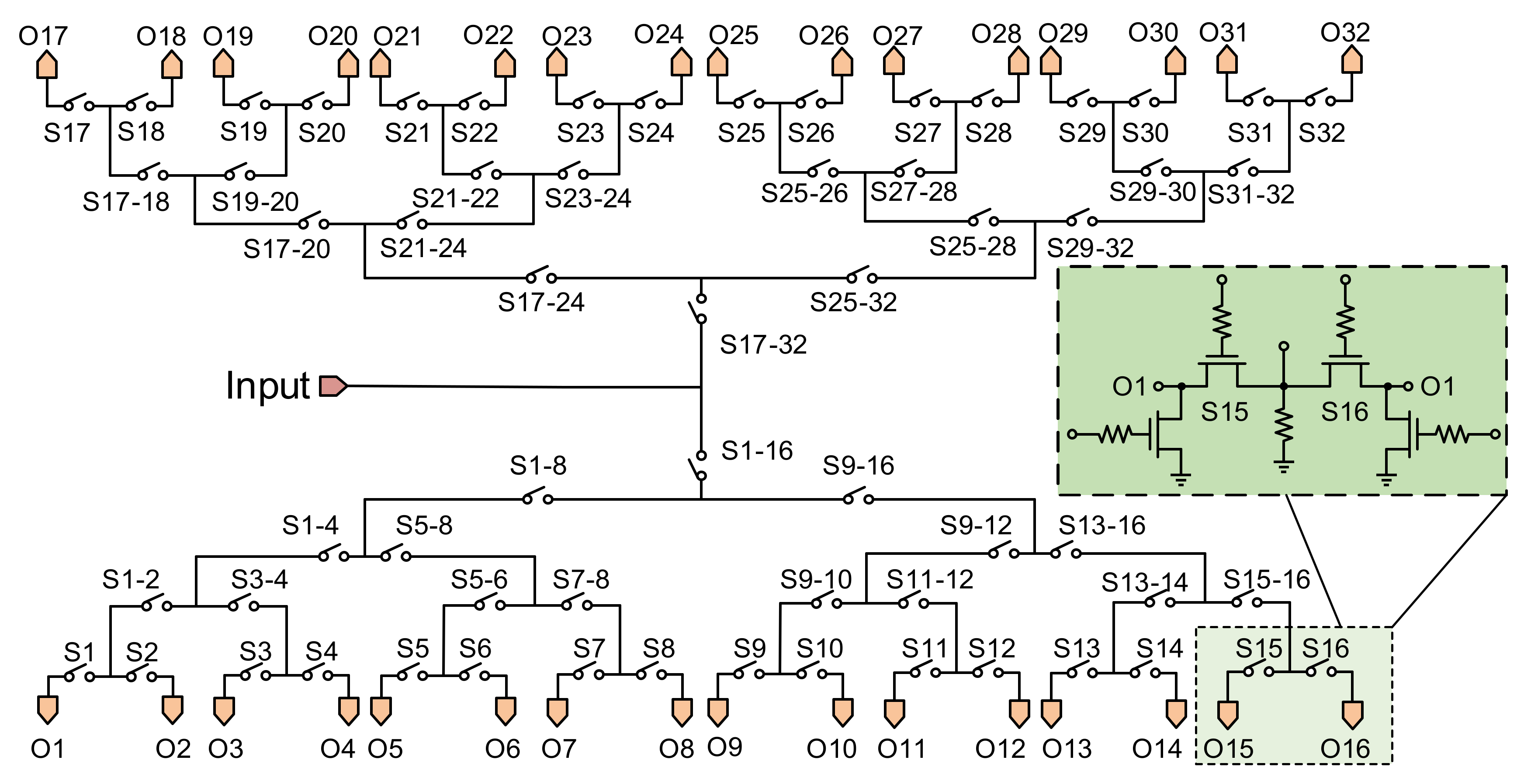
3.1. The System Design Requirement and Structure Analysis

Figure 4 describes the structure of the analog beamforming system which includes the SP32T switch. A heterodyne structure is selected with sub-6 GHz frequency. An intermediate frequency after down-mixing is around in the range of 10 MHz. The proposed communication system can share the same RF chains with the proposed switches. The total system power consumption is reduced to that of one chain without sacrificing the RF performance such as output power and noise figure of the transceiver. The strong variations in the RF amplification and time delays can significantly degrade the performance of the system. The other huge benefit of using the proposed structure is that the mismatches induced by the channels are eliminated due to one TRX channel utilized. As a result, these relaxed requirements for the system design help in optimizing the communication system to perform efficiently over a large bandwidth, minimizing the channel mismatches to improve the overall performance. The target applications for the sub-6 GHz SP32T T/R switch are 5G wireless communication and it is constructed by two asymmetric SP16T switches in a back-to-back connection, as shown in Figure 5.

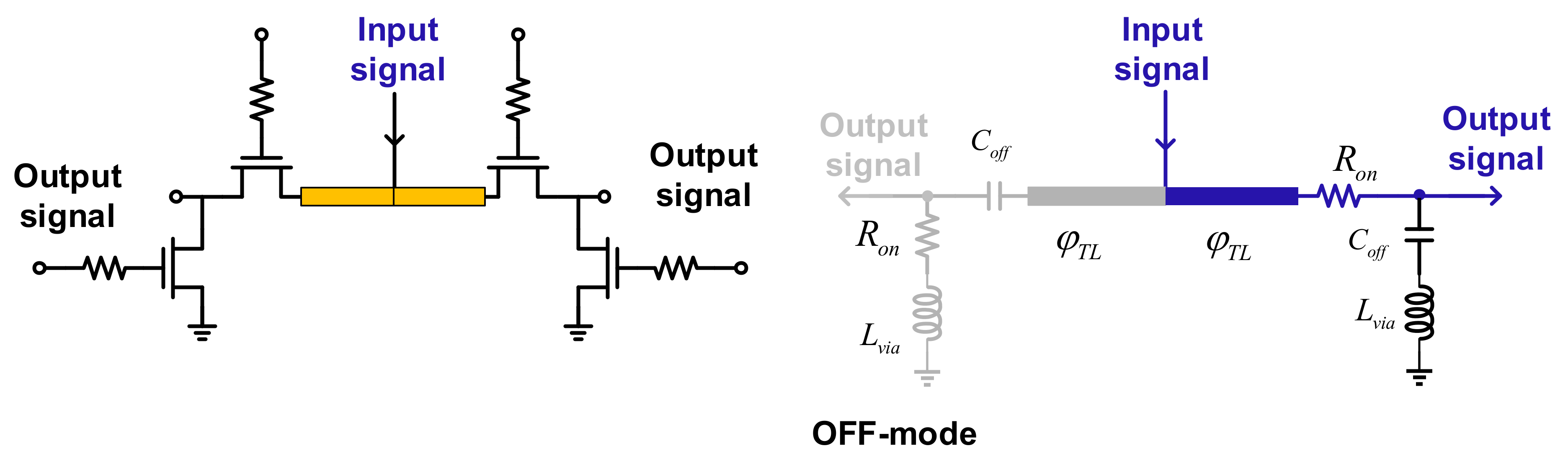
3.2. Transmission (ABCD) Matrix Design Methodology to Optimize the Insertion and Isolation Loss

The SP32T is composed of 16 SP2T and the 2 symmetric SPST switches. The common node of two SPST switches is denoted as Port 1, connecting to the output of the previous stage. The SP2T is a series-shunt structure, differing from the conventional structure which consists of two 50 ohm quarter-wavelength transmission lines. Consider that the impedance transformer is required to transform the low impedance of the OFF-state SPST switch to high impedance, and the IL of the ON-state SPST switch is large. The impedance transformer consumes a large area, leading to higher fabrication costs.
The series-shunt structure occupies small areas that are suitable for the multiple-output switches. To optimize the overall SP32T switch, the SP2T switch should be carefully designed. A design methodology is developed to optimize the insertion loss and return loss of the switch. The ON-state transistor is modeled as a resistance and the OFF-state transistor is modeled as a capacitor serial with an inductor induced by the VIA [29]. The transmission (ABCD) matrix can be expressed as:
A o n B o n C o n D o n = 1 R o n 0 1  
A o f f B o f f C o f f D o f f = 1 0 Y s 1 1  
Y s 1 = j ω C o f f 1 ω 2 L V I A C o f f  
where R o n is the resistor of the ON-state transistor, C o f f is the capacitor of the OFF-state transistor, and L V I A is the inductor of the VIA. The connection lines between the pHEMTs are modeled as transmission lines (TL) due to the high-frequency effect. The ABCD matrix of the transmission line is given as:
A T L B T L C T L D T L = c o s φ T L j Z 0 sin φ T L j Y 0 sin φ T L c o s φ T L
where Y 0   and   Z 0 are characteristic transconductance and impedance, respectively. φ T L is the electric length of the transmission line. Based on the ABCD matrix cascading features, the ABCD matrix of the ON-state switch can be expressed as:
A T B T C T D T = c o s φ T L j Z 0 sin φ T L j Y 0 sin φ T L c o s φ T L 1 R o n 0 1 1 0 Y s 1 1
where an element of the matrix can be written as:
A T = c o s φ T L j ω c R o n c o s φ T L + j Z 0 s i n φ T L ω 2 L v i a C o f f 1  
B T = R o n c o s φ T L + j Z 0 s i n φ T L
C T = j Y 0 s i n φ T L j ω c c o s φ T L + j R o n Y 0 s i n φ T L L v i a C o f f ω 2 1  
D T = c o s φ T L + j R o n Y 0 s i n φ T L
Based on Equations (6)–(9), F T can be derived as:
F T = A T + B T / Z 0 + C T Z 0 + D T = 2 c o s φ T L + R o n c o s φ T L + j Z 0 s i n φ T L Z 0 + j Y 0 s i n φ T L ( Z 0 + R o n )     j ω C o f f j Z 0 ( R o n Y 0 + 1 ) s i n φ T L + R o n + Z 0 c o s φ T L ω 2 L v i a C o f f 1
Referring to Equation (10), the insertion loss of the switch in the ON state can be calculated as:
I L 21 = 20 log S 21 = 20 log 2 F T
Equation (11) contains the resistance of the ON-state switch and the capacitor of the OFF-state switch. The electric length of the transmission line also affects its insert loss. By optimizing these parameters, insertion loss can be minimized.
In the OFF mode of the SP2T switch, the gate voltage of the transistor in the signal path is pulled down to low voltage, and the gate voltage of the shunt transistor is pulled up to high control voltage, synchronously. Therefore, the turn-OFF transistor is simply regarded as one OFF-state capacitance serving as a part of the matching network and the turn-ON transistor exhibits a small resistance. Figure 6 shows the small-signal equivalent circuit for the SPDT in the OFF mode. The ABCD matrix between Port 1 and Port 2 can be represented as:
A T O B T O C T O D T O = c o s φ T L j Z 0 sin φ T L j Y 0 s i n φ T L c o s φ T L 1 1 / j ω C o f f 0 1 1 0 Y s 2 1
Y s 2 = 1 R o n + j ω L v i a  
where the element of the matrix can be given as
A T O = c o s φ T L + R o n c o s φ T L + j Z 0 s i n φ T L R o n + j ω L v i a  
B T O = R o n c o s φ T L + j Z 0 s i n φ T L
C T O = j Y 0 s i n φ T L + c o s φ T L + j R o n Y 0 s i n φ T L R o n + j ω L v i a
C T O = c o s φ T L + j R o n Y 0 s i n φ T L
Considering Equations (14)–(17), F T O can be written as:
F T O = A T O + B T O / Z 0 + C T O Z 0 + C T O = 2 c o s φ T L + j Y 0 s i n φ T L Z 0 + R o n + c o s φ T L Z 0 + R o n + ( R o n Y 0 + 1 ) s i n φ T L j Z 0 R o n + j ω L v i a             + R o n c o s φ T L + j Z 0 s i n φ T L Z 0
Hence, the isolation of the switch in the OFF state can be derived as:
ISO 21 = 20 log S 21 = 20 log 2 F T O
This equation contains the resistance of the ON-state switch and the capacitor of the OFF-state switch. The electric length of the transmission line affects the loss and matching. the isolation can be maximized by optimizing these parameters.

3.3. Transmission (ABCD) Matrix Optimization for the SP32T Switch

Key specifications of the SP2T switch have been conducted and optimized by the ABCD matrix for both the ON/OFF states. With the same design methodology, the total insertion loss and isolation of SP32T can be summarized as:
I L I L n = A B C D T 1 A B C D T 2 A B C D T 3 A B C D T 4
I L I S O n = A B C D T 1 A B C D T 2 A B C D T 3 A B C D I S O 4
where the subscript T 1 , 2 , 3 , 4   of the matrix represents the stages of the SP2T switches in the ON state, and subscript I S O 1 , 2 , 3 , 4 of the matrix represents the stages of the SP2T switches in the OFF state.
Based on Equations (20) and (21) for the insertion and isolation of SP32T, the optimizing design follows was summarized as follows. Firstly, extract the ON-state resistance and OFF-state capacitance of the pHEMT with the serial inductance of the VIA. Secondly, determine the total width of the pHEMT based on the equation according to the required insertion loss and isolation. Thirdly, optimizing the inter-stage matching based on the total insertion loss and isolation, based on the above process with several time design iterations. The size is shown in Figure 7 with the passive element values of the proposed SPDT switch optimized eventually from the post-layout simulations with ADS. The calculated and optimized active device dimensions are quite close to each other. The calculated values of the passive elements are larger than the optimized values, mainly due to the parasitic capacitor of the layout is not included in the calculation.

3.4. ESD Protection and Switch Speed Design for Control Signals

In this paper, on-chip electrostatic discharge protection (ESD) is implemented to make the chip robust during the application. The basic working principle of ESD is to provide discharging loop when the input signal voltage is a sharp voltage pulse within a short time. On-chip pads of the switch are classified into microwave-frequency pads and low-frequency pads. Since the microwave-frequency pads are more sensitive to the parasitic capacitor of the extra-protection circuit. These pads are connected to the drains of the pHEMTs, and the diodes of the drain can be used to realize the ESD protection.
Compared with the pads connected to the drains of the pHEMTs, the gate is more fragile due to its high impedance and no discharge loop [30]. The ESD protection of the switch is for control pads. Referring to the system requirement, the turn-ON/OFF speed of the switch determines the imaging speed. A large ESD protection circuit will induce large parasitic capacitance to the control pads. Thus, there is a trade-off between ESD protection and switching speed.
The two design steps for the ESD protection are listed as follows. The current protection ability of the ESD was simulated to resize the diode and predict the ESD performance [31,32]. Based on the simulation results, a geometry of diode can be selected, resulting in minimum performance degradation of the ESD-induced circuit. An anti-parallel diode-string ESD protection circuit is chosen in this design. Different ESD device sizes can be stressed by an ESD transient voltage or current generated by the equivalent ESD discharging circuit HBM ESD model for a targeted ESD protection level, as shown in Figure 8. Secondly, the speed of the switch is highly related to the capacitor of the gate. The control voltages must charge and discharge the capacitor to a certain voltage to turn on and off the transistor. The parasitic capacitor on the gate forms a low pass filter characteristic that degrades the high-frequency performance. The turn-ON/OFF speed is a 50 ns requirement for this switch and the total capacitor value of the gate can be determined.
Hence, the co-design of the ESD protection and the switch circuit is essential to optimize both the ESD protection and the operating speed of the switch. The ESD current and voltage simulation were carefully conducted to predict the ESD capability and high-speed switching needed to minimize the parasitic capacitor. After several design iterations, the ESD diode is optimized as an eight-finger diode with a width of 60 μm and the switch speed is 100 MHz.

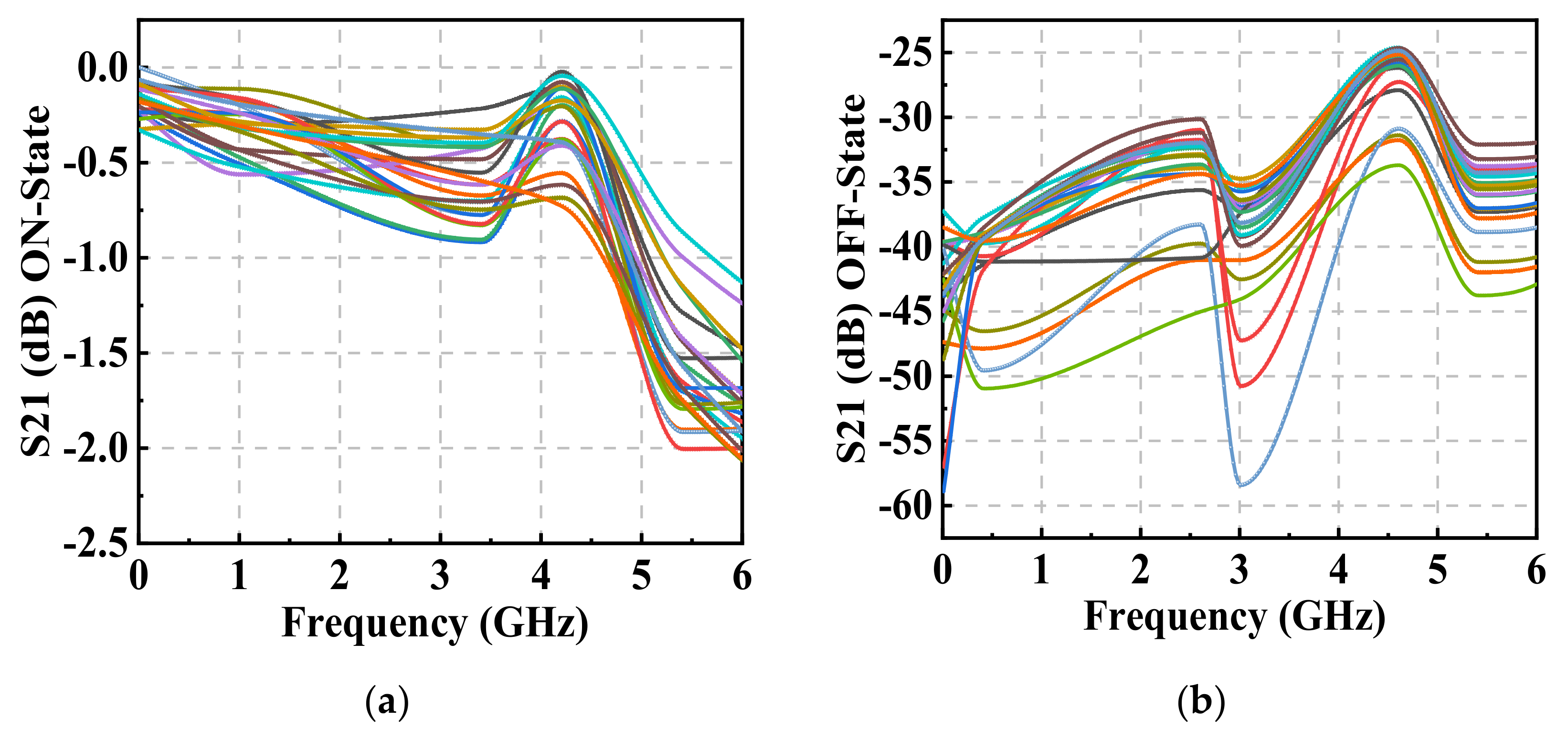
4. Measurement Results

In this section, the specifications of the single-chip switch were assessed. To reduce the RF power reflections between the amplifiers and switches and avoid the unwanted coupling effects, the input and output impedance-matching networks for the switches are important, and the return loss is set to <10 dB over the 6 GHz frequency range of interest.

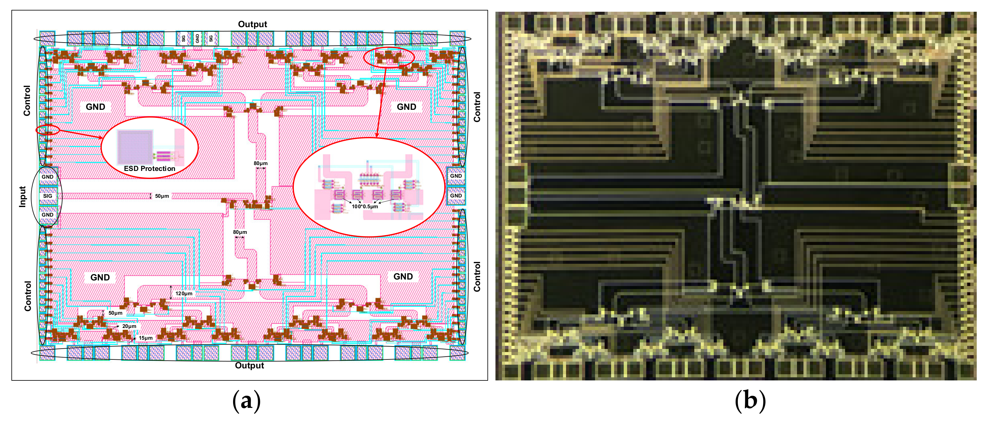
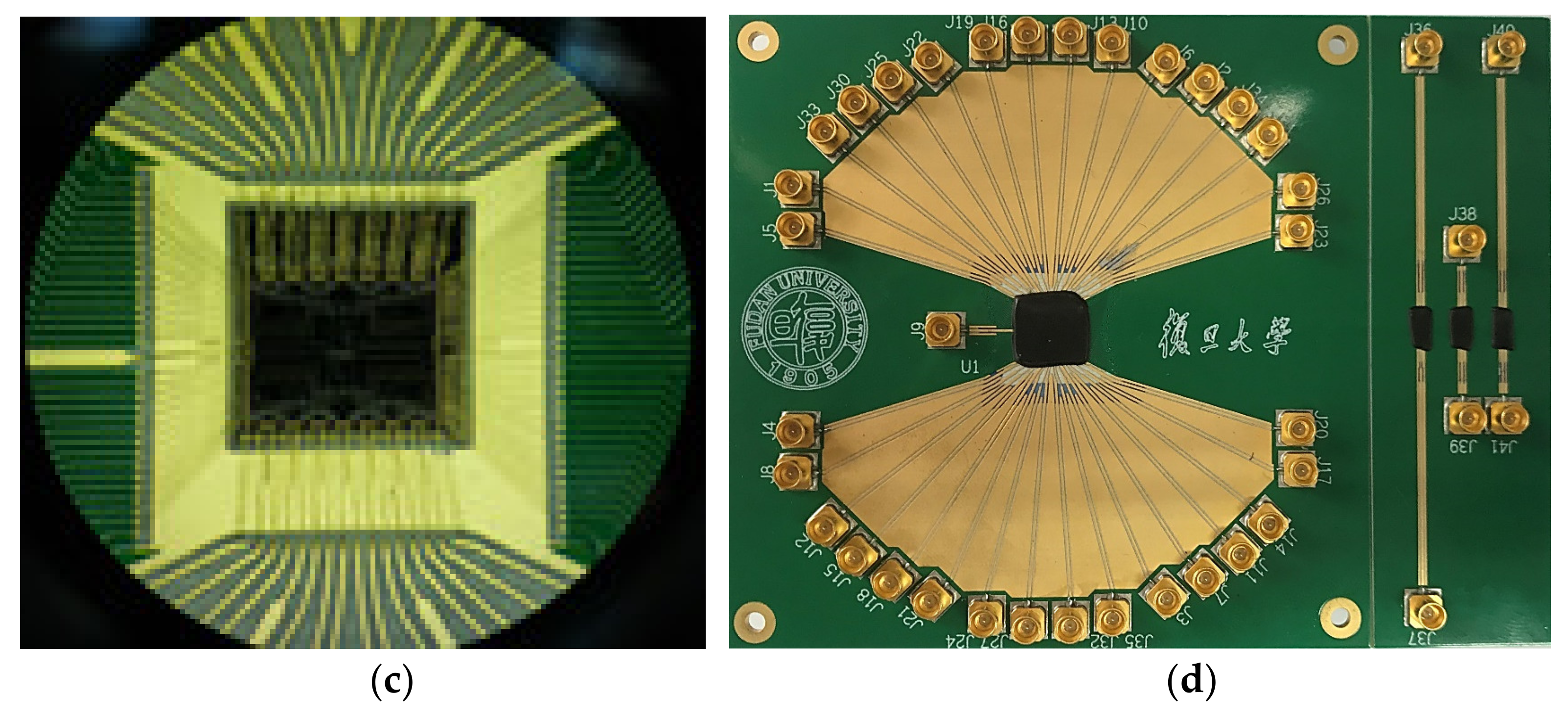
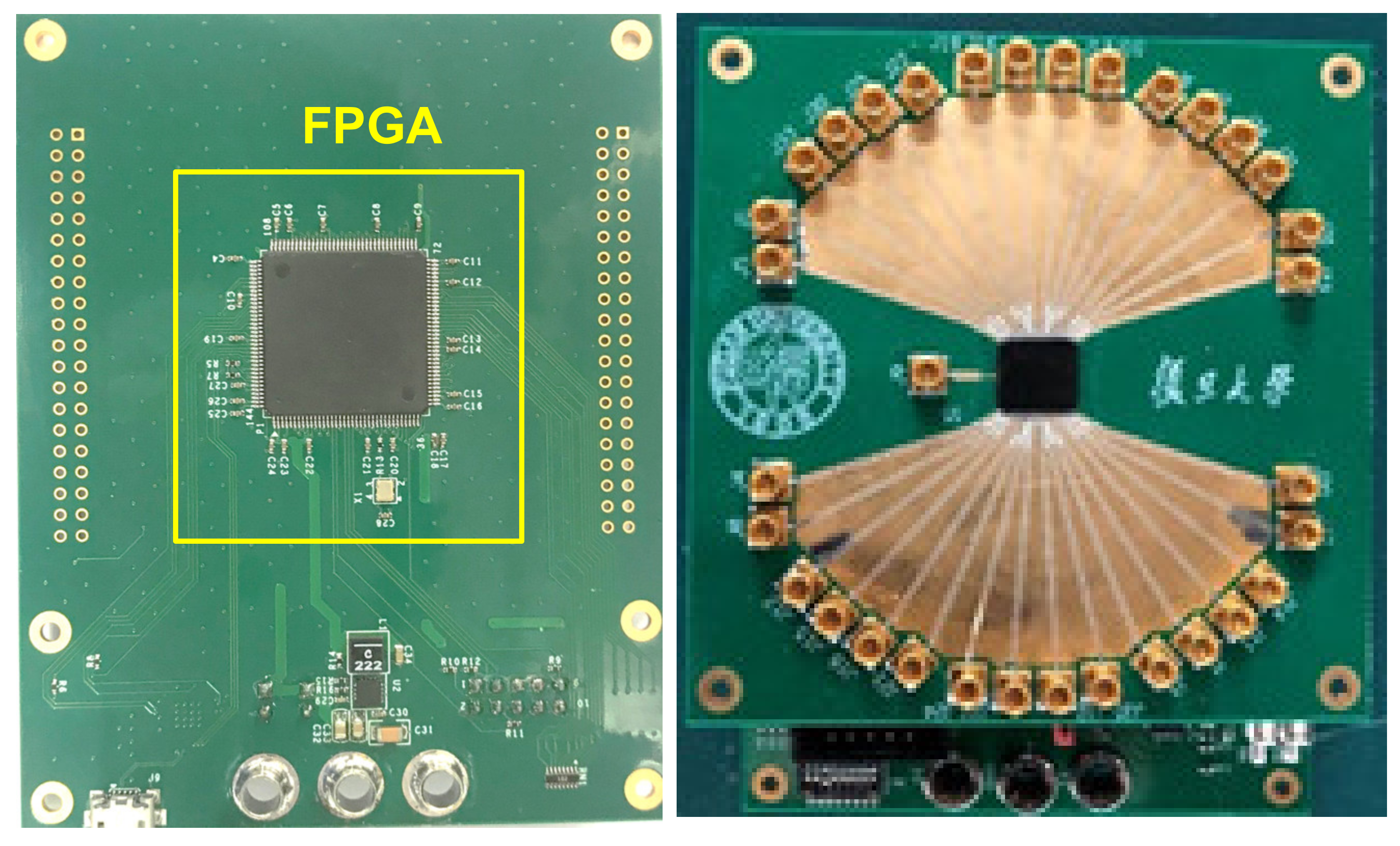
4.1. Chip and Package Design for Testing

The proposed SP32T switch was fabricated in a GaAs process for a sub-6 GHz communications system. It achieves a working frequency of up to 6 GHz. Figure 9 shows that the whole chip area including all testing pads is 12 mm2 and also shows the printed circuit board (PCB).
Interconnections between the chip and PCB are a key consideration for the package operating at the mm-wave band. In this design, the wire-bonding method is utilized for the chips and PCB connection. The bonding wires perform as an ideal wire connection at low frequencies. However, as the frequency increases, the model of the wire bonds is inductors. To accurately model these inductors, the wire bonds were simulated by the HFSS tool. The switch is bonded to the chip on board (COB) in a cavity for the shortest bonding wires. The bandwidth of the wire bonds is optimized to matching the pad capacitance to 50 ohm transmission lines on PCB.

4.2. Chip and Package Design for Testing

To accurately assess the performance of our chip, a dedicated calibration pattern is designed. The calibration patterns are conducted by including the bonding wires, transmission lines and connectors. These parasitic effects were de-embedded because the same bonding wire structures utilized in the design were fabricated and measured. With several different testing patterns, as shown in Figure 10, the loss of the transmission line, connectors and the bonding wire can be predicted precisely.
Agilent E3631A DC voltage source was used as power supply equipment, and Keysight N5247B vector network analyzer was used to measure the S parameter. The measured input/output return losses are illustrated in Figure 11. The measured input is better than 10 dB from 1 GHz to 6 GHz. The output return loss is also maintaining < −10 dB from 1 GHz to 6 GHz. The measured results are worse than the simulation. The measured return losses verify the proposed SP32T switch topology that can successfully solve the issue of the impedance mismatching induced by the bonding wire.
As shown in Figure 12a, the measured average insertion loss (IL) is 1 dB over the bandwidth of 0–6 GHz. Additionally, the measured isolations between ports are plotted in Figure 12b. The switch achieves the measured average isolation of 35 dB at 5 GHz. There are discrepancies between the simulated and measured performances, which are dominantly due to the inaccuracy of the transistor models. The proposed SP32T switch consumes a much smaller die area and achieves competitive performance.

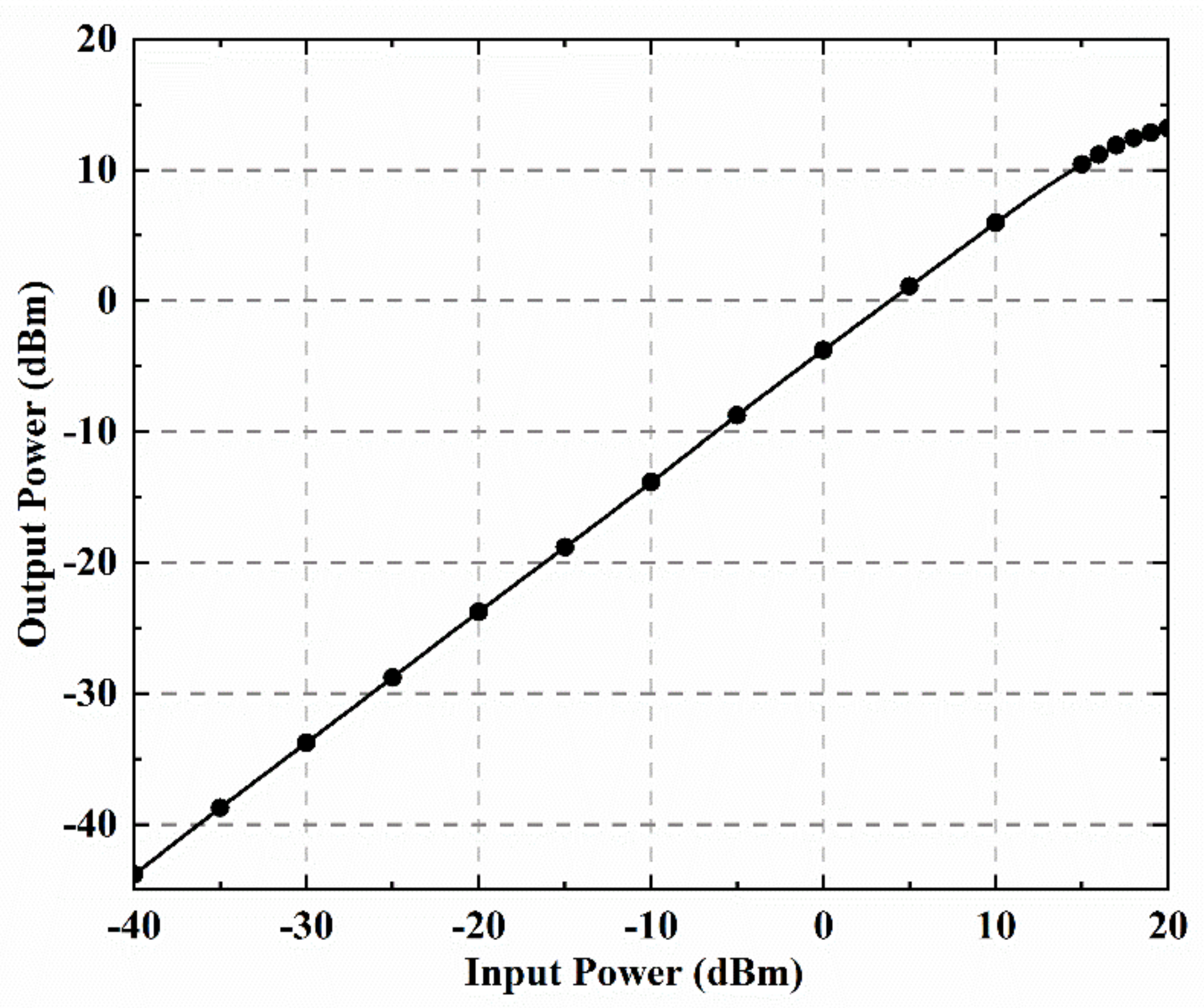
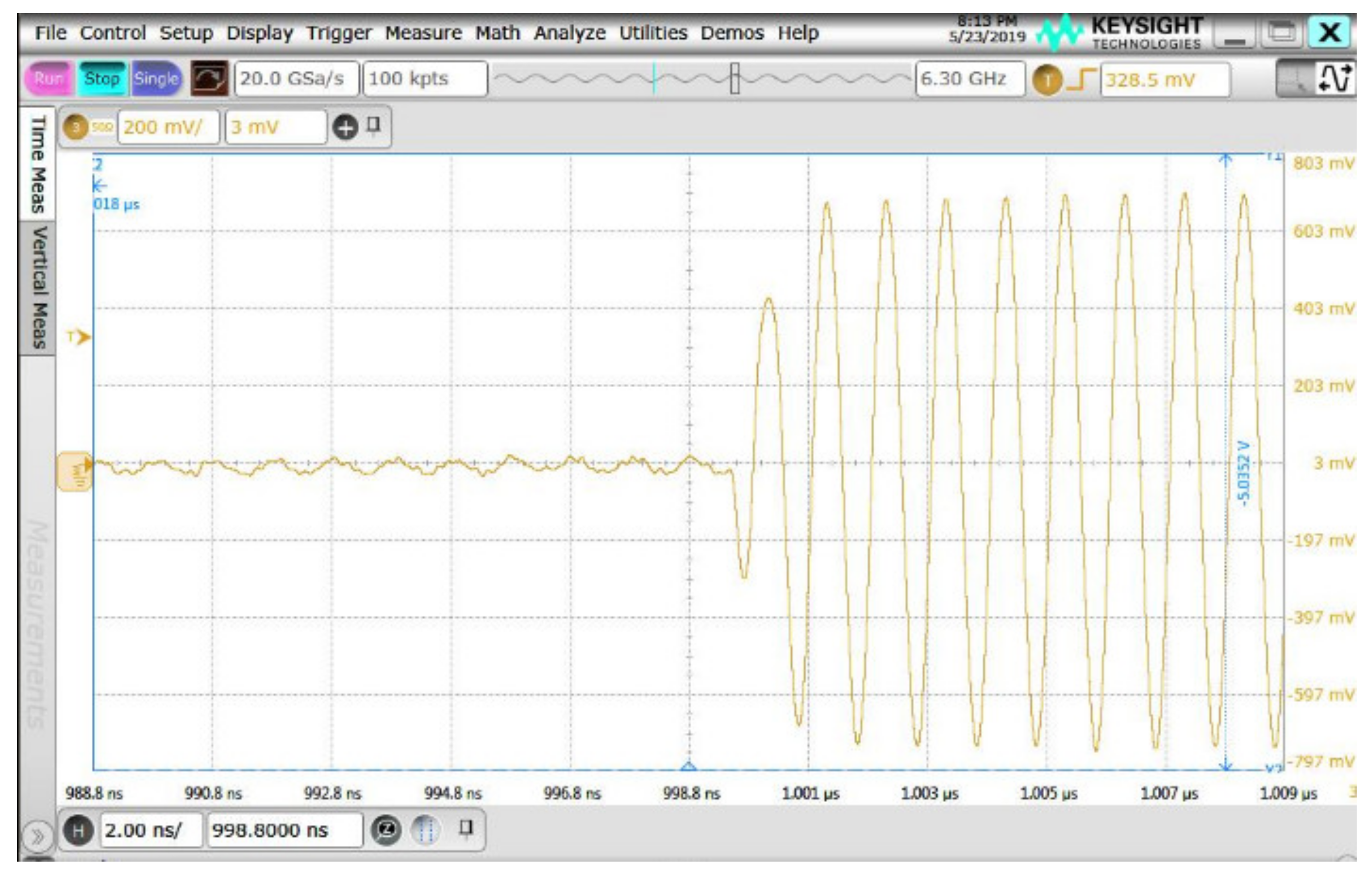
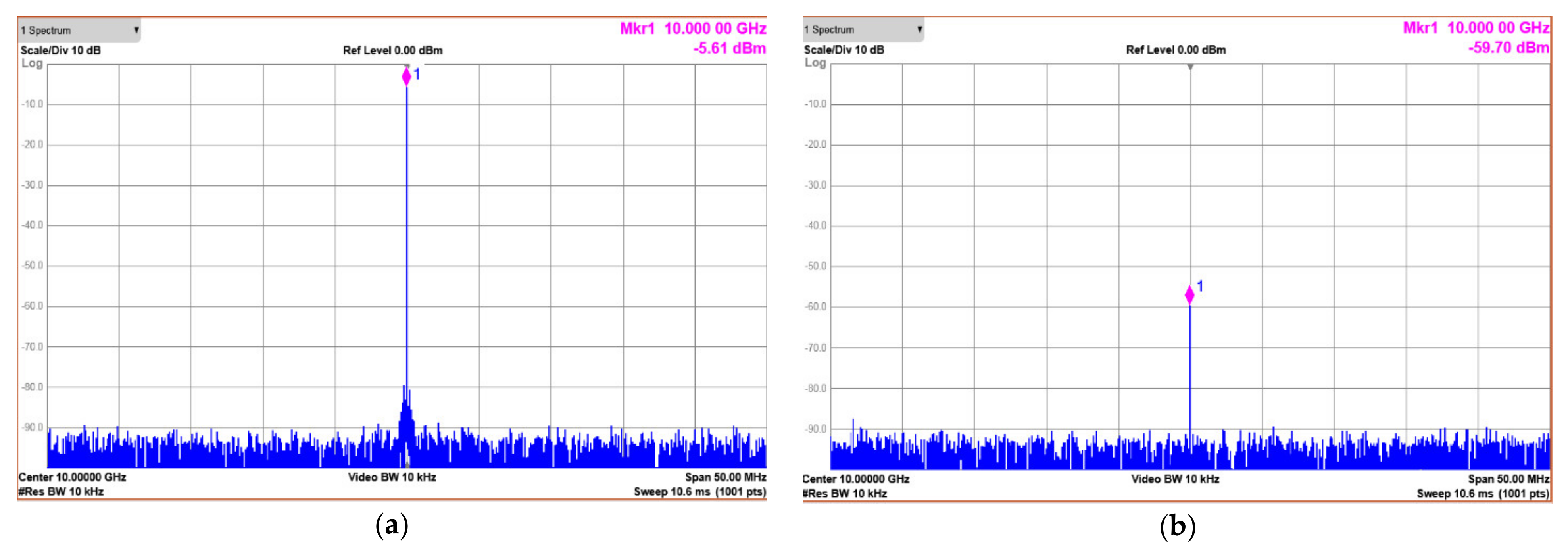
4.3. Linearity and Switching Speed Measurement

The linearity of the switch is characterized by the input power compressed by 1 dB (P1dB). Different input powers were utilized to measure the P1dB, which is approximately 15 dBm, as shown in Figure 13. The input of the single-chip switch is connected to the signal generator (E8257D Keysight) with a frequency of up to 67 GHz and its output is connected to the signal analyzer (N9040B Keysight) with a measurement frequency of up to 50 GHz.
To assess the operating speed of the switch, different input frequencies and switching control signals are performed. Agilent 33250A function/arbitrary waveform generator was used to generate the control signals. Additionally, Keysight E8257D signal generator was used to generate the different input frequencies. The transient measurement switching speed of the proposed SP32T is shown in Figure 14, Figure 15 and Figure 16, when inputting the 10 MHz gate control signal waveform. The period of ON/OFF time for the switch is 50 ns. The transient time transferring from the turn-ON to turn-OFF is very fast at 1 ns, including a coaxial cable propagation delay of 0.5 ns. The measurement results show the proposed switch has ultra-fast speed and is feasible for the sub-6 GHz communications system. Additionally, the spectrum measurements are also utilized to check the isolation when the switch is turn-ON and turn-OFF, as shown in Figure 17. Compared with the switches in Table 1, the proposed chip can achieve low loss with 32 outputs. In the future, the chip area of the proposed switch can be reduced by optimizing the channel layout and transmission line structure.

5. Conclusions

This paper reports a highly integrated SP32T switch fabricated in a 0.25 μm GaAs process. The proposed SP32T single-chip switch consumes ultra-low power and occupies a smaller core area of 12 mm2 including all the testing pads. Additionally, this paper proposes a design methodology for optimizing our SP32T switch and shows good agreement with the measured results. Thus, the switch design methodology facilitates the design of the mm-wave switches and can be applied to other semiconductor technologies and switch topologies. Compared to the SP32T switch that is implemented by the waveguide module, the proposed switch shows low-power consumption, high integration, and better consistency between different channels. The measured performance at 6 GHz exhibits an average IL of 1.5 dB, an average isolation of 35 dB, an input/output return losses better than 10 dB, and a switch speed of 50 ns, respectively.

Author Contributions

Research methodology, T.W., S.M. and J.W.; writing—original draft preparation, T.W., S.M.; supervision, J.R.; validation, T.W., S.M., J.W. and H.L.; writing—review and editing, S.M., Y.C. and T.W. All authors have read and agreed to the published version of the manuscript.

Funding

This work was supported by the National Natural Science Foundation of China under Grant 61934008 and Natural Science Foundation of Shanghai (Grant No. 21ZR1405700).

Data Availability Statement

Data is contained within the article. The data presented in this study are available in this paper.

Conflicts of Interest

The authors declare no conflict of interest.

References

  1. Larsson, E.G.; Edfors, O.; Tufvesson, F.; Marzetta, T.L. Massive MIMO for next generation wireless systems. IEEE Commun. Mag. 2014, 52, 186–195. [Google Scholar] [CrossRef] [Green Version]
  2. Gupta, A.; Jha, R.K. A survey of 5G network: Architecture and emerging technologies. IEEE Access 2015, 3, 1206–1232. [Google Scholar] [CrossRef]
  3. Yu, H.; Chen, Y.; Boon, C.; Mak, P.; Martins, R. A 0.096-mm2 1-20-GHz triple-path noise-canceling common-gate common-source LNA with dual complementary pMOS-nMOS configuration. IEEE Trans. Microw. Theory Technol. 2020, 68, 144–159. [Google Scholar] [CrossRef]
  4. Yu, H.; Chen, Y.; Boon, C.C.; Li, C.; Mak, P.-I.; Martins, R.P. A 0.044-mm2 0.5-to-7-GHz resistor-plus-source-follower-Feedback noise-cancelling LNA achieving a flat NF of 3.3 ± 0.45 dB. IEEE Trans. Circ. Syst. II Exp. Briefs 2019, 66, 71–75. [Google Scholar] [CrossRef]
  5. Djerafi, T.; Fonseca, N.J.G.; Wu, K. Planar Ku-band 4 × 4 Nolen matrix in SIW technology. IEEE Trans. Microw. Theory Technol. 2010, 58, 259–266. [Google Scholar] [CrossRef]
  6. Cetinoneri, B.; Atesal, Y.A.; Rebeiz, G.M. An 8 × 8 Butler matrix in 0.13 μm CMOS for 5-6-GHz multibeam applications. IEEE Trans. Microw. Theory Technol. 2011, 59, 295–301. [Google Scholar] [CrossRef]
  7. Bona, M.; Manholm, L.; Starski, J.P.; Svensson, B. Low-loss compact Butler Matrix for a microstrip antenna. IEEE Trans. Microw. Theory Technol. 2020, 50, 2069–2075. [Google Scholar] [CrossRef]
  8. Vahabisani, N.; Daneshmand, M. Monolithic millimeter-wave MEMS waveguide switch. IEEE Trans. Microw. Theory Technol. 2015, 63, 340–351. [Google Scholar] [CrossRef]
  9. Lin, Y.-C.; Yen, S.; Mukherjee, T.; Fedder, G.K. Lateral Flexure Contact on CMOS MEMS Electrothermal Metal-Metal Contact Switch by Platinum ALD Sidewall Patterning. In Proceedings of the IEEE International Conference on Micro Electro Mechanical Systems (MEMS), Gainesville, FL, USA, 25–29 January 2021; pp. 974–977. [Google Scholar]
  10. Vahabisani, N.; Daneshmand, M. Realization of a new class of monolithic RF MEMS waveguide switches for millimeter-wave applications. In Proceedings of the IEEE MTT-S International Microwave Symposium, Tampa, FL, USA, 1–6 June 2014; pp. 1–4. [Google Scholar]
  11. Daneshmand, M.; Fouladi, S.; Mansour, R.R.; Lisi, M.; Stajcer, T. Thermally actuated latching RF MEMS switch and its characteristics. IEEE Trans. Microw. Theory Technol. 2009, 57, 3229–3238. [Google Scholar] [CrossRef]
  12. Fedder, G.K.; Howe, R.T.; Liu, T.-J.K.; Quevy, E.P. Technologies for cofabricating MEMS and electronics. Proc. IEEE 2008, 96, 306–322. [Google Scholar] [CrossRef]
  13. Lin, Y.C.; Chung, V.P.J.; Santhanam, S.; Mukherjee, T.; Fedder, G.K. Sidewall metallization on CMOS MEMS by platinum ALD patterning. J. Microelectromech. Syst. 2020, 29, 978–983. [Google Scholar] [CrossRef]
  14. Analog Devices, ADGM1004 Datasheet, Analog Devices. Norwood, MA, USA. 2020. Available online: https://www.analog.com/media/en/technical-documentation/data-sheets/adgm1004.pdf (accessed on 15 June 2021).
  15. Menlo Micro, MM5120 Product Berief, Menlo Micro. Irvine, CA, USA. 2020. Available online: https://menlomicro.com/images/general/MM5120_Product_Brief.pdf (accessed on 15 June 2021).
  16. Singh, T.; Mansour, R.R. Chalcogenide phase change material GeTe based inline RF SPST series and shunt switches. In Proceedings of the IEEE MTT-S International Microwave Workshop Series on Advanced Materials and Processes for RF and THz Applications (IMWS-AMP), Ann Arbor, MI, USA, 16–18 July 2018; pp. 1–3. [Google Scholar]
  17. Crunteanu, A.; Mennai, A.; Guines, C.; Passerieux, D.; Blondy, P. Out-of-plane and inline RF switches based on Ge2Sb2Te5 phase-change material. In Proceedings of the IEEE MTT-S International Microwave Symposium, Tampa, FL, USA, 1–6 June 2014; pp. 1–4. [Google Scholar]
  18. Hariri, A.; Crunteanu, A.; Guines, C.; Hallepee, C.; Passerieux, D.; Blondy, P. Double-port double-throw (DPDT) switch matrix based on phase change material (PCM). In Proceedings of the 48th European Microwave Conference (EuMC), Madrid, Spain, 23–27 September 2018; pp. 479–482. [Google Scholar]
  19. Bettoumi, I.; Guines, C.; Blondy, P. A Dynamic CAD Model for Phase Change Material (PCM) Switches. In Proceedings of the 50th European Microwave Conference (EuMC), Utrecht, The Netherlands, 12–14 January 2021; pp. 658–661. [Google Scholar]
  20. Singh, T.; Mansour, R.R. Investigation into self actuation limitation and current carrying capacity of chalcogenide phase change GeTe-based RF switches. IEEE Trans. Electron Devices 2020, 67, 5717–5722. [Google Scholar] [CrossRef]
  21. Singh, T.; Mansour, R.R. Characterization, optimization, and fabrication of phase change material germanium telluride based miniaturized DC–67 GHz RF switches. IEEE Trans. Microw. Theory Technol. 2019, 67, 3237–3250. [Google Scholar] [CrossRef]
  22. Yamamoto, K.; Moriwaki, T.; Fujii, T.; Otsuji, J.; Miyashita, M.; Miyazaki, Y.; Nishitani, K. A 2.2-V Operation, 2.4-GHz Single-Chip GaAs MMIC Transceiver for Wireless Applications. IEEE J. Solid State Circ. 1999, 34, 502–512. [Google Scholar] [CrossRef]
  23. Chao, S.-F.; Kuo, C.-C.; Tsai, Z.-M.; Lin, K.-Y.; Wang, H. 40-GHz MMIC SPDT and Multiple-Port Bandpass Filter-Integrated Switches. IEEE Trans. Microw. Theory Technol. 2007, 55, 2691–2699. [Google Scholar] [CrossRef]
  24. Snowden, C.M. Large-Signal Microwave Characterization of AlGaAs/GaAs HBT’s Based on a Physics-Based Electrothermal Model. IEEE Trans. Microw. Theory Technol. 1997, 45, 58–71. [Google Scholar] [CrossRef] [Green Version]
  25. Cidronali, A.; Collodi, G.; Santarelli, A.; Vannini, G.; Manes, G. Millimeter-Wave FET Modeling Using On-Wafer Measurements and EM Simulation. IEEE Trans. Microw. Theory Technol. 2002, 50, 425–432. [Google Scholar] [CrossRef]
  26. Liou, L.L.; Ebel, J.L.; Huang, C.I. Thermal Effects on the Characteristics of AlGaAs/GaAs Heterojunction Bipolar Transistors Using Two-Dimensional Numerical Simulation. IEEE Trans. Electron Device 1993, 40, 35–43. [Google Scholar] [CrossRef]
  27. Frankel, M.Y.; Pavlidis, D. An Analysis of the Large-Signal Characteristics of AlGaAs/GaAs Heterojunction Bipolar Transistors. IEEE Trans. Microw. Theory Technol. 1992, 40, 465–474. [Google Scholar] [CrossRef]
  28. Crupi, G.; Xiao, D.; Schreurs, D.P.; Limiti, E.; Caddemi, A.; De Raedt, W.; Germain, M. Accurate Multibias Equivalent-Circuit Extraction for GaN HEMTs. IEEE Trans. Microw. Theory Technol. 2006, 54, 3616–3622. [Google Scholar] [CrossRef]
  29. Mizutani, H.; Ishikawa, R.; Honjo, K. InGaAs MMIC SPST Switch Based on HPF/LPF Switching Concept with Periodic Structure. IEEE Trans. Microw. Theory Technol. 2016, 64, 2863–2870. [Google Scholar] [CrossRef]
  30. Wang, X.S.; Wang, X.; Lu, F.; Zhang, C.; Dong, Z.; Wang, L.; Ma, R.; Shi, Z.; Wang, A.; Chang, M.C.F.; et al. Concurrent Design Analysis of High-Linearity SP10T Switch With 8.5 kV ESD Protection. IEEE J. Solid State Circ. 2014, 49, 1927–1941. [Google Scholar] [CrossRef]
  31. Wang, A.Z.; Feng, H.; Zhan, R.; Xie, H.; Chen, G.; Wu, Q.; Guan, X.; Wang, Z.; Zhang, C. A Review on RF ESD Protection Design. IEEE Trans. Electron Device 2005, 52, 1304–1311. [Google Scholar] [CrossRef]
  32. Wang, L.; Ma, R.; Wang, A.; Wang, X.; Zhao, B.; Wang, S.X.; Yue, P.; Shi, Z.; Cheng, Y. A Design Technique Overview on Broadband RF ESD Protection Circuit Designs. In Proceedings of the Proc. IEEE International Midwest Symposium on Circuits and Systems (MWSCAS), Boise, ID, USA, 5–8 August 2012; pp. 590–593. [Google Scholar]
  33. Chipengo, U.; Commens, M. A 77 GHz simulation study of roadway infrastructure radar signatures for smart roads. In Proceedings of the 16th European Radar Conference (EuRAD), Paris, France, 2–4 October 2019; pp. 137–140. [Google Scholar]
  34. Sari, S.; Tulasi Sivakumar, D.; Nagaveni, H.; Karthik, S. DC-6 GHz GaAs MMIC Compact SPDT Switch. In Proceedings of the 2020 IEEE International Conference for Innovation in Technology (INOCON), Bangluru, India, 6–8 November 2020; pp. 1–4. [Google Scholar]
  35. Tuthill, M. A Switched-Current, Switched-Capacitor Temperature Sensor in 0.6 μm CMOS. IEEE J. Solid State Circ. 1998, 33, 1117–1122. [Google Scholar] [CrossRef]
  36. Li, Q.; Zhang, Y.P. CMOS T/R Switch Design: Towards Ultra-Wideband and Higher Frequency. IEEE J. Solid State Circ. 2007, 42, 563–570. [Google Scholar] [CrossRef]
  37. Han, Y.; Carter, K.; Larson, L.; Behzad, A. A low insertion loss, high linearity, T/R switch in 65 nm bulk CMOS for WLAN 802.11g applications. In Proceedings of the IEEE Radio Frequency Integrated Circuits Symposium, Atlanta, GA, USA, 15–17 June 2008; pp. 681–684. [Google Scholar]
Figure 1. Structure block diagram of a single-pole multi-throw (SPMT) switch used in an analog beamforming system with a Butler matrix.
Electronics 10 01482 g001
Figure 2. (a) The cross-section of the GaAs process; (b) the model of the transistor in different states.
Electronics 10 01482 g002
Figure 3. The simulation setup for the transmission line utilized in this switch.
Electronics 10 01482 g003
Figure 4. The sub-6 GHz 5G communication system structure using the proposed SP32T switches. DAC: digital-to-analog converter; ADC: analog-to-digital converter.
Electronics 10 01482 g004
Figure 5. The proposed tree structure for the SP32T with high isolation between different channels.
Electronics 10 01482 g005
Figure 6. The switch with transmission line connection and different mode analysis.
Electronics 10 01482 g006
Figure 7. The details of the signal path from input to output when activating one channel.
Electronics 10 01482 g007
Figure 8. The simulation results of the electrostatic discharge (ESD) protection and the proposed SP2T switch.
Electronics 10 01482 g008
Figure 9. The details of the proposed single-chip switch: (a) layout; (b) chip photo; (c) bonding package; (d) chip on board (COB).
Electronics 10 01482 g009aElectronics 10 01482 g009b
Figure 10. The timing control board and control logic for the COB.
Electronics 10 01482 g010
Figure 11. The matching in different channels for the input and output for the COB with bonding wires.
Electronics 10 01482 g011
Figure 12. (a) The insertion loss of the switch in different channels; (b) The isolation of the switch in different channels. There is a variation due to bonding wire mismatch.
Electronics 10 01482 g012
Figure 13. The P1dB of the proposed single-chip switch when the input frequency is 1 GHz and the P1dB is approximately 15 dBm.
Electronics 10 01482 g013
Figure 14. Time domain measurement results for the ON and OFF state of the switch for one channel. The speed of the ON/OFF is 10 MHz and the carrier frequency is 1 GHz.
Electronics 10 01482 g014
Figure 15. The falling edge of the switch during transition from ON state to OFF state.
Electronics 10 01482 g015
Figure 16. The rising edge of the switch during transition from OFF state to ON state.
Electronics 10 01482 g016
Figure 17. (a) The spectrum measurement for ON state with 10 KHz BW and 50 MHz frequency span range; (b) the spectrum measurement for OFF state with 10 KHz BW and 50 MHz frequency span range.
Electronics 10 01482 g017
Table 1. Performance Summary and Comparison.
Technology
Node
Switch TypeFrequency (GHz)Insert Loss (dB)Isolation (dB)P1dB (dBm)Rise Time (ns)Fall Time (ns)ON Time (ns)OFF Time (ns)Area (mm2)
[33]NASPDT0.612–1.0882.8–2.3>41.417.3–25.4NANANANANA
[34]250 nm
GaAs pHEMT
SPDT0.01–6<0.9>35NANANANANA1.36 × 1.4
[35]150 nm
GaAs pHEMT
SPDT1.9–2.6<1>24.717.5NANANANA0.9 × 1.9
[36]InGaAs
PHEMT
SPST0–6<1.6>8219@1.95 GHz1.41.68.8NA1.1 × 1.0
[37]65 nm
CMOS
SPDT2.35–2.550.82829NANANANA0.2
This work250 nm
GaAs pHEMT
SP32T0.5–6<2>30@6 GHz151150503 × 4
Publisher’s Note: MDPI stays neutral with regard to jurisdictional claims in published maps and institutional affiliations.

