1. Introduction
Deep Learning (DL) has grown by leaps and bounds for several years, and currently offers solutions to problems in many scientific fields [
1], such as computer vision, where there are DL algorithms that even outperform human performance [
2], in natural language processing, where DL is used to recognize spoken words and phrases [
3], in robotics, where it is used for robot navigation, grasping and object manipulation [
4], and in control theory, where DL is used to design system controllers [
5].
These kind of algorithms can and must be trained in order to solve a specific task and, indeed, they have achieved very good results, in some cases improving upon the performance achieved by humans [
6,
7]. These algorithms are able to process input data by looking for spatial and temporal correlation, which makes them very useful for image and audio processing. There exist many kinds of DL algorithms, with Convolutional Neural Networks (CNNs) and Recurrent Neural Networks (RNNs) being the most widely used; the former is typically used for image processing, while the latter is mostly used for time-dependent signals.
These algorithms compute millions of Multiplication and Accumulation (MAC) operations, as can be seen in some well-known models like AlexNet [
8] and VGG [
9]. Traditionally, these algorithms have been deployed in the cloud, where farms of General Purpose Graphics Processor Units (GPGPUs) are used to execute the operations in order to achieve better performance in parallel. A cloud solution can be used for those applications in which communication latency is not an important factor, although there are applications where this aspect, among others such as power consumption, is critical for the preferred functionality of the system. Thus edge computing is required, which means that the computations are performed locally, i.e., on the end device, reducing latency and protecting the privacy of the data. For this reason, a number of low-power DL hardware accelerators have recently appeared for both CNNs [
10,
11,
12] and RNNs [
13,
14,
15], among others.
There are accelerators that embed the whole algorithm in the hardware, limiting the algorithm complexity due to the amount of available resources. They usually lack in efficiency due to the memory bottleneck effect of having several layers of parallel hardware accessing the same external memory [
16]. Most recent accelerators have been designed to compute Neural Networks (NN) layer by layer, and thus every time a layer is computed, the accelerator must be configured with the layer parameters, known as weights and biases, and then, the activation data must be sent to the accelerator in order to obtain the layer computation results. These results are normally used as the activation data for the next layer. This process is repeated to compute all of the network’s layers, which requires a large amount of data that must be sent and received to and from the accelerator. Therefore, the key for overall performance improvement is in data movements. To implement these kind of systems, Programmable System on Chip (PSoC)-based platforms are a perfect solution. These devices have a Field Programmable Gate Array (FPGA) part, where the DL accelerator can be implemented, and an ARM-based processor that provides access to DDR memory and where the accelerator software driver can be executed under an embedded Linux Operating System (OS). Data transfers from the application processor memory to the FPGA and vice versa are usually performed by generic Linux drivers, which usually provide limited performance for the throughput requirements of these accelerators. After studying their operation, we have seen that these drivers do not perform these transfers efficiently for the working flow of these accelerators.
PSoCs offer two options, in which developers can design the software implementations that will interact with the hardware of these devices. The first option is known as BareMetal, and it uses a set of libraries that map the hardware to be used, facilitating its use. The second option allows the integration of the software within an OS, called Petalinux in the case of Xilinx, where a series of drivers can be enabled to handle the necessary hardware. The first of these options is the most commonly used, due to its simplicity and ease of use. In [
5], an RNN accelerator was designed and deployed in a Zynq 7000 device using the BareMetal solution. As can be seen in this work, this solution has some limitations in terms of versatility and flexibility of use, although it achieves good transfer times between the PS (Processing System) and the PL (Programmable Logic). To improve the versatility and flexibility of use of these devices, the integration of an operating system is one of the preferred solutions. The hardware is commonly used through OS drivers, which have some limitations depending on the task to be performed. In particular, to transfer large amounts of data between PS and PL, the native Petalinux AXI-DMA driver has limitations when configuring the memory spaces that will be used for these transfers, taking into account the way in which deep learning accelerators require the data.
In this work, we present a software API, called BiMapTab, for memory organization to perform efficient Advanced eXtensible Interface—Direct Memory Access (AXI-DMA) transfers in PSoC and Multi-Processor System on Chip (MPSoC) embedded system architectures. This API is able to define flexible memory regions that can be used for both types of transfers, namely sending and receiving data to and from the accelerator. The results are compared with the native Linux driver of these platform for AXI-DMA transfers, which defines, with limitations, fixed memory regions for only sending or receiving data.
The rest of the paper is structured as follows:
Section 2 describes the PSoC main specifications, where the operation of all hardware and software components used to perform the transfers is explained.
Section 3 describes the proposed software API to reduce the transfer latency and improve the performance of the DL accelerators.
Section 4 presents the results obtained, and, finally,
Section 5 presents the conclusions.
2. PSoC System Architecture
The PSoC and MPSoC architectures are widely used to deploy typical hardware/software implementations. These architectures have two main and different elements, the Processing System (PS) and the Programmable Logic (PL), which are physically interconnected by several Advanced eXtensible Interface (AXI) interfaces under Advanced Microcontroller Bus Architecture (AMBA) specification [
17]. The CPUs housed in the PS are powerful enough to execute an embedded OS, giving this kind of platform the required versatility and flexibility for the development of applications that interact with a custom hardware.
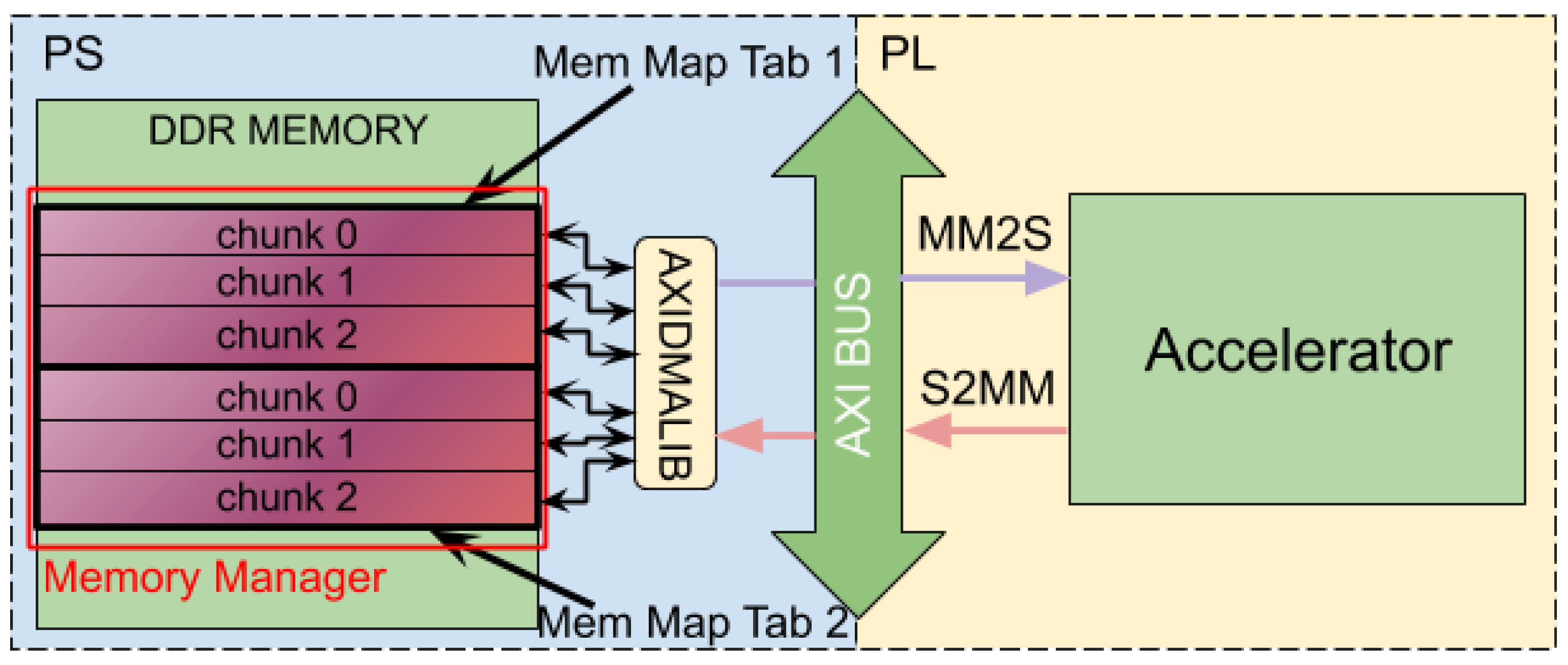
Figure 1 shows an outline of the hardware structure of the PSoC and MPSoC systems. Only those components of these heterogeneous systems that have been used and play a role in the development of this work have been placed in the figure.
Figure 1 shows the two main elements of these systems: PS (left) and PL (right). In PS, there is a processor where a reduced Linux can be run together with specific applications for deep-learning acceleration, which extends the possibilities of embedded systems. They include peripheral controllers, such as USB, that can control many types of sensors, such as cameras or other types of sensors capable of generating images, which can be used as inputs for the FPGA DL accelerator. As in many embedded systems, it has a Direct Memory Access (DMA) controller for the massive movement of data between memory regions of peripherals and memory.
In PL, there is an FPGA that contains several components, such as Configurable Logic Blocks (CLB), block RAMs, Digital Signal Processor (DSP) blocks and serial transceivers, among others, that enable the possibility of designing and implementing a custom hardware to increase the capabilities of the system. All these features, together with the high bandwidth of interconnection between PS and PL, make this system an optimal solution for hardware acceleration.
In order to facilitate the use of all possible needed peripherals on this device, an enhanced Linux-based OS (Petalinux) for embedded systems was used and parametrized for this work. This OS places a software layer over the hardware, enabling a set of drivers to handle the different peripherals that have been enabled in the PS. Among these drivers, two of them play an important role in this work. These is the USB, which is needed for connecting external devices, and the AXI-DMA driver that is needed for large data transfers to and from the PS memory and PL. This work focuses on the study of the AXI-DMA driver used to perform data transfers through the AXI-stream mode. This mode allows sending large data bursts, which is optimal for applications that typically focus on a data-centric and data-flow paradigm, such as hardware acceleration. The driver available in Petalinux for these transfers reserves two clearly differentiated memory areas, one for transfers from PS to PL, called Memory Mapped to Stream (MM2S), and another one for transfers in the opposite direction, i.e., from PL to PS, called Stream to Memory Mapped (S2MM), as shown in
Figure 2. When the driver is configured and the memory areas are defined, its role cannot be changed at runtime. This particularity poses a serious limitation for its use in handling data transfers on NN accelerators, since more flexibility is needed to avoid unwanted memory transfers between these two regions in the PS for preparing the output data of a layer to be transmitted to a new layer. Therefore, data to be sent from an application running on the PS to the accelerator (displayed on the PL) should be copied to the memory area labeled as MM2S. On the other hand, the data generated by the accelerator will be sent and copied to the memory area labeled as S2MM. Once this transfer is completed, the application can access that memory area and read the data. Algorithm 1 shows the steps for the layer-by-layer data transfer of two-layer NN execution.
| Algorithm 1: Transference trace for the execution of a 2-layer NN. |
| 1. | Copy layer 1 configuration data (kernels and biases) to the MM2S area and launch the DMA transfer. Wait until the |
| | transfer is completed. |
| 2. | Copy layer 1 activation data to the MM2S area and launch the transfer. Wait until it is over. At this point the accelerator |
| | starts to generate data (layer 2 activations), sending the data to the S2MM memory area. |
| 3. | Wait until the previous transfer (accelerator to S2MM) is completed. |
| 4. | Copy layer 2 configuration data to the MM2S area and launch the transfer. Wait until the transfer is completed. |
| 5. | Copy layer 2 activation data from S2MM to the MM2S area and launch the transfer. Wait until it is over. At this point |
| | the accelerator starts to generate the output data, sending the data to the S2MM memory area. |
Algorithm 1 shows the number of times that data must be copied to the memory areas defined by the driver. Copying data means moving that data from one memory area to another, which is a waste of time and resources on a task that does not provide any additional value. The NN algorithms handle a large amount of data, and thus these unnecessary data movements in the memory become a drawback.
This work presents an API that improves this deficiency, allowing organizing areas in the memory capable of implementing both roles and being configured at run time, in order to save data movements between memory areas.
3. BiMapTab API
The API proposed in this work consists of a series of classes that allow organizing the memory efficiently in order to define the areas that will be configured in both MM2S and S2MM modes, making it possible to modify their behavior at execution time. In this section, each of the API elements are defined, along with explanations on how the memory is organized to allow performing the transfers efficiently.
The purpose of this API is to provide a physical memory organization, where each area that is reserved can be used to perform bidirectional transfers and, at the same time, provide the virtual pointer to those physical memory areas, allowing them to be used from an application in the user space on a Linux-based OS.
Figure 3 shows the UML diagram of the three main classes (orange shapes) and the struct (blue shape).
3.1. Memory_Manager
This class is in charge of opening the memory map and establishing an area, defined by the memoryOffset and outside the space reserved for the OS, where the different mapping tables will be created. This class has to be instantiated only once, since there would be no purpose in having more than one memory manager, as some mapping tables could be overlapping in the same memory area. Therefore, this class was implemented as a singleton, which allows it to be referenced from any part of the application, although it will only create one instance of the class. This class has two main methods: one used to get or create an instance of this class, getInstance(), and another one used to create a new memory mapping table with a required size, createMapTab(size). Once a new mapping table is created, the memory manager will increase the offset by pointing to the next free memory address where the next mapping table will be created. To maintain proper memory alignment, the size of the mapping tables are created as a multiple of the page size of the OS.
3.2. Chunk
This is a C++ data structure with three attributes: phyPointer, a physical memory address where the data start; virtPointer, a virtual memory address where the data can be accessed; and size, the number of bytes that the data occupy. This is the basic element of the API and will be used to perform the transfers in the system.
3.3. Mem_Mapping_Tab
The instances of this class are created by the memory manager and their purpose is to divide the memory area reserved for the mapping table into small subareas, chunks, where the data are distributed according to the user’s needs. This class has four attributes: phyPointer, a physical address where the memory area reserved for the mapping table starts; virtPointer, the virtual address of the first accessible data; size, the number of bytes reserved for the whole mapping table; and chunks[], a vector of chunks that implements the set of partitions that the user has created in the mapping table. This class has several methods that return the previously defined attributes, although there are two methods of greater importance. The first one, addChunk(size), creates a new element in the chunks[] attribute by returning the recently created chunk to be initialized with the necessary data. The second one, getChunk(id), returns the element at the id position of the chunk[] attribute. Therefore, we can organize the mapping table as needed and access the chunks we need to transfer. All chunks are created consecutively in the mapping table.
3.4. Axidma
This class is responsible for performing transfers via the AXI-DMA controller. When the controller is instantiated in hardware, it is mapped to a memory address, where each of its registers can be accessed in order to check its status and control its actions. To create an instance of this class, it is necessary to know the memory address, axidmaMapAddr, where the controller has been mapped to create the instance referencing such addresses. This class has methods to reset, start and stop the controller as well as write and read methods. The write method performs MM2S transfers, sending data from PS to PL, whereas the read method performs S2MM transfers, sending data from PL to PS. Both methods require the physical address of the memory area where the data will be sent or received as input parameters, as well as the size (in bytes) of the transfer. To send or receive transfers, the only action needed is to call the write or read functions, respectively, using the phyPointer and size of a chunk as parameters.
Figure 4 shows the resulting memory organization by creating two mapping tables in the memory area governed by the memory manager. Three chunks of memory have been created in each mapping table, which can be used to perform transfers through both the MM2S and S2MM channels using the AXI-DMA controller.
The main advantage of the proposed API with respect to the native AXI-DMA Petalinux driver is the possibility of defining memory spaces that support both types of transfers, i.e., from PS to PL and vice versa. Unlike the native driver, once the memory area has been reserved by the Memory_manager, creating a Mem_mapping_tab, this area can be divided into different chunks, which can be used to perform any type of transfer on the fly. To perform the transfer, the Axidma instance requires the physical memory address and the size of the chunk to read (transfer from PL to PS) or write (transfer from PS to PL) the data. To achieve this behavior using the native driver, the same memory area must be reserved indicating the transfer direction for each transaction. Another advantage is the network data organization. Each network layer has two types of data: the configuration (kernel and biases) and the activation data. The proposed API allows the software developer to define different chunks, one for each data type and per layer, simplifying the management of all data and their transfer to the accelerator. In deep learning applications, data management is an intensive task due to the huge amount of data that this kind of algorithms need and generate.
4. Results
To test the performance and versatility of the API proposed in this work, two tests were carried out, in which the performance of the data transfers was measured. The first test, loopback, was an implementation where the MM2S output and S2MM input channels were connected at the PL side (i.e., without the DL accelerator in between). This connection allowed data sent from PS to PL to be sent back from PL to PS without any modification. The second test consisted in an implementation using a hardware accelerator in the PL part, which was fed from the PS, making transfers through the MM2S channel, and the accelerator then sent its result back through the S2MM channel.
4.1. Loopback Test
Two applications were implemented: one using the AXI-DMA native Linux driver and the other using the API proposed in this paper. Both applications performed the same task, generating a series of data in a given memory area and sending these data from PS to PL. These data were sent back from the PL to the PS, and once the data were received, the operation was repeated. This process was carried out 100 times for each transfer size specified in
Table 1. The difference between the native driver and the proposed API resides in the ability to reconfigure the
Mem_mapping_tab elements on the fly, avoiding the data movements between memory areas. In the native driver implementation, when data are received from the PL, it is necessary to move those data from the memory area where they have been received to the memory area used to send data from PS to PL. However, using the proposed API, it is not necessary to move these data since both memory areas can be used for both types of transfers.
Table 1 shows the results of both the Linux native driver and the software API proposed in this work, for eight different transfer sizes. In each cell, two measurements (in milliseconds) can be seen: the first one is for writing transfers (PS to PL) and the second one is for reading transfers (PL to PS). As can be observed, the read transfers are slightly longer than the write transfers for the same transfer size. This is due to the way in which time is measured. For writing, time is measured in PS, which is where the transfer is launched. Therefore, time is measured from right before the transfer is made until the transfer is completed. On the other hand, for reading, the transfer is launched from PL, but time is measured in PS by the test application under execution, i.e., time is measured from right before launching the read command until the transfer is completed. However, there is a delay time between the command launch and the actual start of the transfer from PL to PS. The results show that the proposed API achieved a 85% speedup with respect to the Linux driver.
In addition to the software transference comparison, two Xilinx commercial platforms were evaluated: Zynq PSoC, using the commercial platform Mini Module Plus from Avnet, which holds a 1 GB DDR3 SDRAM, and ZynqU+ MPSoC, using the commercial platform UltraSOM+ MPSoC from Trenz, which holds a 4 GB DDR4 SDRAM. The time difference between the Zyqn PSoC and ZynqU+ MPSoC platforms is due to the high performance port where the AXI-DMA module is connected and the SDRAM technology. In the ZynqU+ MPSoC platform this port is 128 bits, whereas in the previous version, it is 64 bits.
4.2. Accelerator Integration Test
In this test, our API was integrated into the software of a CNNs accelerator [
10], deployed in the PL and put to work at 60MHz in order to process a CNNs trained to recognize the hand gestures used in the game Roshambo [
20] (“rock, paper, scissors”). Like the vast majority of accelerators, the NN operations are processed layer by layer. This NN consists of five convolution layers (pooling and Rectified Linear Unit (ReLU) are also included in each layer), and thus two mapping tables were defined: one for the configuration parameters of each layer (biases and kernels) and another one for the activation parameters. In the first mapping table, five chunks of memory were created where the configuration data of the five layers are initially be copied. In the second mapping table, two chunks of memory were created, which are used for the activation parameters. Initially, the activation parameters of the first layer are copied into the first chunk of memory of this mapping table, using the second chunk to collect the results produced by the accelerator, which correspond to the activation parameters of the next layer. In the next cycle, the second chunk of memory (where the result produced by the accelerator was stored) is used to send the activation parameters to the accelerator, using the first chunk of memory to collect the results produced by the accelerator. This mechanism avoids having to move data within memory, which does not generate any benefit.
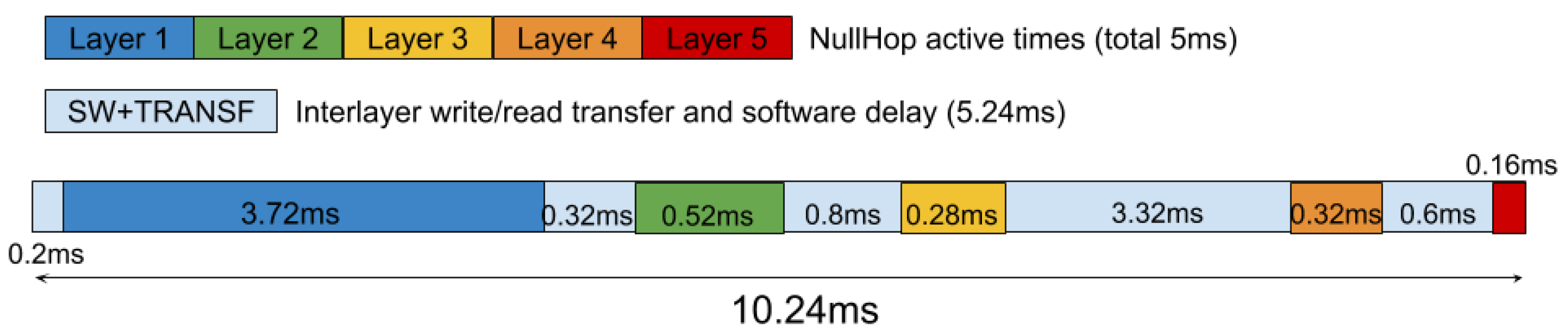
Figure 5 shows the NN execution scheme using the AXI-DMA native Linux driver. It includes the computation time that the accelerator spends on each layer, as well as the transfer time of both the activation parameters and the configuration data for each layer. As can be seen, the data transfer time plus the execution time of the software that controls the accelerator is greater than the total time that the accelerator requires to perform the calculations of the entire network. The total time for computing a frame is 10.24 ms. When replacing the native driver by the API proposed in this work, the time required to compute a complete frame is 8 ms, obtaining an acceleration of 28%.
This paper focuses on the development of an API for AXI-DMA transfers on Zynq and Zynq+ devices governed by an OS. There is another alternative to the OS called BareMetal, which is similar to the workflow of conventional microcontrollers. The resulting software runs on the PS using all of its computing power, since it is the only process that is running on the core. BareMetal allows a more dedicated use of the system’s resources in order to achieve higher performance, but it offers little flexibility and versatility. In [
21], a comparison is made in terms of execution time and performance of an RNN accelerator between both alternatives, BareMetal and Petalinux. That work shows that the difference in time and performance between the two alternatives is feasible, and highlights the advantages offered by the integration of the OS into the system.
On the other hand, in
Table 2, a qualitative and quantitative comparison is shown for when there is a need to perform data movements in memory. If the mechanism for carrying out transfers does not support both directions, the transfer time increases considerably due to the movement of data from one memory area to another.

 ,
, 


