Synchronous Counter Design Using Novel Level Sensitive T-FF in QCA Technology

Abstract
:1. Introduction
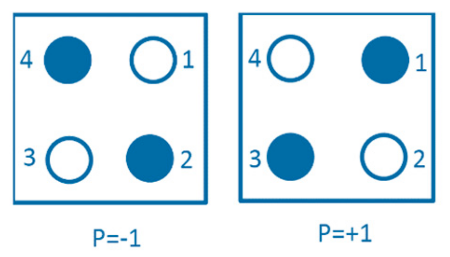
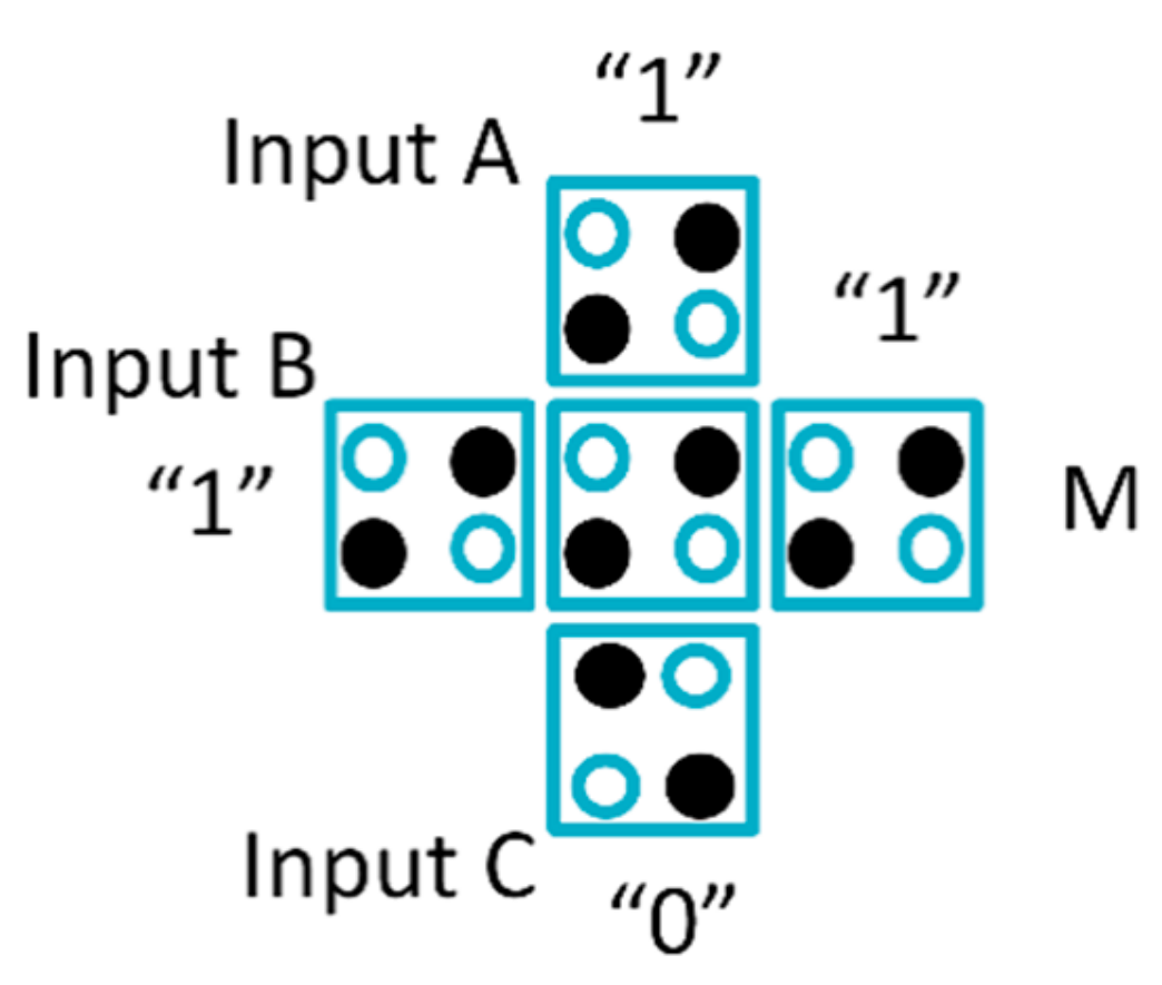
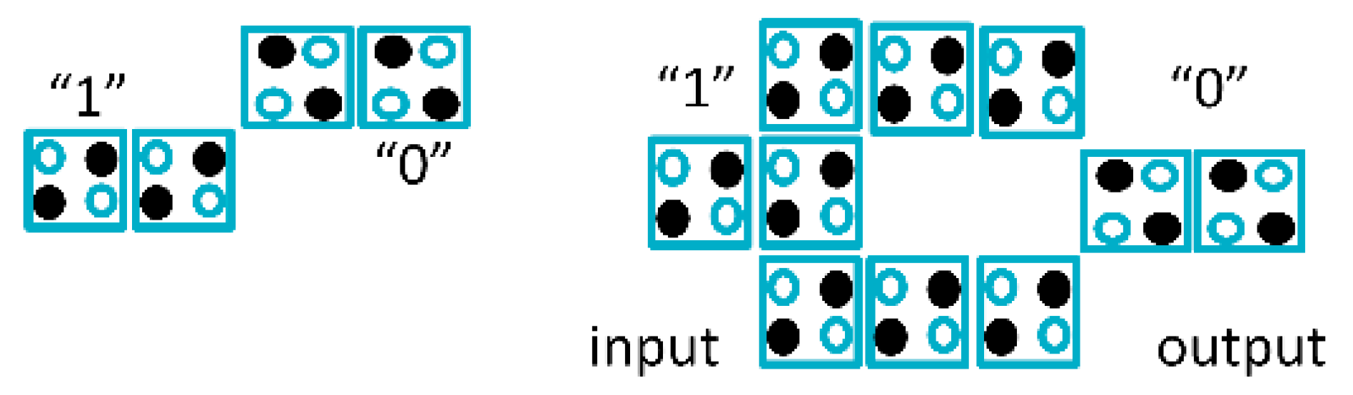
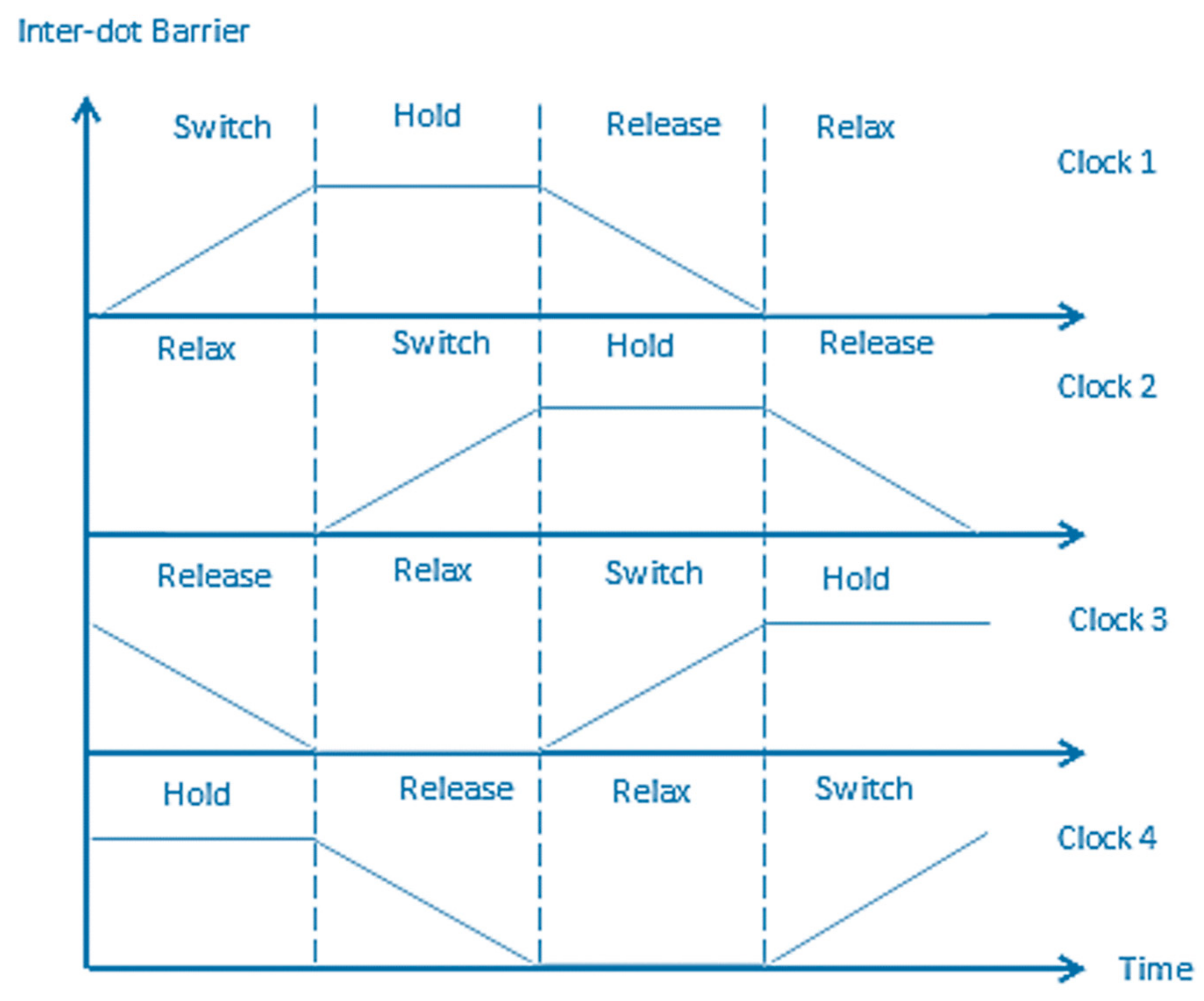
2. QCA Fundamentals
3. Previous Works
4. Proposed Design
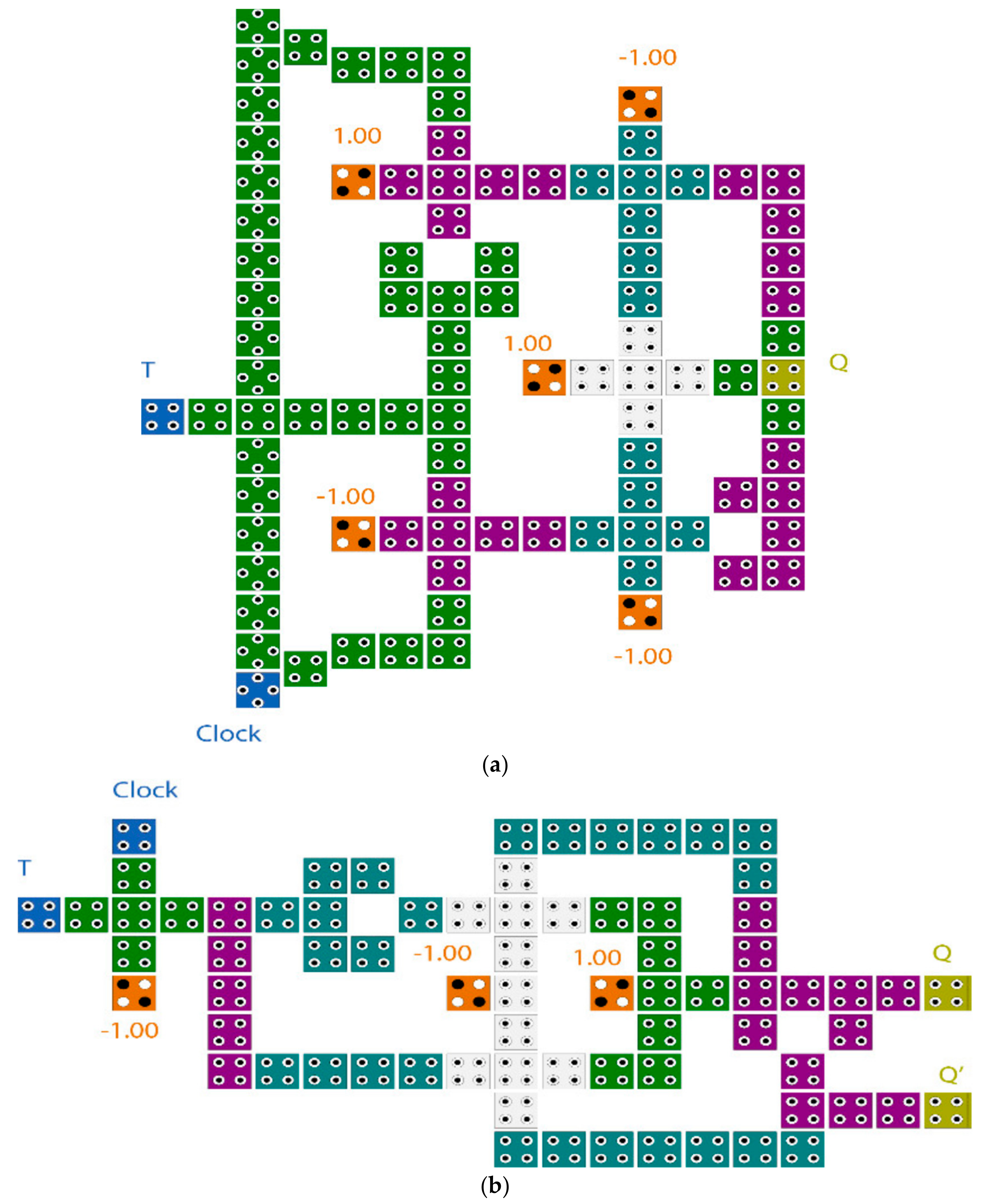
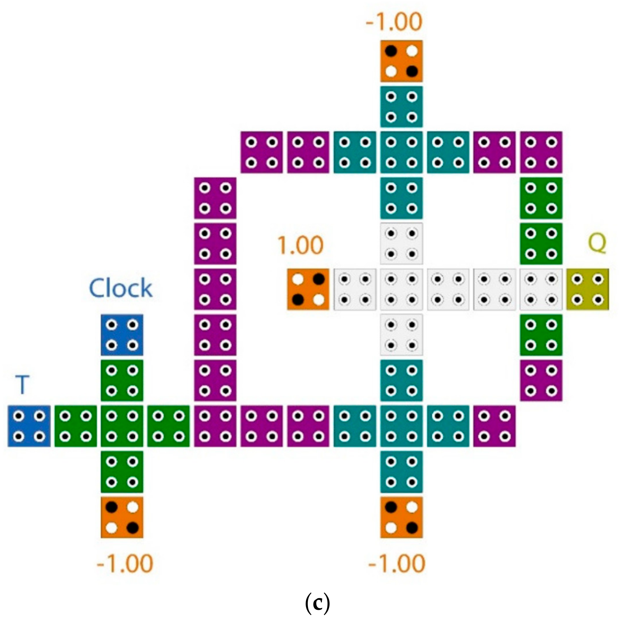
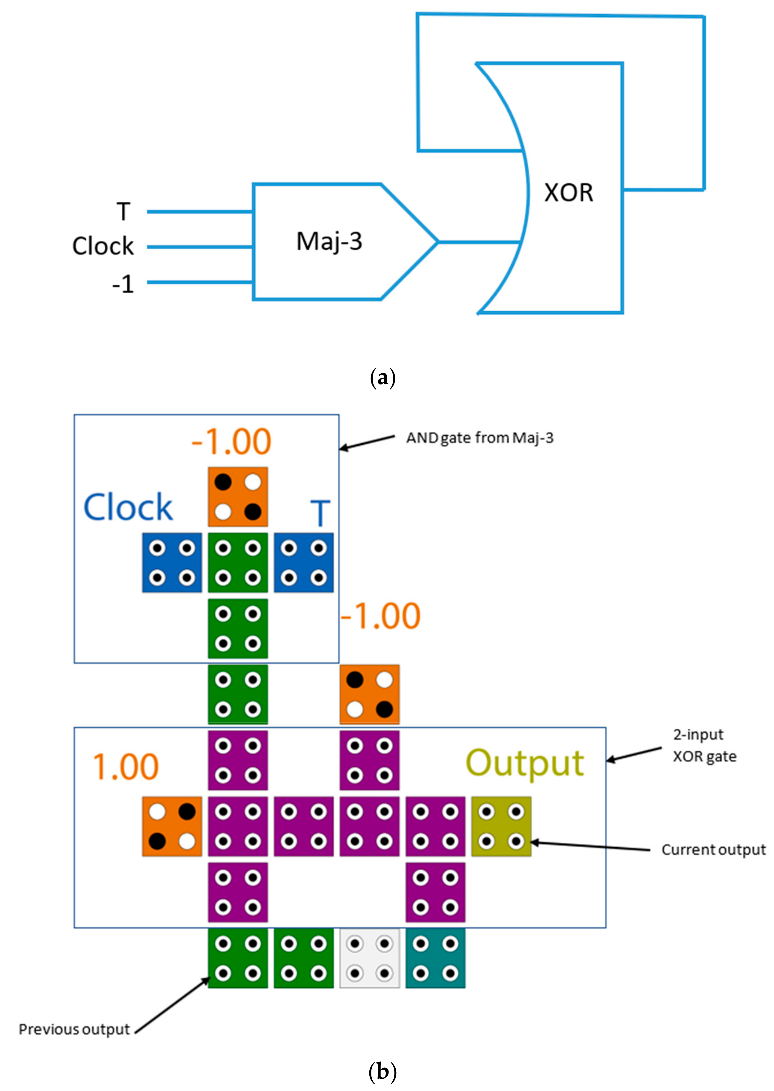
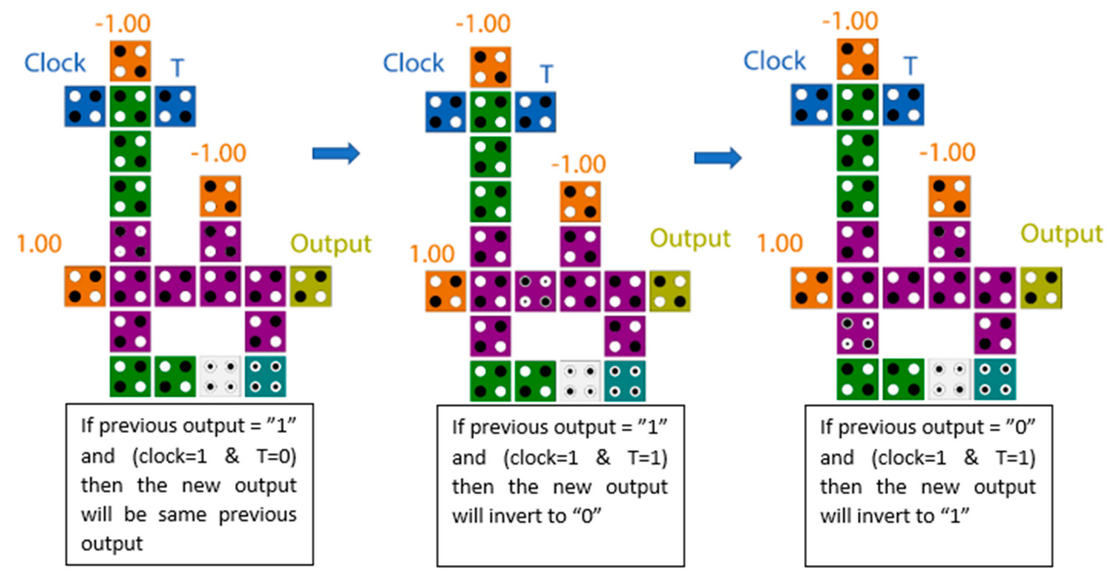
4.1. T Flip-Flop
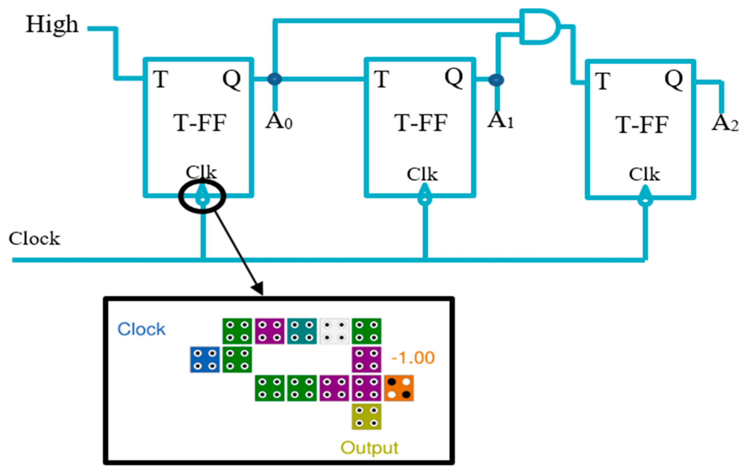
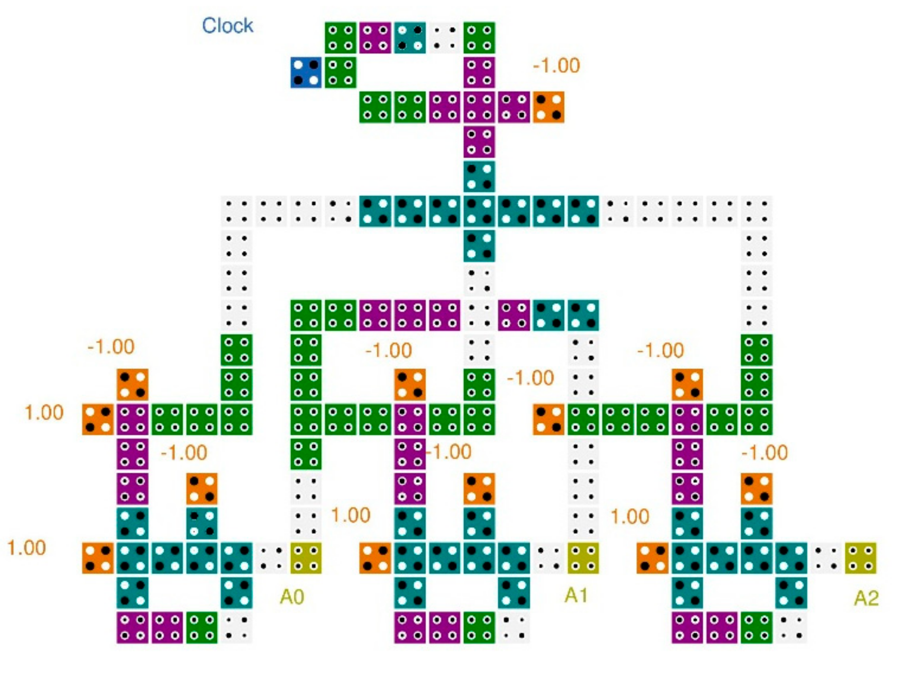
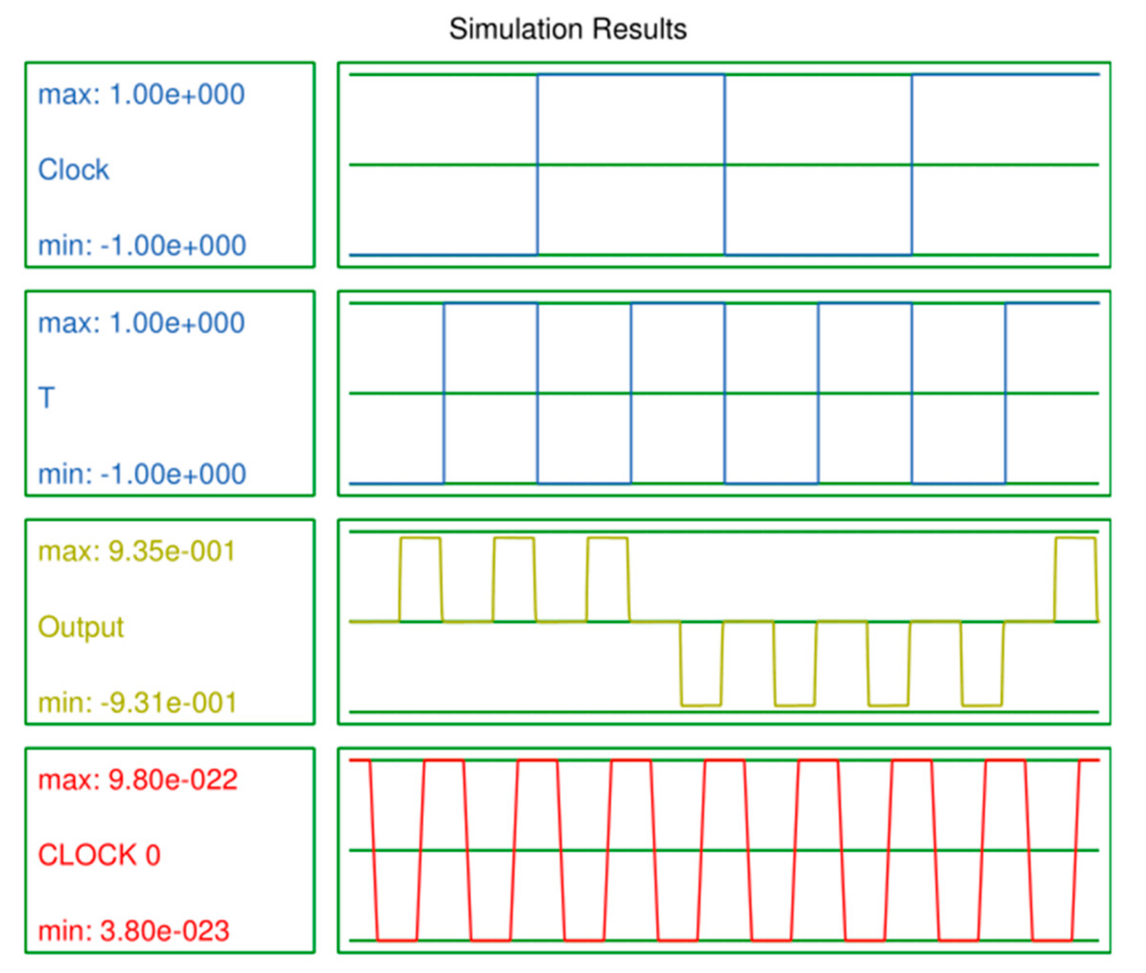
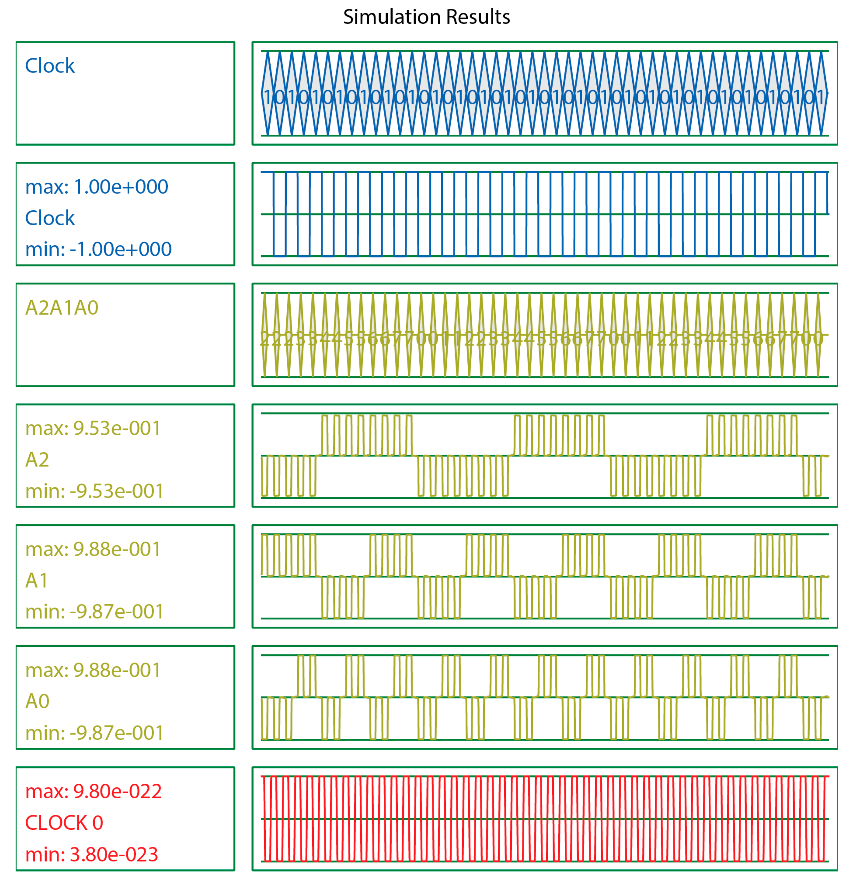
4.2. Synchronous Counter
5. Simulation Results and Comparison
6. Power Analysis
7. Conclusions
Author Contributions
Funding
Conflicts of Interest
References
- Lent, C.S.; Tougaw, P.D.; Porod, W.; Bernstein, G.H. Quantum cellular automata. Nanotechnology 1993, 4, 49–57. [Google Scholar] [CrossRef]
- Dehkordi, M.A.; Shamsabadi, A.S.; Ghahfarokhi, B.S.; Vafaei, A. Novel RAM cell designs based on inherent capabilities of quantum-dot cellular automata. Microelectron. J. 2011, 42, 701–708. [Google Scholar] [CrossRef]
- Hashemi, S.; Navi, K. New robust QCA D flip flop and memory structures. Microelectron. J. 2012, 43, 929–940. [Google Scholar] [CrossRef]
- Angizi, S.; Sarmadi, S.; Sayedsalehi, S.; Navi, K. Design and evaluation of new majority gate-based RAM cell in quantum-dot cellular automata. Microelectron. J. 2015, 46, 43–51. [Google Scholar] [CrossRef]
- Walus, K.; Vetteth, A.; Jullien, G.A.; Dimitrov, V.S. RAM Design Using Quantum-Dot Cellular Automata. Nano Technol. Conf. 2002, 2, 160–163. [Google Scholar]
- Khosroshahy, M.B.; Moaiyeri, M.H.; Navi, K.; Bagherzadeh, N. An energy and cost efficient majority-based RAM cell in quantum-dot cellular automata. Results Phys. 2017, 7, 3543–3551. [Google Scholar] [CrossRef]
- Asfestani, M.N.; Heikalabad, S.R. A novel multiplexer-based structure for random access memory cell in quantum-dot cellular automata. Phys. B Condens. Matter 2017, 521, 162–167. [Google Scholar] [CrossRef]
- Bhavani, K.S.; Alinvinisha, V. Utilization of QCA based T flip flop to design counters. In Proceedings of the 2015 International Conference on Innovations in Information, Embedded and Communication Systems (ICIIECS), Coimbatore, India, 19–20 March 2015; pp. 1–6. [Google Scholar]
- Yang, X.; Cai, L.; Zhao, X.; Zhang, N. Design and simulation of sequential circuits in quantum-dot cellular automata: Falling edge-triggered flip-flop and counter study. Microelectron. J. 2010, 41, 56–63. [Google Scholar] [CrossRef]
- Angizi, S.; Moaiyeri, M.H.; Farrokhi, S.; Navi, K.; Bagherzadeh, N. Designing quantum-dot cellular automata counters with energy consumption analysis. Microprocess. Microsyst. 2015, 39, 512–520. [Google Scholar] [CrossRef]
- Sheikhfaal, S.; Navi, K.; Angizi, S.; Navin, A.H. Designing High Speed Sequential Circuits by Quantum-Dot Cellular Automata: Memory Cell and Counter Study. Quantum Matter 2015, 4, 190–197. [Google Scholar] [CrossRef]
- Navi, K.; Farazkish, R.; Sayedsalehi, S.; Azghadi, M.R. A new quantum-dot cellular automata full-adder. Microelectron. J. 2010, 41, 820–826. [Google Scholar] [CrossRef]
- Navi, S.S.K.; Farazkish, R.; Azghadi, M.R. Five input majority gate, a new device for quantum-dot cellular automata. J. Comput. Theor. Nanosci. 2010, 7, 1546–1553. [Google Scholar] [CrossRef]
- Akeela, R.; Wagh, M.D. A Five-input Majority Gate in Quantum-dot Cellular Automata. NSTI Nanotech 2011, 2, 978–981. [Google Scholar]
- Roohi, A.; Khademolhosseini, H.; Sayedsalehi, S.; Navi, K. A symmetric quantum-dot cellular automata design for 5-input majority gate. J. Comput. Electron. 2014, 13, 701–708. [Google Scholar] [CrossRef]
- Majeed, A.H.; AlKaldy, E.; bin Zainal, M.S.; Nor, D.B.M. A new 5-input Majority Gate Without Adjacent Inputs Crosstalk Effect in QCA Technology. Indones. J. Electr. Eng. Comput. Sci. 2019, 14, 1159–1164. [Google Scholar] [CrossRef]
- Vankamamidi, V.; Ottavi, M.; Lombardi, F. A line-based parallel memory for QCA implementation. IEEE Trans. Nanotechnol. 2005, 4, 690–698. [Google Scholar] [CrossRef]
- Angizi, S.; Alkaldy, E.; Bagherzadeh, N.; Navi, K. Novel Robust Single Layer Wire Crossing Approach for Exclusive OR Sum of Products Logic Design with Quantum-Dot Cellular Automata. J. Low Power Electron. 2014, 10, 259–271. [Google Scholar] [CrossRef]
- Alkaldy, E.; Eshghi, M.; Kadhom, L.; Navi, K. Quantum Dot Cellular Automata models using VHDL-AMS. J. Babylon Univ. 2014, 22, 54–59. [Google Scholar]
- Angizi, S.; Sayedsalehi, S.; Roohi, A.; Bagherzadeh, N.; Navi, K. Design and Verification of New n-Bit Quantum-Dot Synchronous Counters Using Majority Function-Based JK Flip-Flops. J. Circuits Syst. Comput. 2015, 24, 1550153. [Google Scholar] [CrossRef]
- Vetteth, A.; Walus, K.; Dimitrov, V.S. Quantum-dot Cellular Automata of Flip Flops. ATIPS Labrotary 2003, 2500, 1–5. [Google Scholar]
- Torabi, M. A new architecture for T flip flop using quantum-dot cellular automata. In Proceedings of the 2011 3rd Asia Symposium on Quality Electronic Design (ASQED), Kuala Lumpur, Malaysia, 19–20 July 2011; pp. 296–300. [Google Scholar]
- Chen, H.; Lv, H.; Zhang, Z.; Cheng, X.; Xie, G. Design and Analysis of a Novel Low-Power Exclusive-OR Gate Based on Quantum-Dot Cellular Automata. J. Circuits Syst. Comput. 2019, 0, 1950141. [Google Scholar] [CrossRef]
- Xiao, L.R.; Xu, X.; Ying, S.Y. Dual-Edge Triggered T Flip-Flop Structure Using Quantum-Dot Cellular Automata. Adv. Mater. Res. 2013, 662, 562–567. [Google Scholar] [CrossRef]
- Ai, L.L.; Ghazali, A.; Yan, S.C.T.; Chien, F.C. Sequential circuit design using Quantum-dot Cellular Automata (QCA). In Proceedings of the 2012 IEEE International Conference on Circuits and Systems (ICCAS), Kuala Lumpur, Malaysia, 3–4 October 2012; pp. 162–167. [Google Scholar]
- Chakrabarty, R.; Mahato, D.K.; Banerjee, A.; Choudhuri, S.; Dey, M.; Mandal, N.K. A novel design of flip-flop circuits using quantum dot cellular automata (QCA). In Proceedings of the 2018 IEEE 8th Annual Computing and Communication Workshop and Conference (CCWC), Las Vegas, NV, USA, 8–10 January 2018; pp. 408–414. [Google Scholar]
- Angizi, S.; Navi, K.; Sayedsalehi, S.; Navin, A.H. Efficient Quantum Dot Cellular Automata Memory Architectures Based on the New Wiring Approach. J. Comput. Theor. Nanosci. 2014, 11, 2318–2328. [Google Scholar] [CrossRef]
- Abutaleb, M.M. Robust and efficient quantum-dot cellular automata synchronous counters. Microelectron. J. 2017, 61, 6–14. [Google Scholar] [CrossRef]
- Amirzadeh, Z.; Gholami, M. Counters Designs with Minimum Number of Cells and Area in the Quantum-Dot Cellular Automata Technology. Int. J. Theor. Phys. 2019, 58, 1758–1775. [Google Scholar] [CrossRef]


| T | Clock | Current Output (Qt) |
|---|---|---|
| 0 | 0 | Qt-1 |
| 0 | 1 | Qt-1 |
| 1 | 0 | Qt-1 |
| 1 | 1 | Qt-1 |
| Previous Clock | Current Clock | Output |
|---|---|---|
| 0 | 0 | 0 |
| 1 | 0 | 1 |
| 0 | 1 | 0 |
| 1 | 1 | 0 |
| Design | Cell Counts | Area (µm2) | Latency |
|---|---|---|---|
| [24] | 184 | 0.32 | 3 |
| [25] | 108 | 0.20 | 1.5 |
| [21] | 92 | 0.10 | 1.25 |
| [26] | 81 | 0.07 | 1.5 |
| [22] | 66 | 0.06 | 1.25 |
| [27] | 55 | 0.06 | 1.5 |
| [10] | 46 | 0.06 | 1 |
| Proposed | 21 | 0.0186 | 0.5 |
| Design | No. of Bit | Cell Counts | Area (µm2) | Latency | Layer Required |
|---|---|---|---|---|---|
| [9] | 2 | 328 | 0.62 | 3 | Single |
| 3 | 616 | 1.2 | 5 | Single | |
| 4 | 1130 | 2.2 | 7 | Single | |
| [11] | 2 | 240 | 0.26 | 2 | Multi |
| 3 | 428 | 0.48 | 2 | Multi | |
| 4 | 652 | 0.74 | 2 | Multi | |
| [10] | 2 | 141 | 0.22 | 2.25 | Single |
| 3 | 238 | 0.36 | 2.25 | Single | |
| 4 | 354 | 0.49 | 2.25 | Single | |
| [28] | 2 | - | - | - | - |
| 3 | 196 | 0.22 | 4 | Single | |
| 4 | - | - | - | - | |
| [29] | 2 | - | - | - | - |
| 3 | 174 | 0.20 | 3 | single | |
| 4 | 258 | 0.25 | 4 | single | |
| Proposed | 2 | 80 | 0.09 | 2 | Single |
| 3 | 140 | 0.16 | 2 | Single | |
| 4 | 196 | 0.24 | 2 | Single |
| Circuit Presented in | Average of Leakage Energy Dissipation (meV) | Average of Switching Energy Dissipation (meV) | Total Energy Consumption (meV) | ||||||
|---|---|---|---|---|---|---|---|---|---|
| 0.5Ek | 1Ek | 1.5Ek | 0.5Ek | 1Ek | 1.5Ek | 0.5Ek | 1Ek | 1.5Ek | |
| [21] | 45.67 | 131.9 | 231.18 | 90.75 | 79.16 | 67.86 | 136.42 | 211.06 | 299.04 |
| [27] | 19.23 | 53.9 | 93.58 | 36.23 | 30.76 | 25.83 | 55.46 | 84.66 | 119.41 |
| [22] | 22.48 | 67.46 | 120.46 | 66.24 | 58.25 | 50.13 | 88.72 | 125.71 | 170.59 |
| [10] | 15.76 | 44.91 | 78.23 | 15.6 | 13.49 | 11.49 | 31.36 | 58.4 | 89.72 |
| proposed | 6.27 | 18.49 | 32.67 | 22.94 | 19.72 | 16.73 | 29.22 | 38.22 | 49.40 |
© 2019 by the authors. Licensee MDPI, Basel, Switzerland. This article is an open access article distributed under the terms and conditions of the Creative Commons Attribution (CC BY) license (http://creativecommons.org/licenses/by/4.0/).
Share and Cite
Majeed, A.H.; Alkaldy, E.; bin Zainal, M.S.; Bin MD Nor, D. Synchronous Counter Design Using Novel Level Sensitive T-FF in QCA Technology. J. Low Power Electron. Appl. 2019, 9, 27. https://doi.org/10.3390/jlpea9030027
Majeed AH, Alkaldy E, bin Zainal MS, Bin MD Nor D. Synchronous Counter Design Using Novel Level Sensitive T-FF in QCA Technology. Journal of Low Power Electronics and Applications. 2019; 9(3):27. https://doi.org/10.3390/jlpea9030027
Chicago/Turabian StyleMajeed, Ali H., Esam Alkaldy, Mohd Shamian bin Zainal, and Danial Bin MD Nor. 2019. "Synchronous Counter Design Using Novel Level Sensitive T-FF in QCA Technology" Journal of Low Power Electronics and Applications 9, no. 3: 27. https://doi.org/10.3390/jlpea9030027