1. Introduction
The rapid scaling of silicon technology has enabled designers to integrate millions and even billions of transistors into a single chip. This ability, to achieve very high integration density, has contributed to the success of integrated circuit (IC) design during the past few decades. Unfortunately, technology scaling is leading to a significant increase in process variability due to random doping effects, imperfections in lithographic patterning of small devices, and related effects [
1]. Process variations (PVs) introduce statistical inter-die/intra-die fluctuations both in physical properties (e.g., transistor threshold voltage and transconductance, interconnect resistances and capacitances) and geometries of the different layers, which in turn result in uncertainties in speed and power characteristics of ICs [
2,
3]. This potentially impacts the parametric yield in advanced process technologies (like the 45 nm and beyond technological nodes) [
2]. Moreover, the yield loss is also expected to grow in the future technology nodes where physical device parameters will approach the atomic scale and therefore will be subject to atomic uncertainties [
1].
PVs can be compensated by using appropriate circuit techniques like Adaptive Body Bias (ABB) and Adaptive Supply Voltage (ASV) [
4]. The ABB technique is based on the use of the transistor body effect to change transistor threshold voltage during circuit operation. This is accomplished by applying an adaptive body bias (either forward or reverse bias) to the transistors belonging to an IC. In [
5] the effectiveness of ABB methodology was demonstrated. Body biasing was applied to both
n-channel and
p-channel transistors through separate on-chip power distribution networks. The
p-channel transistors were forward biased to improve performance, whereas the
n-channel transistors were reversed biased to reduce leakage. Results obtained in [
5] demonstrate that the ABB technique can be very effective to control the distribution of maximum operating frequency (F
max) and maximum power consumption (P
max), and thus, to improve the parametric yield.
Another well known method for performing PV compensation is the ASV approach which consists in opportunely tuning the power supply voltage (VDD). This technique was originally proposed to trade performance with power [
6,
7]. In addition, as demonstrated in [
4], the ASV method can be also a very good choice to tighten the performance and power consumption distributions and to improve product yield. Moreover, from the cost perspective, the ASV scheme is a less expensive solution than the ABB scheme, since ABB requires additional routing resources to distribute the bias voltage [
4].
Whereas the above mentioned design methodologies are effective for compensating inter-die PVs they are less useful to mitigate intra-die PVs, since it is not physically possible to measure the variations for each single transistor on the chip and generate and apply the appropriate body/VDD source voltage to it.
The most well-known technique for reducing device-to-device (
i.e., intra-die) random variations consists of increasing the size of the transistors. However, in digital circuits this approach can lead to considerable power and area overheads [
1].
In this paper, the influence of intra-die random PVs is analyzed considering the particular case of the adder circuits, which are a very important class of digital circuits since they are frequently used in the critical path of the control unit and the data-path of microprocessors and digital signal processors (DSPs) [
8–
10].
As a first step of our analysis, the speed uncertainty due to PVs is evaluated for different power supply voltages. It is shown that the impact of intra-die PVs on delay strongly depend on the considered VDD. Moreover the delay sensitivity worsens at the lower supply voltages. This information is particular important, especially for low power applications where the supply voltage may be reasonably low. In fact, if the delay variation becomes too large, timing yield fallout may occur. As a subsequent step of this work, the sensitivity to process variations was comparatively analyzed for low-energy slow and high-energy fast adder architectures. As a fundamental result, our study demonstrates that, for an equal energy budget, low-complexity circuits operating at higher VDDs can be significantly faster and less delay sensitive to random PVs than high-complexity adders operating at lower power supply voltages. This suggests some criteria for opportunely choosing optimum VDD and logic architecture to design energy aware high yield adders. We believe that this result can be very useful as it provides effective suggestions to manage intra-die process variability impact on Deep-Submicron (DSM) multi-VDD digital systems.
This paper is organized as follows: in Section 2, the analyzed adder topologies are briefly reviewed and their main characteristics are discussed; Section 3 deals with the impact of intra-die process variability on the analyzed adders; timing yield issues and important design guidelines for energy-aware adder circuits are discussed in Section 4; finally, conclusions are drawn in Section 5.
2. Adder Circuits and Nominal Performances
Addition of binary numbers is implemented in a bitwise approach. At each bit position, the sum value can be determined based upon the corresponding bit values of the operands and the incoming carry value from the previous position. Since, in the worst case, the incoming carry value should be propagated from the least significant bit position to the most significant, the delay of an addition operation is dependent on the operand word length (
n). In order to reduce addition time, different carry propagation techniques have been proposed at both the logical and circuit level [
10].
Five 16-bit adder architectures have been considered as the case study in this work. They were synthesized by Synopsys Module Compiler (MC) [
11] forcing a speed optimization (by using the
max-delay timing constraint) and exploiting the STMicroelectronics (ST) 45-nm static Low-Power CMOS standard-cells library. The different logic architectures available for the MC automatic synthesis are summarized in
Table 1, which also shows adder delay and area characteristics. The ripple carry adder (
Ripple) is a low-area, slow and low-energy structure. By specifying this kind of architecture, MC maps an alternating polarity chain of full adders with inverted carry-ins and carry-outs [
11].
The fast carry look-ahead (
fast_CLA) adder is the fastest available MC architecture, but it is also the largest. It uses a dense carry tree to propagate the carries to each bit, in only log
2 n inverting AND-OR delays [
11]. The carry look-ahead (
CLA) adder exploits a sparse carry tree that roughly doubles the delay (actually 2(log
2 n – 1)) in the carry tree, relative to the
fast_CLA but it provides significant area savings [
11]. The carry select adder (
CSA) is also a high-performance circuit. However, by increasing the adder size, the growing loading on the carry-select lines can degrade performance below the expected level. The carry look-ahead/select adder (
CLSA) is by far the most flexible architecture (by specifying this kind of architecture MC automatically creates a structure ranging from a
Ripple to a
fast_CLA adder, depending on the desired delay [
11]).
When a digital circuit is designed using the semi-custom standard cells based approach, the available degrees of freedom for a designer to satisfy given energy consumption and performance specs are essentially represented by logic architecture and supply voltage choosing. Among these, tuning the VDD value is a straightforward technique to meet the given delay (energy) constraint. In fact, by increasing the power supply voltage, the device drive currents are improved thus leading to better circuit performances, but this also degrades both dynamic and leakage power which are quadratically and exponentially dependent on VDD, respectively. Conversely, by reducing the power supply voltage, dynamic and leakage power are improved but the performance is degraded.
In order to characterize the sensitivity of the considered adder architectures to different VDDs, the circuits were simulated in the Cadence environment for VDD ranging from 0.8 V up to 1.2 V. Simulations were performed placing input buffers between ideal voltage sources and operand inputs to provide realistic input signals. Moreover, each output signal was loaded with a 0.8 fF capacitance (which corresponds to the input capacitance of a D-type Flip-Flop in the referred technology). This choice allows realistic running conditions to be examined.
Figure 1 compares the nominal performances of the different adder topologies in the considered VDD range. Given simulation results were obtained for the TT 75 °C process corner and plotted for a step of 0.1 V. As expected, the
fast_CLA and the
CLSA achieve lower delay. On the contrary, the
Ripple architecture is the slowest implementation resulting always more than three times slower than the fastest circuit.
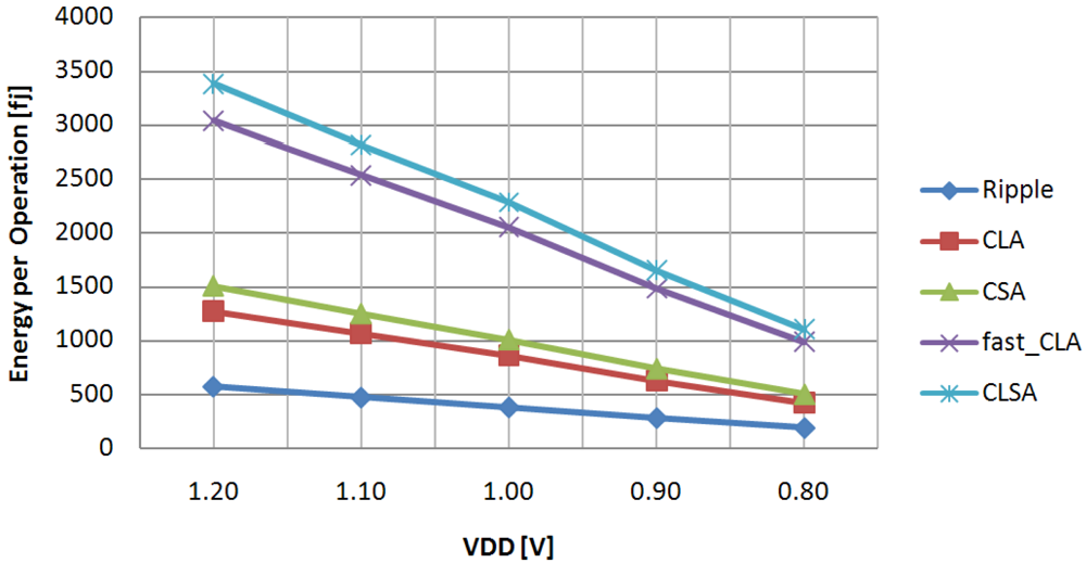
The energy dissipation evaluated under different supply voltages is plotted in
Figure 2. Note that the energy consumption plotted here is an average energy value per operation (
Eop), evaluated over 200 input patterns. The latter were randomly provided at a running frequency of 166 MHz. From
Figure 2, it is easy to observe that the
Ripple circuit exhibits energy consumption significantly lower than the remaining counterparts (
i.e., up to 56%, 62%, 81% and 83% less than the
CLA,
CSA,
fast_CLA and
CLSA, respectively), proving to be the most suitable choice when low power consumption is mandatory. In contrast, the fastest adders (
i.e., the
fast_CLA and
CLSA) are the most energy hungry architectures, thus useful only when speed is the primary concern.
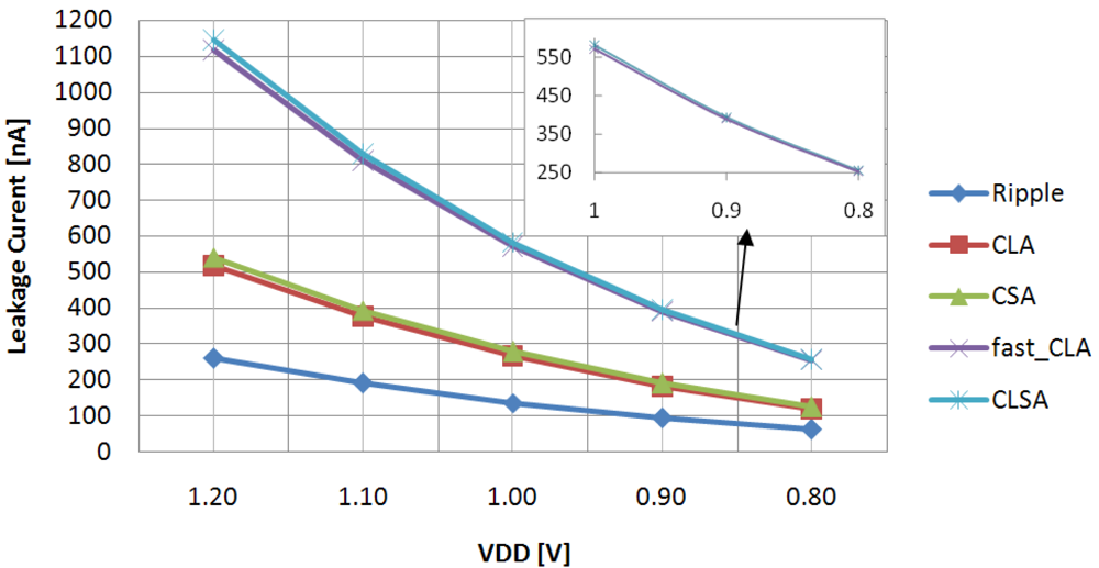
For the sake of completeness, the leakage current evaluated in the considered VDD range is plotted in
Figure 3. The
Ripple circuit shows minimum leakage current due to its low-area structure, whereas relatively high leakage currents were measured for the fastest circuits due to their larger area occupancy.
The analyzed adder topologies can be thoroughly and fairly compared by combining results of
Figure 1 and
Figure 2 in the Energy-Delay (E-D) space (
i.e., the set of design points showing for a given energy/delay value the correspondent delay/energy characteristic), as illustrated in
Figure 4. By opportunely tuning the VDD value, the correct operations of the
Ripple circuit are guaranteed also with energy consumption lower than 420 fJ. This can be obtained by using a power supply voltage equal or lower than the nominal VDD (
i.e., 1 V).
As highlighted in
Figure 5, the
CLA, the
Ripple and the
CSA circuits, offer very similar speed results in the 460–560 fJ energy range, with a small advantage of the
CLA adder which was up to 4% and 6% faster than the
Ripple and the
CSA architectures, respectively). The
CLA is also the fastest circuit for an energy budget up to the 750 fJ. After that, the
CSA is the most suitable adder architecture since it was up to 1.6× and 2.2× faster than the
fast_CLA and the
CLSA, respectively. Finally, when a very high speed is required (
i.e., for a delay constraint lower than 160 ps) the
fast_CLA circuit is the obvious choice at the expense of considerable energy consumption (
i.e., more than 2.5 pJ).
The performed analysis suggests that considering power supply voltage as a tuning parameter, different architecture choices can be performed on the basis of the available energy budget. In the following, we analyze how the possible choices are impacted by random intra-die PVs.
3. Impact of Intra-Die Process Variability for Different Power Supply Voltages
The impact of intra-die PVs was evaluated through Monte Carlo simulations performed on 1000 samples. In this case, driving circuits of the simulation setup are not influenced by random process variations in order to isolate process variability effects on circuits under test.
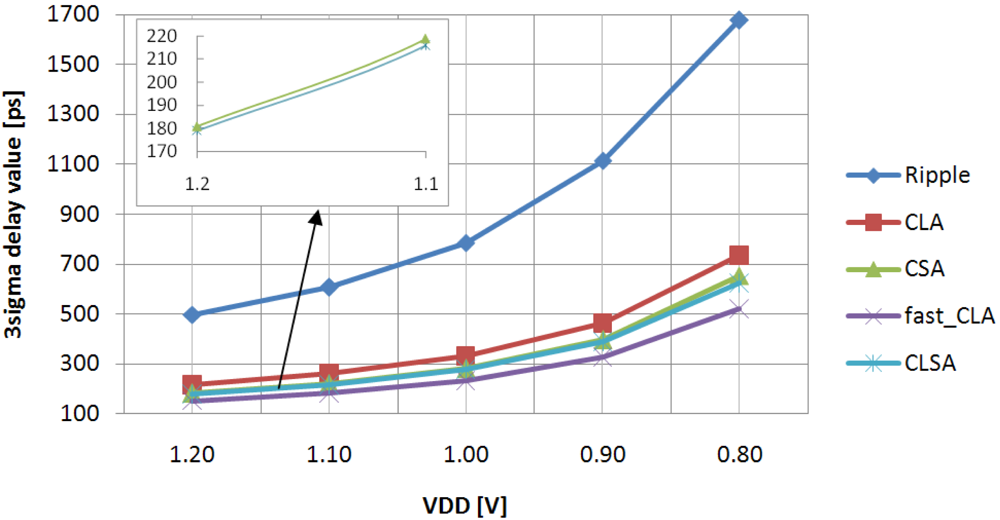
The ratio between the maximum spread 3σ and the mean value μ (
i.e., 3σ/μ [
1]) was considered as a measure of the uncertainty of the delay. As can be easily observed in
Figure 6, during the optimization for power savings (
i.e., VDD lower than the nominal value) the delay variability increases at a rate similar to the decreasing of the nominal delay, and hence timing yield worsens during this optimization. Conversely, the delay variability is reduced for higher power supply voltages. The
Ripple circuit is the less PV delay sensitive circuit (its delay variability ranges from 10.2%@1.2 V to 20.7%@0.8 V). In contrast, the
fast_CLA is the most PV delay sensitive structure (its delay variability spreads from 12.9%@1.2 V to 28%@0.8 V), resulting from 1.26× to 1.35× more delay sensitive with respect the
Ripple architecture. It is interesting to observe that at the same VDD value, circuits with longer critical path lengths always present delay variability lower than those with shorter critical path length. The reduced delay variability of slower circuits is explainable considering the higher number of logic gates which are in the critical path; each of them experiences a different impact on its delay characteristic also with different sign, thus a more pronounced averaging effect exists on longer logic gate chains.
The 3-sigma delay value (defined as μ + 3σ) was evaluated for different VDD and is plotted in
Figure 7.
It is worth noting that the 3-sigma delay value provides very practical information to evaluate the achievable post fabrication timing yield. In fact, considering the 3-sigma delay value as a timing constraint, it is statistically assured that about 99.87% of the fabricated circuits satisfy the target speed [
1]. As the main effect of the intra-die PVs, all the curves are shifted up with respect to those drawn in
Figure 1. Obviously, the experienced shift amount depends on the particular circuit delay sensitivity to intra-die PVs.
Figure 8 compares the Energy-3sigma Delay curves of the different adders. It is worth noting that the average energy consumption per operation is strongly dominated by the switching component which is relatively insensitive to process variations [
12]. For this reason process induced variations on energy can be considered negligible and, thus, they were not taken into account in this work.
Results shown in
Figure 8 describe a quite different scenario with respect to those given in
Figure 4. The E-D curves are now shifted toward the right depending on the influence of process variability on a given adder architecture. Due to this, the
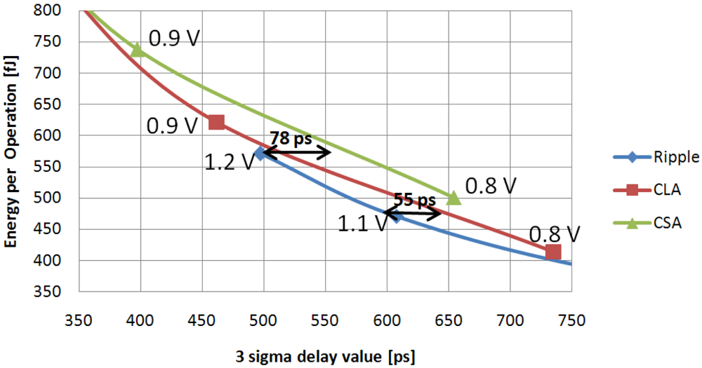
Ripple circuit has the lowest 3-sigma delay value when an energy budget up to 575 fJ is available. This is highlighted in
Figure 9 which plots the
Ripple, the
CLA and the
CSA E-D, curves for energy values ranging from 350 fJ to 800 fJ. It can be seen that the
Ripple architecture can achieve a 3-sigma delay value 9.5% and 16% lower than
CLA and
CSA circuits, respectively. As shown in
Figure 10, the
CLA and the
CSA E-D plots' result almost overlap in the 750–1250 fJ energy range. In the same range these circuits achieve 3-sigma delay up to 46.2% and 59.6% lower than the
fast_CLA and the
CSLA adders, respectively. Although the
fast_CLA presents the highest delay variability, it remains almost the only choice when very high speed is mandatory and energy consumption is not a concern.
The previous discussed analysis provides important suggestions to design robust circuits under energy constraints. This is highlighted in the next section.
4. Timing Yield Issues and Design Guidelines for Energy-Aware Adder Circuits
Under process variations, the delay of a given circuit can be modeled by a normal distribution with a probability density function (PDF) characterized by the mean and the standard deviation values [
1]. By analyzing the PDF of the delay for a given energy constraint, useful information about the achievable timing yield can be obtained.
Figure 11 shows the PDF of the delay for the analyzed adder architectures under the 500 fJ energy constraint. Only the circuits which can meet the energy consumption requirement were considered in this analysis. It can be seen that, for the considered energy point, the
Ripple@1.18 V, the
CLA@0.85 V and the
CSA@0.80 V, can achieve a very similar mean delay. However, as highlighted in
Figure 11, the
Ripple circuit presents a significantly tighter performance distribution due to its delay variability 47% and 57 lower than the
CLA and the
CSA circuits, respectively.
The delay distributions for the
Ripple@1.20 V, the
CLA@1.07 V, the
CSA@1.00 V and the
fast_CLA@0.82 V are plotted for the 1000 fJ energy constraint in
Figure 12. It is worth noting that the
Ripple circuit has been included in the comparison because it can achieve a 3-sigma delay value very close to that of the
fast_CLA architecture working at VDD = 0.82 V (see
Figure 7), while consuming about 43% less energy per operation. As can be observed in
Figure 12, the
CLA and the
CSA presents an almost equal mean delay value which is significantly lower than those of the
fast_CLA (about 39%) and the
Ripple (about 46%) architectures. This higher speed is achieved with relatively low delay variability (
i.e., 12.4% for the
CLA and 14.5% for the
CSA). It is worth noting that the
fast_CLA circuit presents the highest delay variability which is 1.9×, 2.2× and 2.7× larger than that of the
CSA,
CLA and the
Ripple architectures, respectively.
Figure 13 plots the delay PDFs for the
CLA@1.20 V, the
CSA@1.20 V, the
fast_CLA@0.92 V and the
CLSA@0.87 V under the 1500 fJ energy constraint. The
CLA circuit achieves a mean delay value 27% and 47% better than that of
fast_CLA and the
CSLA circuits, respectively. Moreover, the
CLA architecture has the lowest delay variability and consumes about 15% less energy per operation with respect to its counterparts.
The above discussed results clearly demonstrate that, for a given energy constraint, properly power supplied low-complexity adder architectures can achieve better timing characteristics and reduced delay sensitivity to random PVs with respect to complex adders operating at lower power supply voltages.


