Article

Influence of Charge Carriers Concentration and Mobility on the Gas Sensing Behavior of Tin Dioxide Thin Films

1
School of Material Science and Metallurgy, University of Science and Technology Liaoning, Anshan 114051, China
2
State Key Laboratory of Advanced Processing and Recycling of Nonferrous Metals, Lanzhou University of Technology, Lanzhou 730050, China
*
Authors to whom correspondence should be addressed.
Coatings 2019, 9(9), 591; https://doi.org/10.3390/coatings9090591
Submission received: 26 July 2019 / Revised: 7 September 2019 / Accepted: 16 September 2019 / Published: 18 September 2019

Abstract

:
In order to investigate function of carrier behavior on gas-sensing properties, tin oxide-based films with different carrier concentration and mobility were obtained, by magnetron sputtering from the powder target, which was followed by further oxygen-management though the annealing treatment. The microstructure, surface morphology, electrical properties and gas sensitivity were characterized by XRD, Raman spectrum, photoluminescence spectrum, atomic force microscope, the hall effect system and electrochemical workstation, respectively. The results showed that all SnO2-based films had a tetragonal rutile phase with (101) preferred orientation. The introduction of fluorine and regulation of oxygen vacancies tuned carrier concentration from 1015/cm3 to 1021/cm3 and mobility from 102 cm2/V·s to 10−1 cm2/V·s. The decreasing carrier concentration as well as increasing mobility had a positively important function to improve the sensitivity of SnO2-based films. The air-annealed SnO2 film with lowest carrier concentration had a maximum sensitivity of R = 5.0, while vacuum-annealed SnO2:F film with the highest carrier concentration being the minimum sensitivity. This puts forward a novel reference for the design and application of SnO2-based gas sensing films.

1. Introduction

With the requirement of environmental protection and safety, the dangerous, toxic, harmful, flammable and explosive gases need to be detected and regulated, which greatly promoted the development of gas sensor technology. Among many semiconductor materials, tin oxide (SnO2) has been the mainstream of research owing to good chemical stability, fast response/recovery, high sensitivity, low cost and a wide variety of gas responses [1,2,3].
Many studies focus on the synthesis of SnO2-based with different nano sizes and morphologies to improve their adsorption properties, and in turn improve the gas response. By preparing different sizes of SnO2:F nanorod film with spray pyrolysis method, Cho et al. [4] found that nanorod film with a long length of about 370 nm showed relatively higher sensitivity, but a slow gas response and recovery time. Chao et al. [5] reported that the SnO2 nanotubes consisting of 5–10 nm nanoparticles still achieved sensitivity of 16.1% and response time of 20 s, even though under a low-concentration 9.7 ppb NO2 at room temperature. Zhang et al. [6] synthesized SnO2 hollow spheres of different sizes to increase the specific surface area of the sensor, and obtained that the sensitivity to 5–100 ppm NO2 is 8–12.2 times that of solid particles.
Moreover, in order to further improve the sensitivity and selectivity of different nanostructure, many elements including noble metal were doped to increase the active adsorption sites of the sensor. Yin et al. [7] explored the preparation of dual sensors with (Pd, Fe)-modified SnO2 and Pt-loaded SnO2 for improving the gas selectivity, which could detect and calculate the respective concentrations of CO and H2 in the mixed gas. Jin et al. [8] studied that SnO2-based nanostructure by 2.5% doped Cu reached sensitivity of 221 for 500 ppm acetone and increased selectivity between acetone and ammonia, and the corresponding response and recovery times are 9 s and 6 s, respectively. Additionally, Mahdavian et al. [9] and Prades et al. [10] further clarified the interaction of SnO2-based sensors with different kinds of target gases and through simulation calculations.
As a matter of fact, the sensitivity of resistance-typed gas sensor is derived from the change with the resistance of the material [1], which was explained by the molecular reaction model [11] and the grain boundary barrier model [12]. Based on such models, the current researches focused the enhancement of conductance change ΔG by controlling Δn and Δμ of SnO2-based materials, and ignored the effect of initial electrical conductance characteristics about the carrier concentration n0 and mobility μ0.
Here, the SnO2-based dense films with a single preferential orientation were prepared by RF magnetron sputtering to exclude the influence of other factors on carrier transport, in which carrier concentration and mobility were jointly regulated by fluorine doping and oxygen management with annealing. That met the need to study the effect of initial carrier concentration and mobility of SnO2-based films on gas response. Exploration of function on carrier behavior in gas-sensing SnO2-based films would provide a simple and effective criterion for the design and application of sensor in the future.

2. Materials and Methods

In this work, SnO2 film was prepared by a pure SnO2 powdered target, as described in references [13,14]. The fluorine in SnO2:F film was introduced by mechanically mixing the SnF2 powder (99.99%) and the SnO2 powder (99.99%) at an atomic ratio of 1:40. In detail, the glass substrate was dried after a series of ultrasonic cleaning. After the background vacuum of the system was as low as 3 × 10⁻³ Pa, 99.99% argon was introduced to make the operating pressure to 1.0 × 10⁻¹ pa. The gas-sensing films were deposited in a radio frequency (RF, AE600X) magnetron sputtering for 1 h, with a target power of 200 W and a substrate-target separation of 100 mm.
The as-prepared SnO2-based films were annealed at air atmosphere and vacuum of 2.5 × 10⁻³ Pa by rapid thermal processing equipment (RTP-500V) with a rate of 1 °C/s, respectively. Samples were stayed at 110 °C and 200 °C for 5 min to remove adsorbed residues on the surface of the films, and then were kept heating at 400 °C for 1 h. Particularly, annealing at 400 °C may adjust the oxygen vacancy as well as reduce interstitial defects to regulate carrier concentration and mobility. Meanwhile, annealing at 400 °C prevents re-crystallization of the SnO2-based films to maintain the same columnar crystalline structure as the as-prepared samples. In addition, annealing beyond 400 °C can be dangerous to damage the glass substrate to deteriorate structure and property of film.
The parameters including film thickness and deposition rate were obtained through the Profilometry (Alpha-step D-100, Shanghai, China). The micro-crystal structure and electronic band structure were characterized by glancing angle XRD with an incident angle of 0.3° (X-ray diffraction, X’Pert Pro, Almelo, Netherlands, Cu-Kα), Raman spectra (LabRam HR 800, Paris, France) with an excitation wavelength of 532 nm, steady state photoluminescence (PL, FLSP-920, Edinburgh, England) using a 310 nm excitation light and UV-vis light spectrophotometry (Cary 5000/6000i, Beijing, China) with a measuring range of 300–900 nm. Surface morphology and roughness was observed using a field-emission scanning electron microscope (FESEM, Sigma HD, Oberkochen, Germany) at 5 kV and an atomic force microscope (AFM, CSPM5500, Guangzhou, China) by contact mode. Electrical properties including carrier concentration and mobility were recorded at the hall effect measurement system (HALL 8800, Taiwan, China).
The gas response measurements of the films directly assembled and connected to the electrochemical workstation (CHI660B, Chenhua Instruments Inc., Beijing, China) through Al2O3 sheet and Pt wire, were carried out in an electric furnace device equipped with a gas mass flow apparatus. At a constant voltage of 5 V, the “current (I)–time (t) curve” was measured at different temperatures for 2000 ppm different target gases (H2, CO and CH4) in the air ambient. According to Ohm’s law, the resistance was derived from the fixed voltage and the tested current. Response of the films in the paper is defined: R = Ra/Rg, in which Ra and Rg are the resistance values before and after the introduction of the target gas, respectively. The response and recovery time are the consumed time that the resistance value reached or returned to 90% of the previous resistance [15].

3. Results and Discussion

3.1. Composition and Microstructure

3.1.1. X-ray Diffraction

The XRD patterns of the as-prepared and annealed SnO2-based films are shown in Figure 1a. The diffraction peaks of all films are consistent with standard PDF cards (P42/mnm, (136), JCPDF 01-070-4177), and corresponding diffraction planes are (110), (101) and (200), which are from the tetragonal rutile structure SnO2 intensity ratio of (101) peak to other peaks in XRD patterns is higher than that of the standard non-oriented SnO2 powder samples from the above mentioned PDF file, suggesting that all films are the (101) preferred orientation, which is due to the lack of oxygen and the low relaxation ability during sputtering in a pure Ar atmosphere [14,16]. The film with a single orientation effectively simplifies the study of carrier transport on gas-sensing properties.
Besides the original diffraction peak of SnO2 after doping with F, no impurity peaks were observed, and the lattice of the SnO2 after doping remains unchanged, indicating that fluorine atoms is effective doped in SnO2 solid solution. F atom similar with the oxygen atom in size replaces the position of oxygen in the crystal lattice, and plays a role of shallow donor [17]. It provides more carriers to conduction band. In addition, the F doping changes surface energy of different crystal plane, which strengthen the intensity of the preferential (101) peak and suppresses the intensity of (200) peak.
As shown in Figure 1a, the diffraction peak of the SnO2 film after vacuum annealing is much more diffused than that of as-prepared film, which can be explained by the extraction of oxygen atoms under low partial pressure and high temperature. Loss of lattice oxygen releases a large number of carriers to increase conductance. In contrast, the oxygen vacancies in original samples are effectively filled by the atmosphere oxygen during the air-annealing process, which reduce carrier concentration. Meanwhile, the lattice in films is much more perfect to increase the intensity of the (101) peaks as shown in Figure 1a. Particularly, the introduction of fluorine further reduces the intensity of the (101) peak after vacuum annealing, indicating that de-oxidation occurred to a greater extent, because the coulomb force of the bound lattice in SnO2 is weakened by substitution of F [18]. While the atmosphere oxygen is sufficient under air-annealing, the appearance of (110) orientation suppress (101) preferred orientation to some extent.

3.1.2. Raman Spectra

The structural information of SnO2-based films including oxygen vacancies could be detected by Raman spectra [19] as shown in Figure 1b. All samples showed the Raman characteristic vibration of pure phase SnO2 with rutile structures [20], containing Eg (~470 cm−1), A1g (~630 cm−1) and B2g (~775 cm−1). Conforming to the Matossi’s constant, the peak of 371 cm−1 is closely related to the local lattice disorder, and the peak at 570 cm−1 originates from the plane oxygen vacancies, which the greater the relative intensity is, the higher the concentration of the oxygen vacancies is [21].
The integral intensity of the air-annealed SnO2 film at 570 cm−1 is weaker than that of the as-prepared film, as well as the intensity of A1g reflecting the reverse vibration of the Sn–Sn and O–O in the c-axis plane is higher. It indicates that air-annealed films have much less oxygen vacancies. By contrast, de-oxidation of the vacuum-annealed SnO2 film produces more oxygen vacancies due to the relatively higher intensity of the peak at 570 cm−1. The similar change of oxygen vacancies is also presented in F doped SnO2 films before and after annealing.
The F atom replacing the lattice oxygen affected the vibration of the original Sn–O bond, and the intensity of all Raman peaks is reduced to some extent after doping. A1g mode of SnO2:F films have a lower wavenumber compared with undoped samples. It illustrates that the oxygen vacancies in the sample are increased after doping F [21], which reflects the weakened Sn–O binding ability. This also shows that the generation of oxygen vacancies in vacuum annealing is further enhanced by F doping.

3.1.3. Photoluminescence Spectra

As shown in Figure 1c, the photoluminescence (PL) spectra of all samples showed fluorescence emission peaks appear at ~397 nm, ~530 nm and ~710 nm. However, the emission peaks at 620 nm are due to the second-order emission peak of the excitation light that is not filtered out. The UV emission peak near 397 nm (about 3.26 eV) attributed to carrier recombination from the conduction band to the valence band. Moreover, as shown in Figure 1d,e, the optical bandgap width by Tauc extrapolation is about 3.3 eV, which is almost the same as the PL result, and smaller than the band gap (3.6 eV) of SnO2 in the other study [22]. It implies that our SnO2-based films have more charge carriers whose transport behavior could be expected to be tunable. The peak of ~530 nm (2.34 eV) reflects the defect energy level in samples, which is related to the formation of oxygen vacancy [23]. In addition, the peak at 710 nm is usually related to surface defects at grain boundaries [24].
The effective introduction of F atoms makes the photoluminescence intensity significantly lower compared to undoped SnO2 film, which is similar to the result of the references [22]. Doped F in the crystal lattice makes it more difficult for the carrier in the excited state back to the ground state and the luminescence intensity is lower. Moreover, more oxygen vacancies in F-doped films deduced from XRD and Raman analysis should be responsible for the decrease of the photoluminescence intensity [25]. Meanwhile, besides a certain amount of oxygen vacancies and other lattice defects, the introduction of fluorine causes the impurity band to further expand, resulting in an increase in the electron transition range, which leads to the broadening PL peak of the SnO2:F films.
From Figure 1c, both introduction of F atoms and increase of oxygen vacancies make peaks at ~397 nm and ~530 nm blue-shifted, corresponding to the increase of optical band gap. For degenerate semiconductor, there would be a relationship of Equation (1) between band gap width ΔEg (BM) variation and carrier concentration n for the Burstein–Moss effect [26].
Δ E g   =   h 2 2 ( 1 m v + 1 m c )   ( 3 π n ) 2 3 .
In which m v and m c are the effective masses of electron in the conduction band and the valence band, respectively, and h is the Planck constant. As shown in Figure 1f, the band gap variation ΔEg of SnO2-based samples is basically proportional to the 2/3 power of their carrier concentration, which satisfies with the Equation (1). It could be deduced that the Burstein–Moss effect may be available to our degenerate SnO2-based films. Subsequently, the band gap becomes wider as the carrier concentration increases in this study. The co-operation of F atoms or oxygen vacancies would make the film have higher carrier concentration, which is illustrated from blue-shift of F-doped SnO2 film in Figure 1c and the increase of band gap in the vacuum-annealed samples in Figure 1e.

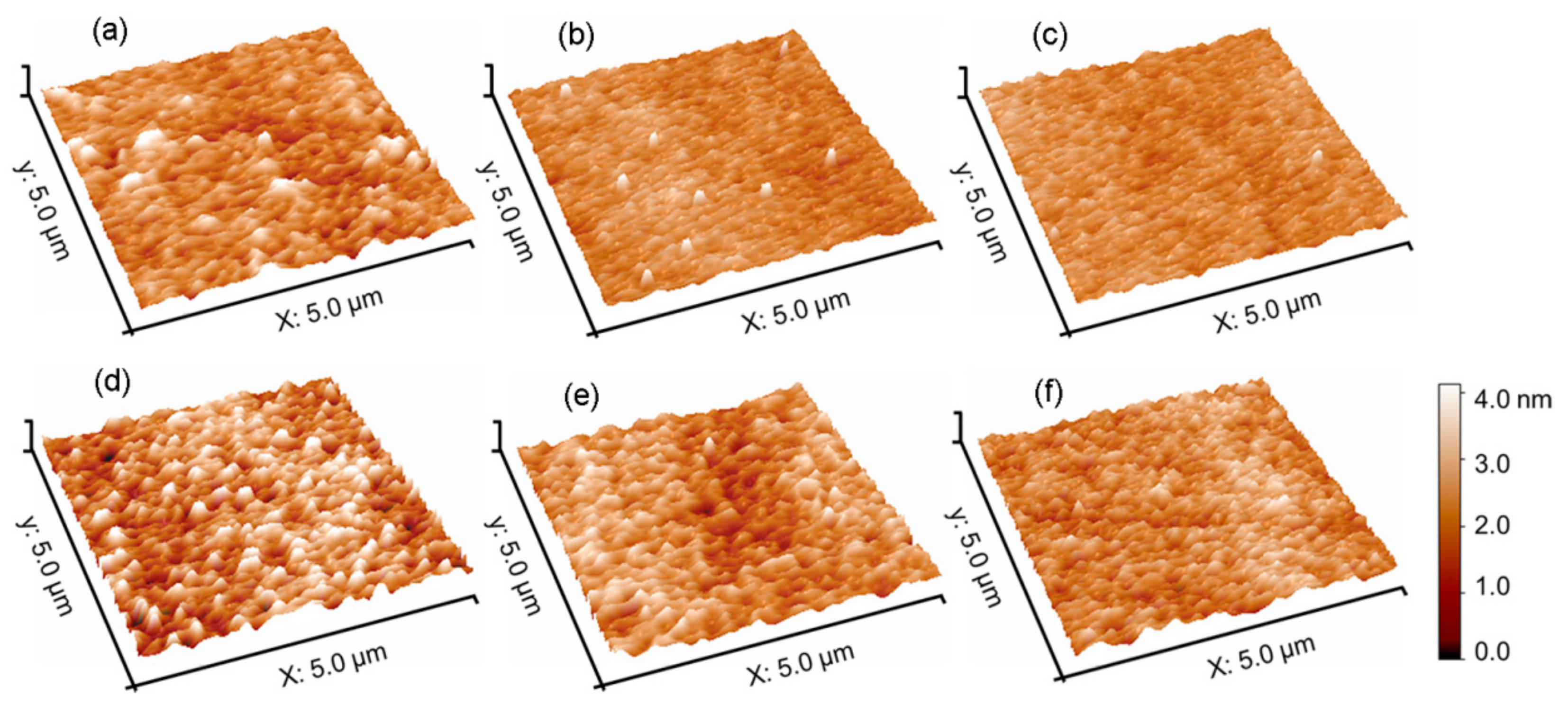
3.2. Surface Morphology

As seen in Figure 2 and Figure 3, the cross-sectional SEM presents the films consisting of columnar crystalline with diameters about 100 nm, which is consistent with the typical microstructure of magnetron sputtered SnO2-based films. The top SEM together with three-dimensional AFM morphology of samples shows that the surfaces of films are dense and smooth. The morphology difference between SnO2 and SnO2:F films originated from the variant etching ability due to the introduction of fluorine in the sputtering process. It is obvious that the as-prepared SnO2-based films have a roughness of only about 4.1 nm in Figure 2 and Table 1. Furthermore, the film surface is smoothed by the rounded top of the column grain during the annealing process. Moreover, the film annealed under ambient air has the lowest roughness owing to the supplement of oxygen. In addition, it can also be seen from Figure 3a,e to Figure 3c,f that the image contrast of the surface morphology gradually becomes unobvious, which is due to the smoother sample surface and the lower electrical conductivity deteriorated by the introduction of oxygen.

3.3. Electrical Properties

The oxygen vacancies of SnO2 as an N-type semiconductor may play an important role in its electrical transport properties, by forming an impurity level to release free electrons to conduction band. Through oxygen introduction in air-annealing and oxygen extraction in vacuum-annealing, the number of oxygen vacancies could be simply regulated in a wide range, and in turn change carrier concentration from 1015/cm3 to 1019/cm3 as shown in Table 1. However, the carrier mobility decrease from 102 cm2/V·s to 10−1 cm2/V·s results from scattering of lattice distortion owing to the increase of oxygen vacancy. It is well known that resistivity ρ, carrier concentration n and mobility μ have the relationship ρ = 1/nqμ. The resistivity of SnO2 mainly depends on the carrier concentration and mobility. As can be seen from the data in Table 1, resistivity and carrier concentration show a positive correlation regardless of mobility. Therefore, the effect of carrier concentration on resistivity is stronger than that of mobility.
F-doped is also another way to adjust the electrical properties of SnO2-based materials by increasing the carrier concentration. According to equation Oo + F→F’ + e + 1/2O2 (g), fluorine occupies the position of the oxygen atom and releases a free electron [27]. By comparing between two kinds of the air-annealed films, it can be seen that the merely F-doped action can effectively increase the carrier concentration by four orders of magnitude whereas mobility changes from 1.2 × 102 cm2/V·s to 1.3 × 101 cm2/V·s. Furthermore, electrical transport properties of SnO2-based films are synergistically improved by fluorine atoms and oxygen vacancies, and the carrier concentration of vacuum-annealed SnO2:F film can reach 5.9 × 10²¹/cm3 from 2.0 × 10¹⁹/cm3 of undoped SnO2 film. It is worth mentioning that the films with similar carrier concentration and different mobilities were obtained to explore carrier transport behaviors as seen in the third and fourth line in Table 1. So far, different carrier behaviors in the films by fluorine doping and oxygen management may be used to discuss gas response.

3.4. Gas-Sensing Properties

3.4.1. Temperature-Dependent Electrical Properties

Both the introduction of fluorine and the increase of oxygen vacancy in films increase the carrier concentration and decrease the resistivity as described in Section 3.3. This is also testified by the response of the initial current in the I–T curves of samples from room temperature to 300 °C at a heating rate of 0.043 °C/s, as presented in Figure 4a,b. The adsorbed oxygen on the film surfaces is desorbed from room temperature to 300 °C, and the bound electrons by the adsorbed oxygen returns to the samples results in increasing carrier concentration all the time, and in turn leading to the increase of conductance, as described in literature [28]. Meanwhile, the lattice scattering to electrons always keeps increasing in the samples with an increase of temperature, and then causes the decrease of conductance. Therefore, the opposite effect of the increasing carrier concentration and enhancing lattice scattering results in a critical transition temperature (Tc) for I–T curves of different films. Before the Tc, the effect of increasing carrier concentration is more significant than that of lattice scattering. After the Tc, the role of lattice scattering becomes dominant to hinder carrier transport.
For the samples with high carrier concentrations, lattice scattering is more difficult to become the dominant factor, which requires higher temperature to enhance the scattering ability to reduce mobility of carriers. Therefore, the critical temperatures 260 °C of SnO2:F films with more free carriers is higher than 200 °C of SnO2 films. Additionally, the vacuum-annealed films with more oxygen vacancies and larger lattice distortion have enough lattice scattering capacity in lower temperatures than present at lower Tc compared to other samples as shown in the top of Figure 4a,b.
Figure 4c,d illustrates the response of the as-prepared SnO2 film to H2 at different detecting temperature. Under the weak chemical reactivity between the target gas and the adsorbed oxygen below 200 °C [1], gas-sensing response decrease with the increasing temperature, in which the increasing number of re-bound electrons seems to be an unfavorable factor. The enhanced lattice scattering ability as well as the strong chemical reactivity above 200 °C would result in the higher gas response with the increasing temperature, which account for the highest sensitivity at 300 °C. It suggests that low mobility may have a positive impact on the improvement of gas sensitivity properties.

3.4.2. Dependence of Gas-Sensing Properties on Carrier Behavior

In order to further confirm the influence of carrier behavior on the gas response, the H2 response curves of SnO2-based films with different carrier concentration and mobility were tested as shown in Figure 5a. It has been clearly seen that the H2 response of the films increases with the decrease of carrier concentration. The air-annealed SnO2 film with a carrier concentration of 1015/cm3 has a maximum responsivity of R = 5.0, while the vacuum-annealed SnO2:F film with a carrier concentration of 1021/cm3 has a responsivity of only R = 1.003. Likewise, the effect of carrier concentrations on the gas response is also reflected in CO and CH4 in Figure 5b. Excessive carrier concentration can deteriorate the gas-sensitive properties of the material, which seems to be a possible cause of the lack of gas sensitivity of metallic materials.
Based on the reference [29,30], the conductance of SnO2-based films is given:
G = n0eμA,
where n0 is the initial carrier concentration, e is the electronic charge, μ is the mobility and A is related to the surface area of the columnar crystalline. The variety of A between different films is very small according to the surface morphology analysis. When a target gas is introduced during a gas sensing test, a change of conductance in the SnO2-based films will result from the change of carrier concentration Δn:
ΔG = Δn0eμA.
Particularly, as can be seen from the data in Table 1, resistivity and carrier concentration show a positive correlation regardless of mobility. The effect of carrier concentration on resistivity is much stronger than that of mobility. Considering the dominant effect of carrier concentration on conductance during the gas-sensing test, Equations (2) and (3) are still effective to obtain Equation (4):
R = ΔG/G~Δn0/n0.
Δn0, the number of carriers return to the films due to desorption of adsorbed oxygen reacted by target gas, is constant at given conditions for different films. It means that the sample with low carrier concentration n0 would have larger Δn0/n0, and in turn lead to higher gas sensitivity R.
The air-annealed SnO2 with the low carrier concentration and high mobility has a higher sensitivity to hydrogen, which is more due to that the prominent contribution of low carrier concentration covers the negative role of high mobility. The third and fourth line in Table 1 shows that when the carrier concentration is similar, the mobility decreases from 1.3 × 101 cm2/V·s to 2.7 × 10⁻¹ cm2/V·s, and the gas response increases from R = 1.012 to R = 1.4, and the sample with low mobility has a relative high gas sensitivity. Although there is only a small increment of the sensitivity value of SnO2-based films by decreasing mobility, it seems that the depressed carrier mobility is still helpful for improving gas sensitivity. Furthermore, the effect of mobility on gas sensitivity was also confirmed in the detection of the other two target gases (CO and CH4). All these indicate that carrier concentration is regarded as a primary factor on gas-sensing properties, while mobility is a secondary factor.
Moreover, the films with the higher carrier concentration have the better electric conductance, resulting in the deeper equivalent depth (Dq) in film to conduct an electron through a cross-section. However, Debye depth (De), conductance affected zone of the adsorbed gases, is almost invariable. It indicates that higher carrier concentration would cause lower De/Dq, which is proportional to the sensitivity R. On the whole, we can regulate gas response of SnO2-based films by controlling the carrier concentration as well as mobility.

3.4.3. Response/Recovery Time

The excessive carrier concentration is not beneficial to the gas sensitivity of SnO2-based films, whereas it has a positive impact to shorten the response/recovery time as presented in Figure 5c,d that shows the response time and recovery time of H2, CO, and CH4 as a function of carrier concentration and resistivity. For SnO2-based films, the response/recovery time of three kinds of target gases decreases with the increasing carrier concentration and the decreasing of resistivity. That is because high conductance from higher carrier concentration and mobility can effectively improve electron transport to speed up the response of the gas-sensing films to the target gas.
Among three kinds of target gases, CO and CH4 have shorter response/recovery time in spite of their low sensitivity, which may derive from that of the atom configuration of the preferential (101) crystal plane in SnO2 films is advantageous to absorb CO and CH4. In addition, the prepared thin films seem to be quite selective to hydrogen. This is mainly due to that H2 compared with another target gas has more optimal adsorption sites on the SnO2-based materials like OBridging, OPlane, Sn5c and Sn6c [31]. In addition, when each of the H2 and CO molecules is adsorbed, the electron losses are 0.08 e and 0.06 e, respectively. H2 provides more equivalent electrons than CO, the higher conductivity of the SnO2 sensor, making the higher change in conductance of the SnO2 sensor [32]. In view of the above, we could consider combining response/recovery time with sensitivity to selectively identify target gases.

4. Conclusions

The gas-sensing SnO2-based films with a single preferential orientation were prepared by RF magnetron sputtering. The content of oxygen vacancies in SnO2-based films was changed by the annealing by different ambient, which tuned the carrier concentration from 1.8 × 10¹⁵/cm3 to 2.0 × 10¹⁹/cm3 and carrier mobility from 1.2 × 102 cm2/V·s to 2.7 × 10⁻¹ cm2/V·s. The introduction of fluorine continually increased carrier concentration to 5.9 × 10²¹/cm3.
Below about 200 °C, H2 sensitivity of SnO2 films decreased in the process of rising temperature, whereas the H2 sensitivity reached a maximum at 300 °C. Samples with low carrier concentration had higher gas response properties. Compared to almost unresponsive vacuum-annealed SnO2:F film with highest carrier concentration, the air-annealed SnO2 film with lowest carrier concentration had a maximum sensitivity of R = 5.0. In addition, vacuum-annealed SnO2 film with lower mobility had higher sensitivity than air-annealed SnO2:F film, considering their similar carrier concentration. By contrast, the films with low sensitivity presented a short response/recovery time.

Author Contributions

Conceptualization, R.L. and F.W.; Methodology, Y.Z.; validation, F.W. and W.L.; formal analysis, R.L. and M.S.; investigation, M.S., Z.G., Y.G. and W.D.; resources, Y.Z., Y.G., F.W.; data curation, R.L.; writing—original draft preparation, R.L.; writing—review and editing, F.W. and W.L.; supervision, Y.Z. and W.L.

Funding

This research was funded by the National Natural Science Foundation of China, No. 51502126, 51672119 and 51874169, the Natural Science Foundation of Liaoning Province, No. 20180550802.

Conflicts of Interest

The authors declare no conflict of interest.

References

  1. Abokifa, A.A.; Haddad, K.; Fortner, J.; Lo, C.S.; Biswas, P. Sensing mechanism of ethanol and acetone at room temperature by SnO2 nano-columns synthesized by aerosol routes: Theoretical calculations compared to experimental results. J. Mater. Chem. A 2018, 6, 2053–2066. [Google Scholar] [CrossRef]
  2. Yin, X.-T.; Guo, X.-M. Sensitivity and selectivity of (Au, Pt, Pd)-loaded and (In, Fe)-doped SnO2 sensors for H2 and CO detection. J. Mater. Sci. Mater. Electron. 2014, 25, 4960–4966. [Google Scholar] [CrossRef]
  3. Xu, S.; Zhao, H.; Xu, Y.; Xu, R.; Lei, Y. Carrier Mobility-Dominated Gas Sensing: A Room-Temperature Gas-Sensing Mode for SnO2 Nanorod Array Sensors. ACS Appl. Mater. Interfaces 2018, 10, 13895–13902. [Google Scholar] [CrossRef] [PubMed]
  4. Cho, C.-W.; Lee, J.-H.; Riu, D.-H.; Kim, C.-Y. Fast Responsive Gas Sensor of Vertically Aligned Fluorine-Doped Tin Oxide Nanorod Thin Film. Jpn. J. Appl. Phys. 2012, 51, 45001. [Google Scholar] [CrossRef]
  5. Jiang, C.; Zhang, G.; Wu, Y.; Li, L.; Shi, K. Facile synthesis of SnO2 nanocrystalline tubes by electrospinning and their fast response and high sensitivity to NOx at room temperature. Cryst. Eng. Comm. 2012, 14, 2739–2747. [Google Scholar] [CrossRef]
  6. Zhang, J.; Wang, S.; Wang, Y.; Wang, Y.; Zhu, B.; Xia, H.; Guo, X.; Zhang, S.; Huang, W.; Wu, S. NO2 sensing performance of SnO2 hollow-sphere sensor. Sens. Actuators B Chem. 2009, 135, 610–617. [Google Scholar] [CrossRef]
  7. Yin, X.-T.; Lv, P.; Li, J. Study on simultaneous detection of CO and H2 with (Pd, Fe)-modified SnO2 and Pt-loaded SnO2 sensors. J. Mater. Sci. Mater. Electron. 2018, 29, 18935–18940. [Google Scholar] [CrossRef]
  8. Jin, W.; Ma, S.; Tie, Z.; Wei, J.; Luo, J.; Jiang, X.; Wang, T.; Li, W.; Cheng, L.; Mao, Y. One-step synthesis and highly gas-sensing properties of hierarchical Cu-doped SnO2 nanoflowers. Sensors Actuators B Chem. 2015, 213, 171–180. [Google Scholar] [CrossRef]
  9. Mahdavian, L. Highly Sensitive SnO2 (100) Nano-Crystal CH3OH/C2H5OH Gas Sensor Operating at Different Temperatures: Monte Carlo Studies. J. Comput. Theor. Nanosci. 2011, 8, 2356–2361. [Google Scholar] [CrossRef]
  10. Prades, J.D.; Cirera, A.; Morante, J.; Pruneda, J.; Ordejón, P.; Pruneda, M. Ab initio study of NOx compounds adsorption on SnO2 surface. Sens. Actuators B Chem. 2007, 126, 62–67. [Google Scholar] [CrossRef]
  11. Morrison, S. Selectivity in semiconductor gas sensors. Sens. Actuators 1987, 12, 425–440. [Google Scholar] [CrossRef]
  12. Strässler, S.; Reis, A. Simple models for N-type metal oxide gas sensors. Sens. Actuators 1983, 4, 465–472. [Google Scholar] [CrossRef]
  13. Zhou, Y.; Liu, X.; Wu, F.; Zhang, C.; Zhang, X. The characteristics of CdxSn1−xO films prepared by RF magnetron sputtering from powder targets. Surf. Coatings Technol. 2013, 228, S150–S154. [Google Scholar] [CrossRef]
  14. Wu, F.; Tong, X.; Zhao, Z.; Gao, J.; Zhou, Y.; Kelly, P. Oxygen-controlled structures and properties of transparent conductive SnO2:F films. J. Alloy. Compd. 2017, 695, 765–770. [Google Scholar] [CrossRef]
  15. Yin, X.-T.; Guo, X.-M. Selectivity and sensitivity of Pd-loaded and Fe-doped SnO2 sensor for CO detection. Sens. Actuators B Chem. 2014, 200, 213–218. [Google Scholar] [CrossRef]
  16. Li, H. The Research on the Synthesis, Gas Sensing Properties and Frist Principle Study of Tin Dioxide Nanowires. Ph.D. Thesis, Shanghai University, Shanghai, China, 2012. [Google Scholar]
  17. Meng, Q.J.; Liu, H.B.; Meng, Q.H. Semiconductor Device Physics; Science Press: Beijing, China, 2010; pp. 20–23. [Google Scholar]
  18. Jarzebski, Z.M.; Marton, J.P. Physical properties of SnO2 materials: Preparation and defect structure. J. Electrochem. Soc. 1976, 123, 299C–310C. [Google Scholar] [CrossRef]
  19. Shanmugan, S.; Mutharasu, D.; Kamarulazizi, I. Synthesis and Properties of Nano Structured SnO2 Thin Films Prepared by Hot Water Oxidation of Metallic Sn Thin Film. Mater. Focus 2014, 3, 48–54. [Google Scholar] [CrossRef]
  20. Noor, N.; Parkin, I.P. Enhanced transparent-conducting fluorine-doped tin oxide films formed by Aerosol-Assisted Chemical Vapour Deposition. J. Mater. Chem. C 2013, 1, 984–996. [Google Scholar] [CrossRef]
  21. Li, Y.H. Fabrications, Characterizations and Optical Properties of Metal-oxide-Semiconductor Nanostructures. Ph.D. Thesis, Nanjing University, Nanjing, China, 2011. [Google Scholar]
  22. Ravikumar, P.; Ravichandran, K.; Sakthivel, B. Effect of Thickness of SnO2:F over Layer on Certain Physical Properties of ZnO: Al Thin Films for Opto-electronic Applications. J. Mater. Sci. Technol. 2012, 28, 999–1003. [Google Scholar] [CrossRef]
  23. Gaidi, M.; Hajjaji, A.; Smirani, R.; Bessaïs, B.; El Khakani, M.A. Structure and photoluminescence of ultrathin films of SnO2 nanoparticles synthesized by means of pulsed laser deposition. J. Appl. Phys. 2010, 108, 63537. [Google Scholar] [CrossRef]
  24. He, S.-B.; Wang, S.-F.; Ding, Q.-P.; Yuan, X.-D.; Zheng, W.-G.; Xiang, X.; Li, Z.-J.; Zu, X.-T. Role of chelating agent in chemical and fluorescent properties of SnO2 nanoparticles. Chin. Phys. B 2013, 22, 058102. [Google Scholar] [CrossRef]
  25. Shewale, P.; Sim, K.U.; Kim, Y.-B.; Kim, J.; Moholkar, A.; Uplane, M. Structural and photoluminescence characterization of SnO2:F thin films deposited by advanced spray pyrolysis technique at low substrate temperature. J. Lumin. 2013, 139, 113–118. [Google Scholar] [CrossRef]
  26. Saw, K.G.; Aznan, N.M.; Yam, F.K.; Ng, S.S.; Pung, S.Y. New Insights on the Burstein-Moss Shift and Band Gap Narrowing in Indium-Doped Zinc Oxide Thin Films. PLoS ONE 2015, 10, e0141180. [Google Scholar] [CrossRef]
  27. Rahal, A.; Benramache, S.; Benhaoua, B. The effect of the film thickness and doping content of SnO2:F thin films prepared by the ultrasonic spray method. J. Semicond. 2013, 34, 93003. [Google Scholar] [CrossRef]
  28. Betty Sipra Choudhury, C.A. Charge carrier transport in nanocrystalline SnO2 thin film sensor and temperature dependence of toxic gas sensitivity. Sens. Actuators B Chem. 2016, 237, 787–794. [Google Scholar] [CrossRef]
  29. Fan, Z.; Lu, J.G. Gate-refreshable nanowire chemical sensors. Appl. Phys. Lett. 2005, 86, 123510. [Google Scholar] [CrossRef]
  30. Law, J.B.K.; Thong, J.T.L. Improving the NH3gas sensitivity of ZnO nanowire sensors by reducing the carrier concentration. Nanotechnology 2008, 19, 205502. [Google Scholar] [CrossRef]
  31. Chen, W.; Zhou, Q.; Wan, F.; Gao, T. Gas Sensing Properties and Mechanism of Nano-SnO2-Based Sensor for Hydrogen and Carbon Monoxide. J. Nanomater. 2012, 2012, 1–9. [Google Scholar] [CrossRef]
  32. Xue, Y.; Tang, Z. Density functional study of the interaction of CO with undoped and Pd doped SnO2(110) surface. Sens. Actuators B Chem. 2009, 138, 108–112. [Google Scholar] [CrossRef]
Figure 1. (a) The XRD patterns, (b) the Raman spectra, (c) the photoluminescence (PL) spectra, (d) transmittance spectra, (e) the optical band gaps of SnO2-based films as-prepared and annealed at different annealing ambient and (f) the proportional relationship between the 2/3 power of carrier concentration and band gap width.
Coatings 09 00591 g001
Figure 2. Atomic force microscope (AFM) morphologies of (a) as-prepared SnO2 film, (b) vacuum-annealed SnO2 film, (c) air-annealed SnO2 film, (d) as-prepared SnO2:F film, (e) vacuum-annealed SnO2:F film and (f) air-annealed SnO2:F film.
Coatings 09 00591 g002
Figure 3. SEM morphologies of (a) vacuum-annealed SnO2 film, (b) as-prepared SnO2 film, (c) air-annealed SnO2 film, (d) vacuum-annealed SnO2:F film, (e) as-prepared SnO2:F film and (f) air-annealed SnO2:F film, and the inset in Figure 3b is a cross-section view.
Coatings 09 00591 g003
Figure 4. The current–temperature curves of (a) as-prepared and annealed SnO2 films, (b) as-prepared and annealed SnO2:F films, and (c) H2 response of as-prepared SnO2 films at different temperatures, (d) magnified view at 100–200 °C in (c).
Coatings 09 00591 g004
Figure 5. (a) H2 response of different SnO2-based films, (b) dependence of the H2, CO and CH4 response of films on carrier concentration, and dependence of the H2, CO and CH4 response time (c) and recovery time (d) of films on carrier concentration.
Coatings 09 00591 g005
Table 1. Electrical parameters of as-prepared and annealed SnO2-based films.
Samplesd
nm
v
nm/min
ρ
Ohm·cm
n
cm3
μ
cm2/V·s
R
nm
Air-annealed SnO22.88 × 1011.8 × 10151.2 × 1024.0
As-preparedSnO2171.6 ± 3.22.861.347.0 × 10167.0 × 1013.7
Vacuum-annealed SnO24.77 × 10−12.0 × 10192.7 × 10−13.2
Air annealed SnO2:F2.35 × 10−22.1 × 10191.3 × 1014.2
As-prepared SnO2:F249.6 ± 4.84.163.78 × 10−31.2 × 10206.13.8
Vacuum-annealed SnO2:F1.97 × 10−35.9 × 10215.3 × 10−13.5
Note: d—thickness, v—sputtering rate, ρ—resistivity, n—carrier concentration, μ—carrier mobility, R—roughness.

