1. Introduction
Titanium nitride (TiN) is an extremely hard material with high electrical conductivity. In very large scale integration (VLSI) circuits, TiN has been used in many applications as a diffusion barrier, adhesion layer, and electrode [
1]. Recently, TiN has received attention as an electrode for use in rechargeable batteries [
2,
3,
4]. TiN can be deposited in various ways, including direct current (DC) sputtering [
5,
6], atomic layer deposition [
1], pulsed laser deposition [
7], and plasma spraying [
8]. For industry applications, DC sputtering is a good method due to its low cost. This method can deposit films of high purity and uniformity on various substrates. TiN is also a good material for discrete electronic devices. However, the use of TiN as a discrete device poses additional problems compared to VLSI application due to its method of manufacturing.
TiN for discrete devices is usually grown on ceramic substrates, since the insulating property of the ceramic substrate is highly desirable for device isolation. The ceramic substrate is made of porous material such as Al2O3 powder, which is a strong absorber of O2 and H2O. These absorbed gases can degrade the quality of TiN films during sputtering growth. Discrete devices are sealed in a glass tube at high temperature, and this step can also encourage reaction between Ti and gases trapped in the ceramic substrate. Therefore, in reactive sputtering using a Ti metal target and N2 gas, residual oxygen in the chamber is an important factor in determining the quality of the TiN film.
One important complication in reactive sputtering is change in the target surface condition or target contamination [
9]. When gases react with the metallic Ti target, the target surface can become covered with oxide or nitride. This results in a decreased flow of Ti from the target. Another problem in reactive sputtering is a mid-course reaction, which occurs before the Ti atom reaches the substrate. When there is too much gas in the chamber, Ti atoms emitted from the target are consumed by the ionized gases, and TiN growth at the substrate is significantly decreased. Therefore, trapped gases in the ceramic cause two problems: Ti supply from the target decreases as a result of the target contamination, and a large portion of Ti flow is lost in vacuum due to the mid-course reaction. Introducing hydrogen gas during sputtering growth could potentially address these problems, as a large portion of the ionized oxygen would react with the hydrogen, thereby decreasing oxygen density in the vacuum. The function of hydrogen during sputtering has been investigated before [
10,
11]. In Reference [
10], ArH
+ energy distributions showed a large high-energy tail, which increased the sputtering rate. In Reference [
11], it was explained that hydrogen converted the insulating surface of the metal target into a conductive surface, and arcing was prevented in DC sputtering.
Another source of problems associated with discrete devices occurs during glass sealing, during which the device is encapsulated in a specific gas mixture. Discrete devices are usually sealed in a vacuum-tight glass tube to prevent degradation by oxygen and moisture. The contact between glass and metal electrode is formed at 700 °C. Since TiN is oxidized at 800 °C, it is important to remove oxygen before the sealing process [
12,
13]. In practical applications using the ceramic substrates, however, it is difficult to remove all trapped oxygen. Therefore, it is necessary to develop a new method to minimize the effect of residual oxygen during the sealing process.
TiN can be used for a variety of electronic devices working in harsh environments. One example is a surge absorber used to protect electronic devices from voltage spikes [
14]. Surge absorbers connected to a main circuit protect the circuit by flowing a large current when high voltage surges strike the electric leads. When high voltage is applied to a surge absorber, electric discharge is initiated between two narrowly-spaced electrodes, and a large current flows through the ionized gas. The electrodes can be made with either bulk metal or deposited films. Due to manufacturing costs, a film-type surge absorber is preferred. Normal metals in film-type surge absorbers change shape after repeated discharges, and their discharge characteristics deteriorate. TiN is a good choice for the electrodes in the film-type surge absorber due to its high hardness. However, new methods of adjusting growth parameters in reactive sputtering are needed to optimize its fabrication process. This work assessed whether introducing hydrogen gas in sputtering growth could neutralize the effect of trapped oxygen and remove impurities on the target surface, ultimately leading to a TiN film of an improved quality.
2. Materials and Methods
Figure 1 shows a schematic diagram of the DC sputtering system and images of TiN films grown on ceramic rods. Ceramic rods (Dong Guan Feng Li Electronics, Dongguan, China) made of Al
2O
3 powder were preheated in vacuum at 400 °C before sputtering growth. A rotating barrel was utilized to deposit TiN on ceramic rods placed at the bottom of the barrel. Ceramic rods were cylindrical in shape, with a diameter of 1.7 mm and length of 5.5 mm. The rotation of the barrel caused mixing of the ceramic rods, and the TiN film was uniformly deposited onto the cylindrical surfaces of the rods. Three hundred grams of ceramic rods were used for one growth. The distance between the target and ceramic holder was 12 cm.
For X-ray diffraction (XRD) and energy dispersive spectroscopy (EDS) measurements, glass or sapphire substrates (iNexus, Seongnam, Korea) were used to grow TiN films. Growth time was 30 min for glass and sapphire substrates, and 2 h for ceramic rods. There was no intentional heat supplied, but after a 2 h of growth, the barrel temperature rose to 120 °C. A rectangular Ti metal plate (45 × 15 cm2) was used as the target (THIFINE, Incheon, Korea). A cryopump (Genesis Vacuum Technology, Pyongtaek, Korea) was used to pump the chamber. The chamber was initially pumped to 10−3 Pa, and Ar and H2 gases were subsequently introduced. After the plasma became stabilized, N2 gas was introduced. The pressure during growth was 0.3 Pa. Constant power of 1800 W was supplied for DC sputtering. The target voltage during growth was −480 V with current of ~3 A. XRD was measured by a diffractometer (Rigaku Ultima III, Tokyo, Japan) using Cu Kα line as a source. EDS was measured by a scanning electron microscope (JEOL JSM-6380, Tokyo, Japan).
3. Results
Initial growth without H2 produced black or gray TiN films instead of gold colored TiN. The grown films showed high resistance, and XRD data did not show strong peaks. EDS results showed a high nitrogen concentration, with Ti:N ratio of approximately 20:80. These results suggested that the target surface was heavily coated with impurities and that Ti emission from the target was very small.
Next, three different gas flows were used for the growth of subsequent samples (
Table 1). Sample A was grown without H
2, and a small flow of N
2 was used. For Samples B and C, H
2 was added during growth. For all samples, Ar flow was fixed at 22 sccm. Ti/N ratios were measured by EDS (
Table 1). TiN thickness was measured by a profiler from TiN films grown on glass for 30 min. As the ceramic rods were of a cylindrical shape, rod resistance was defined as the resistance measured between the two ends of a cylinder (
Table 1).
Sample A was gray in color, and Samples B and C had the gold color of TiN. Sample A showed a high N concentration, and rod resistance was very large. Note that Sample C had the highest concentration of Ti. N2 flow for Sample B was larger than that of Sample C, and the N concentration was significantly increased. An increase in the flow of N2 was related to the increase of N concentration in Sample B.
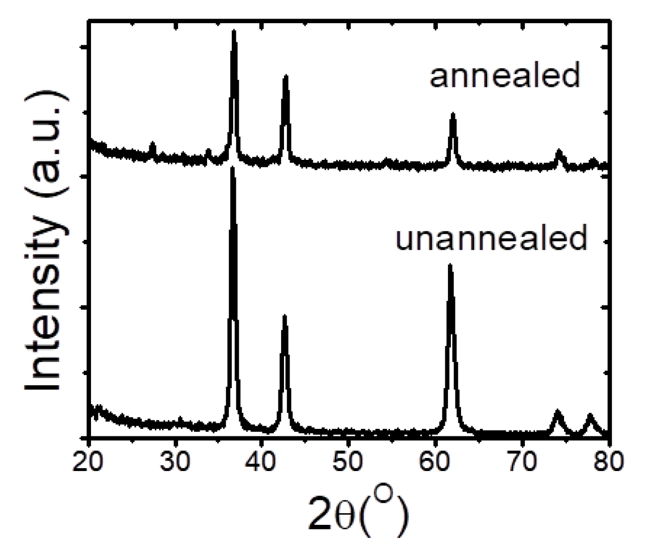
XRD was measured in the three samples (
Figure 2). The lowest curve (Sample A) is XRD of TiN grown without H
2. Samples B and C were grown with H
2, and XRD data show strong peaks in these samples. Although Ti concentration in Sample B was similar to that of Sample A, rod resistance of B was much smaller, and strong XRD peaks are shown. These data suggest that the enhanced resistance characteristics of Samples B and C are related to the H
2 added during sputtering growth. The XRD peak positions from JCPDS 38-1420 are 36.662° (111), 42.596° (200), 61.812° (220), and 74.068° (311).
XRD was measured in Sample C before and after 700 °C annealing in N
2 (
Figure 3). For this experiment, TiN film was grown on a sapphire substrate for 30 min. The purpose of this experiment was to investigate if TiN is converted to TiO
2. Although the figure shows weaker XRD peaks after the annealing, there is no significant change in the XRD characteristics. The small peak (after the annealing) at 25° is explained as (101) peak of TiO
2 anatase (25.281° from JCPDS 21-1272).
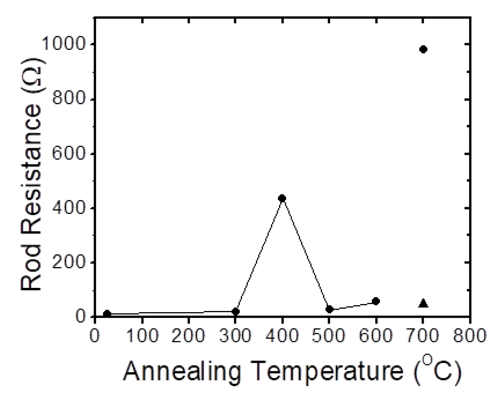
Rod resistances were measured after annealing in N
2 (
Figure 4). TiN was grown on the ceramic rods for 2 h using gas flows of Sample C in
Table 1. After growth, samples were annealed between 300 and 700 °C. The heating ramp was fixed at 120 °C/min, and cool down was done without application of any heat. After the temperature reached the target value, the temperature was sustained for 5 min. Fifteen samples were used for each temperature, and the average values of rod resistance were plotted (
Figure 4). The effect of annealing for this figure is different from that in
Figure 3, because gases trapped in the ceramic rods would react with TiN. Note that TiN in
Figure 3 was grown on a sapphire substrate, and gas contamination during annealing is much smaller.
Figure 4 shows that 400 °C annealing increased rod resistance by a large amount. In contrast, 500 and 600 °C annealing showed smaller resistance. This may be the result of reaction between Ti, N, and O.
Since the TiN film in these experiments was grown at ~100 °C, it would have excess Ti and N, as well as vacancies. During annealing, the excess atoms may undergo Ti + N or Ti + O reactions, depending on annealing conditions [
15]. At 400 °C, trapped oxygen can escape from the ceramic rods, and excess Ti can react with this oxygen, resulting in a material with higher resistance, TiO
2. At 500 and 600 °C annealing, however, it would be possible to have a Ti + N reaction in addition to the Ti + O reaction. The Ti + N reaction produces TiN, which is of lower resistance than TiO
2. At higher temperatures, it will be easier to remove the defects. This model can explain the lower resistance after annealing at 500 and 600 °C, compared to the 400 °C annealing.
For 700 °C annealing in
Figure 4, two types of temperature ramps were used. One type (circle) went up to 700 °C without any stop, and the other type (triangle) stopped at 400 °C for 9 min, before going up to 700 °C. During the 400 °C stop, N
2 gas was purged four times to remove trapped gases in the ceramic. After the normal 700 °C annealing, the rod resistance was increased to 982 Ω, which is 80 times larger than 12.3 Ω of unannealed rods. The rods with the 400 °C stop showed 48.8 Ω, which is comparable to 56.7 Ω of 600 °C annealing.
4. Discussion
These experimental results showed that the introduction of hydrogen significantly improved the quality of TiN, as indicated by a lower resistance and strong XRD peaks. The exact mechanism of hydrogen function in TiN sputtering is unclear at this moment. Increases in high-energy tail in gold sputtering [
10] and target surface conversion in metal oxide sputtering [
11] were reported. These principles can be applied to our TiN sputtering.
One possible explanation for this phenomenon may be hydrogen-induced cracking in titanium (hydrogen embrittlement). When Ti is exposed to hydrogen gas at ~300 °C, titanium hydride is formed at the surface, and Ti becomes brittle [
16]. Hydride formation is an exothermic process, and it can develop rapidly under certain conditions. For example, the presence of energetic ions during sputtering growth can accelerate hydride formation. When a Ti target has hydride on the surface, Ti emission would increase, because dissociation from the target would be easier. Another possible explanation is that lower oxygen density would decrease the mid-course reaction. The function of hydrogen in TiN deposition has not been investigated in detail. A previous study has explored the use of hydrogen in plasma spray deposition [
8], but the function of hydrogen was not discussed in detail.
The high N concentration in TiN films grown without hydrogen needs more investigation. Although EDS showed a high N/Ti ratio, it does not necessarily mean that the target was coated with nitride. The target could also be covered with a thin layer of oxide. After growth, the target color was metallic, without any irregular patterns. Detailed analysis of the target surface will be needed.


