Article

Silicon Phthalocyanines as Acceptor Candidates in Mixed Solution/Evaporation Processed Planar Heterojunction Organic Photovoltaic Devices

Department of Chemical Engineering, University of Ottawa, 161 Louis Pasteur, Ottawa, ON K1N 6N5, Canada
*
Author to whom correspondence should be addressed.
Coatings 2019, 9(3), 203; https://doi.org/10.3390/coatings9030203
Submission received: 29 January 2019 / Revised: 12 March 2019 / Accepted: 19 March 2019 / Published: 21 March 2019
(This article belongs to the Special Issue Thin Films for Electronic Applications)

Abstract

:
Silicon phthalocyanines (SiPc) are showing promise as both ternary additives and non-fullerene acceptors in organic photovoltaics (OPVs) as a result of their ease of synthesis, chemical stability and strong absorption. In this study, bis(3,4,5-trifluorophenoxy) silicon phthalocyanine ((345F)2-SiPc)) and bis(2,4,6-trifluorophenoxy) silicon phthalocyanine ((246F)2-SiPc)) are employed as acceptors in mixed solution/evaporation planar heterojunction (PHJ) devices. The donor layer, either poly(3-hexylthiophene) (P3HT) or poly[N-9′-heptadecanyl-2,7-carbazole-alt-5,5-(4′,7′-di-2-thienyl-2′,1′,3′-benzothiadiazole)] (PCDTBT), was spin coated followed by the evaporation of the SiPc acceptor thin film. Several different donor/acceptor combinations were investigated in addition to investigations to determine the effect of film thickness on device performance. Finally, the effects of annealing, prior to SiPc deposition, after SiPc deposition, and during SiPc deposition were also investigated. The devices which performed the best were obtained using PCDTBT as the donor, with a 90 nm film of (345F)2-SiPc as the acceptor, followed by thermal annealing at 150 °C for 30 min of the entire mixed solution/evaporation device. An open-circuit voltage (Voc) of 0.88 V and a fill factor (FF) of 0.52 were achieved leading to devices that outperformed corresponding fullerene-based PHJ devices.

Graphical Abstract

1. Introduction

Organic photovoltaics (OPVs) have been of major interest over the past years as a potentially lightweight, flexible, and semi-transparent renewable energy source. Indeed, solar energy holds great potential [1,2], and inexpensive processing of OPVs can lead to a shorter energy payback compared to inorganic silicon cells [3,4,5]. The most common OPV device configuration is a bulk heterojunction (BHJ), which is based on a random network of electron donating semiconductive polymers and electron accepting small molecules [3]. The most studied donor/acceptor pair is P3HT (poly[3-hexylthiophene]) and PC61BM (phenyl-C61-butyric acid methyl ester) resulting in baseline power conversion efficiencies (PCEs) ranging from 2% to 5% [6]. Recently, BHJ OPV devices have reached high PCEs (sometimes above 15%) when employing small band gap polymers and non-fullerene acceptors (NFAs) [7,8,9,10]. In a BHJ, the active layer is a kinetically trapped blend of acceptor and donor materials that, with time and heat, will undergo a detrimental phase separation [11,12]. Secondly, the active layer blend morphology is a function of the processing conditions and will therefore depend on factors such as shearing speed and drying time, thus presenting significant challenges in transitioning from lab-scale device fabrication to scale-up and commercialization. The use of a planar heterojunction (PHJ), where the donor/acceptor bilayer is formed through successive physical vapor depositions, can lead to more interesting morphologies by engineering greater charge percolation to the respective electrodes followed by a simpler development through independent thickness optimization (as compared to blend engineering for BHJ). PHJ devices can also be fabricated through sequential depositions of solutions, in a structure known as a diffuse planar heterojunction (DPHJ) OPV, as a result of the second solution swelling or diffusing into the first layer, producing a mixed or blended interface [13,14]. In the literature, DPHJ devices have achieved similar PCEs compared to BHJ devices, with values exceeding 3.5% using fullerene derivatives [12,15]. Poly[N-9′-heptadecanyl-2,7-carbazole-alt-5,5-(4′,7′-di-2-thienyl-2′,1′,3′-benzothiadiazole)] (PCDTBT), is a well-studied donor polymer which outperforms P3HT-based BHJ when paired with PC61BM and PC71BM resulting in PCEs of >7% [16,17,18], with long-term stability [19]. However, to the best of our knowledge, only one application of DPHJ devices with PC71BM has been reported using PCDTBT [20]. Only a few studies have explored the combination of a solution processed layer followed by the evaporation of C60 resulting in a hybrid processed bilayer device [21,22]. Despite their good accepting abilities and their high electron mobility, fullerene derivatives only have a small absorption overlap with the solar spectrum, and their relatively small band gap limits the resulting device open-circuit voltage (Voc), which is directly related to the energy difference between the donor highest occupied molecular orbital (HOMO) and the acceptor lowest unoccupied molecular orbital (LUMO) [23,24,25]. Secondly, the synthesis of fullerene derivatives is very energy demanding because of the numerous low yielding steps and non-effective purification procedures [26,27].
Metal containing phthalocyanines (MPcs) are planar aromatic macrocycles consisting of four linked isoindoline units bound to a central metal atom. They have been used widely as dyes and pigments in industry due to their general chemical stability and low production cost [28,29,30]. MPcs are also employed in organic electronic applications as the semiconductor. Their high molar extinction coefficient (in the order of 105 M−1·cm−1) [31,32] and their relatively high charge transport properties (mobilities in the order of 10−5 up to 2.5 cm2·V−1·s−1), due to favorable molecular stacking, have facilitated their application in organic thin film transistors (OTFTs) [33,34,35,36,37], organic light emitting diode (OLEDs) [38,39,40,41], and OPVs [42,43,44,45,46]. Even if divalent MPcs such as zinc MPc (ZnPc) or copper MPc (CuPc) are well studied, the use of tetravalent MPcs such as tin MPcs (SnPc) or silicon MPcs (SiPc) remain limited [35,47].
Recently, SiPcs have attracted significant interest from our group and others for their integration into OPVs, both as an additive in BHJ devices [48,49,50,51] or as an acceptor or donor in either BHJ or PHJ devices [52,53,54]. We reported the use of bis(6-azidohexanoate)silicon phthalocyanine ((HxN3)2-SiPc) as the first dual function ternary additive for OPV, which improved the device stability through cross linking while simultaneously increasing the PCE by absorbing in the near IR region [49]. Through axial substitution such as phenoxylation, it is also possible to engineer the solid state stacking of the resulting SiPc derivatives in the thin films. Lessard et al. fabricated a series of thermally evaporated PHJ OPV devices using SiPc as both the donor materials when paired with fullerene (C60), and as acceptor materials when paired with pentacene or α-sexithiophene (α-6T). In all device configurations, as a result of favorable solid state arrangement, bis(pentafluorophenoxy) SiPc (F10-SiPc) resulted in devices with a 3-fold increase of both Voc and short circuit current (Jsc) compared to dichloro SiPc (Cl2-SiPc)-based devices [52]. Following this study, the researchers explored synthetizing different SiPcs with distinct frequencies and positions of the fluoro atoms, as this would change the material properties and arrangement and the resulting device performance. Bis(3,4,5-trifluorophenoxy) SiPc ((345F)2-SiPc) and bis(2,4,6-trifluorophenoxy) SiPc ((246F)2-SiPc) were determined to further outperform F10-SiPc, with a Voc as high as 0.87 V and a PCE as much as 1.8% [53]. These performances are quite promising for unoptimized devices that are already outperforming other PHJ devices based on well-studied phthalocyanines such as chloro aluminum MPc (Cl-AlPc) [43,46,55,56,57] or CuPc [43,58,59,60], further justifying the exploration of SiPcs as thermally evaporated NFAs.
In this study, we aim to combine the benefits of using conjugated polymers as the donor layer while incorporating SiPcs as the acceptor layer through thermal evaporation in a mixed solution/evaporation PHJ device structure. Both P3HT and PCDTBT were used as the polymer donor layer, while (246F)2-SiPc and (345F)2-SiPc were used as the evaporated acceptor layer. We also report the effect of the frontier orbital energy levels of the materials, the film thickness, and the results of the thermal treatment.

2. Materials and Methods

2.1. Materials

o-Dichlorobenzene (o-DCB, >99%) was purchased from Sigma-Aldrich (St. Louis, MO, USA). Poly(3,4-ethylenedioxythiophene) poly(styrene sulfonate) (PEDOT:PSS, CleviosTM HTL Solar) was purchased from Heraeus (Hanau, Germany). PCDTBT (Lot#SX7283CH, Mw 40k) was acquired from 1-Material (Dorval, QC, Canada) and P3HT (Lot# PTL24-94, RR 93%, Mw 83K) was purchased from Rieke Metals (Lincoln, Nebraska). The fullerene (6,6)-phenyl-C61-butyric acid metyl ester (PC61BM) was purchased from Nano-C (Westwood, MA, USA). Bathocuprione (BCP, >99%) and silver (Ag) were purchased from Lumtec (New Taipei City, Taiwan) and Angstrom Engineering (Kitchener, ON, Canada), respectively. All materials were used as received unless otherwise specified. Bis(3,4,5-trifluorophenoxy) silicon phthalocyanine ((345F)2-SiPc) and bis(2,4,6-trifluorophenoxy) silicon phthalocyanine ((246F)2-SiPc) were synthetized and purified according to the literature [53].

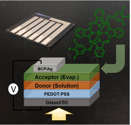
2.2. Device Fabrication

Bilayer devices were made by first dissolving P3HT (15 mg/mL) or PCDTBT (8 mg/mL) in o-DCB and were stirred overnight at 50 °C. Substrates of glass coated with indium tin oxide (ITO) were cleaned by subsequent sonication of 5 min in detergent, deionized water, acetone, and methanol, followed by an air-plasma treatment for 10 min. PEDOT:PSS was spin-coated onto the ITO at 3000 rpm for 30 s, and dried in a vacuum oven for 15 min at 140 °C. The donor polymer layer was then spin-coated on top of the PEDOT:PSS layer at 2000 rpm for 60 s under a nitrogen atmosphere and allowed to dry for at least 2 h at room temperature. The silicon phthalocyanine (SiPc) acceptor layer, BCP (9 nm) and Ag (70 nm) were thermally evaporated onto the polymer layer in a custom Angstrom Engineering vacuum chamber system built into a glove box (base pressure = 1 × 10⁻⁷ Torr). A shadow mask was used for the evaporation of BCP/Ag for defining the device electrodes, providing five 0.325 cm2 devices per glass substrate. The resulting devices had the following structure: glass/ITO/PEDOT:PSS/donor layer/acceptor layer/BCP/Ag. For some sets of devices, annealing was performed in a vacuum oven. The PCDTBT layer was annealed before the evaporation of the SiPc layer at 150 °C for 10, 30, and 60 min. Other devices were also annealed during the evaporation of the SiPc layer at 150 °C using an in situ substrate heater, and after the SiPc evaporation but before the deposition of the BCP and Ag at 150 °C for 30 min.

2.3. Device Characterization

Current density vs. voltage curves were measured under nitrogen atmosphere using simulated solar light supplied by a Xenon arc lamp (Abet Technologies, Milford, CT, USA) with an Air Mass 1.5 Global filter, with a Keithley 2401 Low Voltage source meter. The solar simulator was calibrated with a silicon reference cell (Abet 15150) to 1000 W/m2. Devices were mounted on an opaque holder, which eliminated diffuse light. Thicknesses were assessed using a Brucker Dektak XT Profilometer (Billerica, MA, USA). Small samples areas were scratched using a tweezer tip and then wiped with acetone to fully remove the layers. An average of 20 measurements were taken for each sample at different locations on the substrate.

3. Results and Discussion

3.1. Determination of the Acceptor/Donor Couple

Mixed solution/evaporation planar heterojunction (PHJ) OPV devices were fabricated by spincoating either P3HT or PCDTBT onto a PEDOT:PSS layer followed by the thermal evaporation of bis(3,4,5-trifluorophenoxy) silicon phthalocyanine ((345F)2-SiPc) or bis(2,4,6-trifluorophenoxy) silicon phthalocyanine ((246F)2-SiPc) with the structure glass/ITO/PEDOT:PSS/P3HT or PCDTBT/(246F)2-SiPc or (345F)2-SiPc /BCP/Ag represented in Figure 1. More than 80 P3HT:PC61BM bulk heterojunction (BHJ) OPV baseline devices were also fabricated in parallel to exclude sporadic fabrication errors. All devices were characterized and the corresponding short circuit current (Jsc), open circuit voltage (Voc), and fill factor (FF) are presented in Table 1. P3HT:PC61BM BHJ OPV baseline devices performed according to literature [6] with a Jsc = 8.19 ± 0.43 mA∙cm−2, Voc = 0.56 ± 0.02 V and FF = 0.61 ± 0.04 resulting in an average power conversion efficiency (PCE) of 2.87% ± 0.21%. Our P3HT/C60 PHJ OPV baseline devices also performed according to literature [21] with a Jsc = 2.58 ± 0.05 mA∙cm−2, Voc = 0.22 ± 0.01 V, FF = 0.48 ± 0.02, and PCE = 0.28 ± 0.02%. It should be noted that our devices have an area of 0.325 cm2, which is larger than other commonly reported devices in literature.
Initially we paired (345F)2-SiPc with P3HT in our PHJ OPV devices. The P3HT thickness was kept constant while the (345F)2-SiPc thickness was varied between 10 and 60 nm. Figure 2a demonstrates the JV curves for the resulting bilayer devices while Figure 2b plots the average Jsc and Voc evolution as a function of (345F)2-SiPc thickness. As the thickness increases from 10 to 60 nm, both the Jsc and Voc values increase, reaching a maximum value of 1.09 ± 0.06 mA∙cm−2 and 0.34 ± 0.03 V, respectively (Table 1). The increase in Jsc with increasing thickness of SiPc is likely caused by the increase in light absorption and exciton generation. The increase in Voc with the increase in SiPc thickness might be due to the enhancement of polaron-pair bounding energy (EB), which indicates that a higher polaron-pair dissociation energy barrier has to be overcome, and that a higher applied voltage is required to fully dissociate the accumulated excitons near the polymer/SiPc interface. [61,62,63] As a result, higher Voc is essential. Compared to the P3HT/C60 baseline devices, when using (345F)2-SiPc, a greater Voc was obtained, however the Jsc appears to be substantially reduced which led to the limited performances of the devices. These results illustrate that tuning the thickness of (345F)2-SiPc is a straight-forward way to optimize the PHJ OPV device performance.
In attempts to increase the Voc, (345F)2-SiPc was substituted with (246F)2-SiPc which has been characterized to have a shallower (≈0.5 eV) LUMO energy level [53]. This increase in LUMO level will lead to a bigger energy difference with the P3HT HOMO, which is known to raise the resulting Voc [25]. Figure 2c demonstrates the performance for P3HT/(246F)2-SiPc in terms of averaged Jsc and Voc evolution according to the SiPc thickness. An improvement of 0.2 V for Voc is observed for 40 nm (246F)2-SiPc compared to devices with the same (345F)2-SiPc thickness with a maximum Voc of 0.49 ± 0.02 V (Table 1, Figure 2a). When comparing the corresponding bilayer devices, P3HT/(246F)2-SiPc has a greater Voc than P3HT/C60 baseline devices. In addition, when comparing the BHJ equivalent, P3HT: bis(tri-n-butylsilyl oxide) silicon phthalocyanine ((3BS)2-SiPc) has a greater Voc than P3HT:PC61BM [45]. Therefore, the fact that the baseline P3HT:PC61BM BHJ OPV has a greater Voc than bilayer P3HT/(246F)2-SiPc shows that it must be a function of device structure and not a function of the HOMO/LUMO levels of the SiPc materials. However, it is clear that the use of (246F)2-SiPc also results in a significant drop in Jsc compared to the use of (345)2-SiPc, which was 0.6 ± 0.06 mA∙cm−2, as shown in Figure 2c,d. As the thickness of (246F)2-SiPc is increased to 60 nm we observe a drop in Jsc which is likely due to the greater series resistance related to the relatively low electron mobility of SiPcs [37].
In an attempt to increase the energy difference between the donor HOMO and the SiPc acceptor LUMO, P3HT was replaced with PCDTBT, leading to a decrease in the donor HOMO from −5.0 eV for P3HT to −5.5 eV for PCDTBT [18]. For this first set of experiments, the (345F)2-SiPc thickness was kept constant at 60 nm, while the PCDTBT thickness was varied by changing the spin coating rate. Figure 2e,f demonstrates the performance for PCDTBT/(345F)2-SiPc PHJ OPV devices in terms of averaged Jsc and Voc as a function of the PCDTBT spin coating rate, and their corresponding JV curves. These experiments show very little variations in results between 1000 and 3000 rpm. However, compared to P3HT/(345F)2-SiPc, these devices demonstrated an improvement of 132% and 186% in both the Voc and Jsc, respectively. The optimum devices were characterized by a Jsc = 3.15 ± 0.04 mA∙cm−2 and a Voc of 0.79 ± 0.06 V, outperforming the PCDTBT/C60 baseline in Table 1. PHJ OPV devices were fabricated using (246F)2-SiPc on the PCDTBT and as expected a very poor device performance was obtained (Table 1). This drop in performance is a result of the mismatch of HOMO/LUMO levels of PCDTBT and (246F)2-SiPc.

3.2. (345F)2-SiPc Thickness Improvement

The effect of the (345F)2-SiPc thickness on the PCDTBT-based PHJ OPV device performances was assessed. The (345F)2-SiPc thickness was varied between 20 and 120 nm and its effect on the corresponding device performance was plotted for the Voc (Figure 3a), Jsc (Figure 3b), FF (Figure 3c), and PCE (Figure 3d). We found that consistent and optimal PHJ OPV device performances were obtained with (345F)2-SiPc films of thickness 60–105 nm. For thicknesses <60 nm and >105 nm, performances dropped significantly (Figure 3). The best results were obtained for a (345F)2-SiPc thickness of roughly 90 nm characterized by a Voc of 0.87 ± 0.03 V, a Jsc of 3.32 ± 0.04 mA∙cm−2, a FF of 0.37 ± 0.01, and a PCE of 1.05% ± 0.04%. Compared to PCDTBT/C60 baselines, the use of SiPc resulted in superior Voc but lower Jsc and FF values, which led to a reduced PCE. Therefore, a series of thermal treatments were explored to attempt to enhance the device performance.

3.3. Thermal Treatment

3.1.1. Annealing before the Evaporation of (345F)2-SiPc

Reports have shown that the ordering of the PCDTBT layer by thermal annealing or through the addition of an ordering agent can help prevent degradation during the deposition of the subsequent layer [20]. Therefore, after PCDTBT was spin coated, it was placed in an oven at 150 °C for 10, 30, and 60 min. The polymer film was removed from the oven and the (345F)2-SiPc layer was evaporated on all the films. Figure S1a shows the evolution of the device JV curves with increasing anneal time. The greatest Voc = 0.74 ± 0.08 V and Jsc = 3.34 ± 0.08 mA∙cm−2 were obtained for devices that underwent no annealing. The longer the annealing, the worse the devices became. Secondly, we explored the use of an ordering agent, such as 1,8-diiodooctane (DIO) as reported in Reference [20], in the PCDTBT layer. Figure S2a shows the impact on the JV curves with the addition of different DIO concentrations in the PCDTBT layer followed by the subsequent evaporation of a 113 nm thick (345F)2-SiPc. The baseline containing no DIO displays a poor JV curve with a low FF, Voc, and Jsc equal to 0.29, 0.43 V, and 2.6 mA∙cm−2, respectively. The addition of 1 vol % of DIO in the o-DCB led to a great improvement in the Voc to around 0.7 V while the Jsc remained similar, and the addition of 3 vol % DIO helped increase the Voc a bit more to above 0.8 V whilst also improving the FF to 0.37. Figure S2b shows the impact on the JV curves of an addition of 3 vol % DIO in the PCDTBT layer, also followed by a thermal annealing at 100 °C for 15 min, followed by the deposition of 104 nm of (345F)2-SiPc. The addition of DIO alone led to a drastic decrease in both Voc and Jsc of roughly 0.2 V and 0.5 mA∙cm−2, respectively. The annealing step after the PCDTBT spin coating appeared to counteract the DIO effect, but the values still show an underperformance as compared to the baseline devices. Figure S2c shows the previous result for a (345F)2-SiPc thickness of 65 nm. Again, the addition of DIO still has a negative impact, decreasing the resulting Voc. Performing the annealing step again raises the Voc value and improves the FF, but by no more than would be the case after omitting the DIO altogether. Overall, these results indicate that thermal treatment and the use of DIO did not offer any advantage.

3.1.2. Annealing after the (345F)2-SiPc Evaporation

We explored the annealing of the PCDTBT/(345F)2-SiPc bilayer (in a vacuum oven at 150 °C for 30 min) prior to the deposition of the BCP/Ag layers. Results for these devices are shown in Table 1 and Figure 4. The application of the annealing step (post (345F)2-SiPc deposition) led to a significant gain in performances for PCDTBT/(345F)2-SiPc (93nm) devices due to the improvement in Jsc to 3.44 ± 0.18 mA∙cm−2 and the significant increase of the FF to 0.51 ± 0.02. The final PCE of the PCDTBT/(345F)2-SiPc resulted in a superior PCE increase from 0.97% ± 0.06% to 1.52% ± 0.06%, slightly surpassing the PCDTBT/C60 PHJ OPV devices that showed a PCE of 1.48% ± 0.06%. These results suggest that straightforward annealing can improve SiPc-based PHJ OPV devices.

3.1.3. Annealing during the (345F)2-SiPc Evaporation

It is well known that an increased surface area between the acceptor and the donor will result in improved exciton dissociation which can lead to a raised PCE [64]. Therefore, a fuzzy or blended interface could result in better device performance. For this set of devices during the fabrication of the PCDTBT/(345F)2-SiPc interface, we heated the substrates to 150 °C under vacuum during the SiPc evaporation. The hypothesis was that a higher surface energy (or softening of the PCDTBT) during the deposition would facilitate the penetration of the SiPc molecule deeper into the PCDTBT layer resulting in a fuzzy interface. As the PHJ annealing after the SiPc deposition seemed beneficial, it was also performed on devices before the deposition of the last BCP/Ag layers in a vacuum oven at 150 °C for 0, 5, 15, and 30 min.
Figure 5 shows the evolution of the average Voc (Figure 5a), Jsc (Figure 5b), FF (Figure 5c), and PCE (Figure 5d) as a function of the variation of post annealing time after the heated SiPc deposition. For devices that were only heated during the evaporation (time = 0 min), the performances were well below what was achieved previously with Voc < 0.1 V, the Jsc ≈ 1.5 mA∙cm−2, the FF ≈ 0.26, and the PCE ≈ 0.03%. The addition of the PHJ annealing step after the evaporation helped increase these parameters, the best device being achieved after 15 min annealing with a Voc, Jsc, FF, and PCE of 0.47 ± 0.09 V, 2.6 ± 0.23 mA∙cm−2, 0.34% ± 0.02%, and 0.43% ± 0.12%, respectively. These results suggest that heating during the deposition of the (345F)2-SiPc is not an effective route towards improved device performance.

4. Conclusions

A series of PHJ OPV mixed solution/evaporation devices were fabricated using (246F)2-SiPc or (345F)2-SiPc as the acceptor material, which were evaporated on either P3HT or PCDTBT as the solution processed donor layer. The devices were optimized through the substitution of materials and through controlling the acceptor thickness. We found that the spin rate of the PCDTBT had little effect on the device performance while the thickness of SiPc played a critical role. The optimal SiPc thickness was found to be roughly 90 nm. In attempts to improve these devices, a series of thermal treatments were applied to the most promising PCDTBT/(345F)2-SiPc devices. Annealing of the PCDTBT layer alone, prior to (345F)2-SiPc deposition with and without the addition of a small volume percentage of DIO, resulted in no significant improvement. However, annealing of the PHJ after (345F)2-SiPc deposition, but before the BCP and Ag evaporation, led to increased FF = 0.51 ± 0.02 outperforming the PCDTBT/C60 baseline PHJ devices with a PCE of 1.52 ± 0.06%. These devices also surpassed previously reported all-evaporated PHJ devices based on (246F)2-SiPc and (345F)2-SiPc as NFAs when using α-sexithiophene as the donor layer [53]. Therefore, this study further justifies the continued investigation into using SiPcs as acceptor candidates in fullerene free devices.

Supplementary Materials

The following are available online at https://www.mdpi.com/2079-6412/9/3/203/s1, Figure S1: Characteristic current vs. voltage (J-V) for PHJ OPV devices where the active layer is PCDTBT/(345F)2-SiPc (50 nm) and where the PCDTBT layer have been annealed at 150 °C for 0, 10, 30 and 60 min; Figure 2: Characteristic current vs. voltage (J-V) for PHJ PCDTBT/(345F)2-SiPc devices with a SiPc thickness of (a) 113nm with incorporated DIO in the PCDTBT layer at 0, 1 and 3 vol %, (b) 104 nm and (c) 65 nm where DIO have been incorporated in the PCDTBT layer at 0, 3 and 3 vol % followed by annealing at 100 °C for 15 min.

Author Contributions

Conceptualization, M.D.M.F. and B.H.L.; Methodology, M.D.M.F. and B.H.L.; Validation, M.D.M.F.; Formal Analysis, M.D.M.F.; Investigation, M.D.M.F.; Resources, B.H.L.; Data Curation, M.D.M.F.; Writing—Original Draft Preparation, M.D.M.F.; Writing—Review and Editing, M.D.M.F., B.H.L, and T.M.G.; Visualization, M.D.M.F.; Supervision, B.H.L.; Project Administration, B.H.L.; Funding Acquisition, B.H.L.

Funding

This research was funded by Natural Sciences and Engineering Research Council (NSERC) SPG-P to B.H.L. Ontario Graduate Scholarship (OGS) to T.M.G. Infrastructure used to complete this work was acquired using CFI-JELF and NSERC RTI.

Acknowledgments

We would like to thank Steven Xiao from 1-material for the in-kind contribution of PCDTBT.

Conflicts of Interest

The authors declare no conflict of interest.

References

  1. Battaglia, C.; Cuevas, A.; De Wolf, S. High-efficiency crystalline silicon solar cells: status and perspectives. Energy Environ. Sci. 2016, 9, 1552–1576. [Google Scholar] [CrossRef] [Green Version]
  2. Lee, M.M.; Teuscher, J.; Miyasaka, T.; Murakami, T.N.; Snaith, H.J. Efficient hybrid solar cells based on meso-superstructured organometal halide perovskites. Science 2012, 338, 643–648. [Google Scholar] [CrossRef] [PubMed]
  3. Hoppe, H.; Sariciftci, N.S. Organic solar cells: An overview. J. Mater. Res. 2004, 19, 1924–1945. [Google Scholar] [CrossRef]
  4. Forrest, S.R. The path to ubiquitous and low-cost organic electronic appliances on plastic. Nature 2004, 428, 911–918. [Google Scholar] [CrossRef] [PubMed]
  5. Nørgaard, L.H.; Andreasen, J.B.; Marquard, M.; Debois, S.; Larsen, F.S.; Jeppesen, V. Declarative process models in government centric case and document management. In Proceedings of the BPM 2017 Industry Track, Barcelona, Spain, 10–15 September 2017. [Google Scholar]
  6. Dang, M.T.; Hirsch, L.; Wantz, G. P3HT:PCBM, best seller in polymer photovoltaic research. Adv. Mater. 2011, 23, 3597–3602. [Google Scholar] [CrossRef] [PubMed]
  7. Yuan, J.; Zhang, Y.; Yuan, J.; Zhang, Y.; Zhou, L.; Zhang, G.; Yip, H.; Lau, T.; Lu, X. Single-junction organic solar cell with over 15% efficiency using fused-ring acceptor with electron-deficient core single-junction organic solar cell with over 15% efficiency using fused-ring acceptor with electron-deficient core. Joule 2019. [Google Scholar] [CrossRef]
  8. Yan, C.; Barlow, S.; Wang, Z.; Yan, H.; Jen, A.K.Y.; Marder, S.R.; Zhan, X. Non-fullerene acceptors for organic solar cells. Nat. Rev. Mater. 2018, 3, 18003. [Google Scholar] [CrossRef]
  9. Wang, C.; Jiang, B.H.; Su, Y.W.; Jeng, R.J.; Wang, Y.J.; Chen, C.P.; Wong, K.T. Si-bridged ladder-type small-molecule acceptors for high-performance organic photovoltaics. ACS Appl. Mater. Interfaces 2018, 11, 1125–1134. [Google Scholar] [CrossRef]
  10. Yu, Y.; Tsai, T.; Chen, C. Efficient ternary organic photovoltaics using two conjugated polymers and a nonfullerene acceptor with complementary absorption and cascade energy-level alignment. J. Phys. Chem. C 2018, 122, 24585–24591. [Google Scholar] [CrossRef]
  11. Schaffer, C.J.; Palumbiny, C.M.; Niedermeier, M.A.; Jendrzejewski, C.; Santoro, G.; Roth, S.V.; Mller-Buschbaum, P. A direct evidence of morphological degradation on a nanometer scale in polymer solar cells. Adv. Mater. 2013, 25, 6760–6764. [Google Scholar] [CrossRef] [PubMed]
  12. Ayzner, A.L.; Tassone, C.J.; Tolbert, S.H.; Schwartz, B.J. Reappraising the need for bulk heterojunctions in polymer-fullerene photovoltaics: The role of carrier transport in all-solution-processed P3HT/PCBM bilayer solar cells. J. Phys. Chem. C 2009, 113, 20050–20060. [Google Scholar] [CrossRef]
  13. Lee, K.H.; Schwenn, P.E.; Smith, A.R.G.; Cavaye, H.; Shaw, P.E.; James, M.; Krueger, K.B.; Gentle, I.R.; Meredith, P.; Burn, P.L. Morphology of all-solution-processed “bilayer” organic solar cells. Adv. Mater. 2011, 23, 766–770. [Google Scholar] [CrossRef] [PubMed]
  14. Vohra, V.; Arrighetti, G.; Barba, L.; Higashimine, K.; Porzio, W.; Murata, H. Enhanced vertical concentration gradient in rubbed P3HT:PCBM graded bilayer solar cells. J. Phys. Chem. Lett. 2012, 3, 1820–1823. [Google Scholar] [CrossRef] [PubMed]
  15. Moon, J.S.; Takacs, C.J.; Sun, Y.; Heeger, A.J. Spontaneous formation of bulk heterojunction nanostructures: Multiple routes to equivalent morphologies. Nano Lett. 2011, 11, 1036–1039. [Google Scholar] [CrossRef]
  16. Gholamkhass, B.; Servati, P. Solvent-vapor induced morphology reconstruction for efficient PCDTBT based polymer solar cells. Org. Electron. Phys. Mater. Appl. 2013, 14, 2278–2283. [Google Scholar] [CrossRef]
  17. Wakim, S.; Beaupré, S.; Blouin, N.; Aich, B.; Rodman, S.; Gaudiana, R.; Tao, Y.; Leclerc, M. Highly efficient organic solar cells based on a poly(2,7-carbazole) derivative. J. Mater. Chem. 2009, 19, 5351–5358. [Google Scholar] [CrossRef]
  18. Park, S.H.; Roy, A.; Beaupré, S.; Cho, S.; Coates, N.; Moon, J.S.; Moses, D.; Leclerc, M.; Lee, K.; Heeger, A.J. Bulk heterojunction solar cells with internal quantum efficiency approaching 100%. Nat. Photonics 2009, 3, 297–303. [Google Scholar] [CrossRef]
  19. Wang, D.H.; Kim, J.K.; Seo, J.H.; Park, O.O.; Park, J.H. Stability comparison: A PCDTBT/PC 71BM bulk-heterojunction versus a P3HT/PC 71BM bulk-heterojunction. Sol. Energy Mater. Sol. Cells 2012, 101, 249–255. [Google Scholar] [CrossRef]
  20. Seok, J.; Shin, T.J.; Park, S.; Cho, C.; Lee, J.Y.; Ryu, D.Y.; Kim, M.H.; Kim, K. Efficient Organic Photovoltaics Utilizing Nanoscale Heterojunctions in Sequentially Deposited Polymer/fullerene Bilayer. Sci. Rep. 2015, 5, 8373. [Google Scholar] [CrossRef] [Green Version]
  21. Josey, D.S.; Castrucci, J.S.; Dang, J.D.; Lessard, B.H.; Bender, T.P. Evaluating thiophene electron-donor layers for the rapid assessment of boron subphthalocyanines as electron acceptors in organic photovoltaics: Solution or vacuum deposition? ChemPhysChem 2015, 16, 1245–1250. [Google Scholar] [CrossRef]
  22. Yang, Y.; Aryal, M.; Mielczarek, K.; Hu, W.; Zakhidov, A. Nanoimprinted P3HT/C60 solar cells optimized by oblique deposition of C60. J. Vac. Sci. Technol. B 2010, 28, C6M104–C6M107. [Google Scholar]
  23. Li, C.Z.; Yip, H.L.; Jen, A.K.Y. Functional fullerenes for organic photovoltaics. J. Mater. Chem. 2012, 22, 4161–4177. [Google Scholar] [CrossRef]
  24. Hoke, E.T.; Vandewal, K.; Bartelt, J.A.; Mateker, W.R.; Douglas, J.D.; Noriega, R.; Graham, K.R.; Fréchet, J.M.J.; Salleo, A.; McGehee, M.D. Recombination in polymer:Fullerene solar cells with open-circuit voltages approaching and exceeding 1.0 V. Adv. Energy Mater. 2013, 3, 220–230. [Google Scholar] [CrossRef]
  25. Kooistra, F.B.; Knol, J.; Kastenberg, F.; Popescu, L.M.; Verhees, W.J.H.; Kroon, J.M.; Hummelen, J.C. Increasing the open circuit voltage of bulk-heterojunction solar cells by raising the LUMO level of the acceptor. Org. Lett. 2007, 9, 551–554. [Google Scholar] [CrossRef]
  26. Anctil, A.; Babbitt, C.W.; Raffaelle, R.P.; Landi, B.J. Material and energy intensity of fullerene production. Environ. Sci. Technol. 2011, 45, 2353–2359. [Google Scholar] [CrossRef]
  27. Anctil, A.; Babbitt, C.W.; Raffaelle, R.P.; Landi, B.J. Cumulative energy demand for small molecule and polymer photovoltaics. Prog. Photovol. Res. Appl. 2013, 21, 1541–1554. [Google Scholar] [CrossRef]
  28. Allen, C.G.; Martin, I.; Gordon, K. Hydroxygallium phthalocyanine pigments with block copolymer binders. U.S. Patent 5521043, 28 May 1996. [Google Scholar]
  29. Giambalvo, V.A.; Lee, W.; Cyan, A. Non-crystallizing, non-flocculating phthalocyanines. U.S. Patent 3589924, 29 June 1971. [Google Scholar]
  30. De La Torre, G.; Claessens, C.G.; Torres, T. Phthalocyanines: Old dyes, new materials. Putting color in nanotechnology. Chem. Commun. 2007, 20, 2000–2015. [Google Scholar] [CrossRef]
  31. Lim, B.; Margulis, G.Y.; Yum, J.; Unger, E.L.; Hardin, B.E.; Gr, M.; Mcgehee, M.D.; Sellinger, A. Silicon-naphthalo/phthalocyanine-hybrid sensitizer for efficient red response in dye-sensitized solar cells. Org. Lett. 2013, 15, 2011–2014. [Google Scholar] [CrossRef]
  32. El-nahass, M.M.; El-gohary, Z.; Soliman, H.S. Structural and optical studies of thermally evaporated CoPc thin films. Opt. Laser Technol. 2003, 35, 523–531. [Google Scholar] [CrossRef]
  33. Roberts, M.E.; Sokolov, A.N.; Bao, Z. Material and device considerations for organic thin-film transistor sensors. J. Mater. Chem. 2009, 19, 3351–3363. [Google Scholar] [CrossRef]
  34. Li, X.; Jiang, Y.; Xie, G.; Tai, H.; Sun, P.; Zhang, B. Copper phthalocyanine thin film transistors for hydrogen sulfide detection. Sens. Actuators B Chem. 2013, 176, 1191–1196. [Google Scholar] [CrossRef]
  35. Melville, O.A.; Lessard, B.H.; Bender, T.P. Phthalocyanine-based organic thin-film transistors: A review of recent advances. ACS Appl. Mater. Interfaces 2015, 7, 13105–13118. [Google Scholar] [CrossRef]
  36. Boileau, N.T.; Melville, O.A.; Mirka, B.; Cranston, R.; Lessard, B.H. P and N type copper phthalocyanines as effective semiconductors in organic thin-film transistor based DNA biosensors at elevated temperatures. RSC Adv. 2019, 9, 2133–2142. [Google Scholar] [CrossRef]
  37. Melville, O.A.; Grant, T.M.; Lessard, B.H. Silicon phthalocyanines as N-type semiconductors in organic thin film transistors. J. Mater. Chem. C 2018, 6, 5482–5488. [Google Scholar] [CrossRef]
  38. Deng, Z.; Lü, Z.; Chen, Y.; Yin, Y.; Zou, Y.; Xiao, J.; Wang, Y. Aluminum phthalocyanine chloride as a hole injection enhancer in organic light-emitting diodes. Solid-State Electron. 2013, 89, 22–25. [Google Scholar] [CrossRef]
  39. Lessard, B.H.; Sampson, K.L.; Plint, T.; Bender, T.P. Boron subphthalocyanine polymers: Avoiding the small molecule side product and exploring their use in organic light-emitting diodes. J. Polym. Sci. Part A Polym. Chem. 2015, 53, 1996–2006. [Google Scholar] [CrossRef]
  40. Pearson, A.J.; Plint, T.; Jones, S.T.; Lessard, B.H.; Credgington, D.; Bender, T.P.; Greenham, N.C. Silicon phthalocyanines as dopant red emitters for efficient solution processed OLEDs. J. Mater. Chem. C 2017, 5, 12688–12698. [Google Scholar] [CrossRef]
  41. Plint, T.; Lessard, B.H.; Bender, T.P. Assessing the potential of group 13 and 14 metal/metalloid phthalocyanines as hole transport layers in organic light emitting diodes. J. Appl. Phys. 2016, 119, 145502. [Google Scholar] [CrossRef]
  42. Xue, J.; Uchida, S.; Rand, B.P.; Forrest, S.R. Asymmetric tandem organic photovoltaic cells with hybrid planar-mixed molecular heterojunctions. Appl. Phys. Lett. 2004, 85, 5757–5759. [Google Scholar] [CrossRef]
  43. Kim, D.Y.; So, F.; Gao, Y. Aluminum phthalocyanine chloride/C60 organic photovoltaic cells with high open-circuit voltages. Sol. Energy Mater. Sol. Cells 2009, 93, 1688–1691. [Google Scholar] [CrossRef]
  44. Cnops, K.; Rand, B.P.; Cheyns, D.; Verreet, B.; Empl, M.A.; Heremans, P. 8.4% efficient fullerene-free organic solar cells exploiting long-range exciton energy transfer. Nat. Commun. 2014, 5, 3406. [Google Scholar] [CrossRef] [PubMed]
  45. Dang, M.T.; Grant, T.M.; Yan, H.; Seferos, D.S.; Lessard, B.H.; Bender, T.P. Bis(tri-n-alkylsilyl oxide) silicon phthalocyanines: A start to establishing a structure property relationship as both ternary additives and non-fullerene electron acceptors in bulk heterojunction organic photovoltaic devices. J. Mater. Chem. A 2017, 5, 12168–12182. [Google Scholar] [CrossRef]
  46. Yuen, A.P.; Jovanovic, S.M.; Hor, A.M.; Klenkler, R.A.; Devenyi, G.A.; Loutfy, R.O.; Preston, J.S. Photovoltaic properties of M-phthalocyanine/fullerene organic solar cells. Sol. Energy 2012, 86, 1683–1688. [Google Scholar] [CrossRef]
  47. Williams, G.; Sutty, S.; Klenkler, R.; Aziz, H. Renewed interest in metal phthalocyanine donors for small molecule organic solar cells. Sol. Energy Mater. Sol. Cells 2014, 124, 217–226. [Google Scholar] [CrossRef]
  48. Lessard, B.H.; Dang, J.D.; Grant, T.M.; Gao, D.; Seferos, D.S.; Bender, T.P. Bis(tri-n-hexylsilyl oxide) silicon phthalocyanine: A unique additive in ternary bulk heterojunction organic photovoltaic devices. ACS Appl. Mater. Interfaces 2014, 6, 15040–15051. [Google Scholar] [CrossRef] [PubMed]
  49. Grant, T.M.; Gorisse, T.; Dautel, O.; Wantz, G.; Lessard, B.H. Multifunctional ternary additive in bulk heterojunction OPV: Increased device performance and stability. J. Mater. Chem. A 2017, 5, 1581–1587. [Google Scholar] [CrossRef]
  50. Honda, S.; Ohkita, H.; Benten, H.; Ito, S. Multi-colored dye sensitization of polymer/fullerene bulk heterojunction solar cells. Chem. Commun. 2010, 46, 6596–6598. [Google Scholar] [CrossRef]
  51. Honda, S.; Ohkita, H.; Benten, H.; Ito, S. Selective dye loading at the heterojunction in polymer/fullerene solar cells. Adv. Energy Mater. 2011, 1, 588–598. [Google Scholar] [CrossRef]
  52. Lessard, B.H.; White, R.T.; Al-Amar, M.; Plint, T.; Castrucci, J.S.; Josey, D.S.; Lu, Z.H.; Bender, T.P. Assessing the potential roles of silicon and germanium phthalocyanines in planar heterojunction organic photovoltaic devices and how pentafluoro phenoxylation can enhance π-π Interactions and device performance. ACS Appl. Mater. Interfaces 2015, 7, 5076–5088. [Google Scholar] [CrossRef]
  53. Lessard, B.H.; Grant, T.M.; White, R.; Thibau, E.; Lu, Z.H.; Bender, T.P. The position and frequency of fluorine atoms changes the electron donor/acceptor properties of fluorophenoxy silicon phthalocyanines within organic photovoltaic devices. J. Mater. Chem. A 2015, 3, 24512–24524. [Google Scholar] [CrossRef]
  54. Zysman-Colman, E.; Ghosh, S.S.; Xie, G.; Varghese, S.; Chowdhury, M.; Sharma, N.; Cordes, D.B.; Slawin, A.M.Z.; Samuel, I.D.W. Solution-processable silicon phthalocyanines in electroluminescent and photovoltaic devices. ACS Appl. Mater. Interfaces 2016, 8, 9247–9253. [Google Scholar] [CrossRef] [PubMed]
  55. Chauhan, K.V.; Sullivan, P.; Yang, J.L.; Jones, T.S. Efficient organic photovoltaic cells through structural modification of chloroaluminum phthalocyanine/fullerene heterojunctions. J. Phys. Chem. C 2010, 114, 3304–3308. [Google Scholar] [CrossRef]
  56. Lessard, B.H.; Al-Amar, M.; Grant, T.M.; White, R.; Lu, Z.H.; Bender, T.P. From chloro to fluoro, expanding the role of aluminum phthalocyanine in organic photovoltaic devices. J. Mater. Chem. A 2015, 3, 5047–5053. [Google Scholar] [CrossRef]
  57. Bailey-Salzman, R.F.; Rand, B.P.; Forrest, S.R. Near-infrared sensitive small molecule organic photovoltaic cells based on chloroaluminum phthalocyanine. Appl. Phys. Lett. 2007, 91, 1–4. [Google Scholar] [CrossRef]
  58. Chen, W.B.; Xiang, H.F.; Xu, Z.X.; Yan, B.P.; Roy, V.A.L.; Che, C.M.; Lai, P.T. Improving efficiency of organic photovoltaic cells with pentacene-doped CuPc layer. Appl. Phys. Lett. 2007, 91, 191109. [Google Scholar] [CrossRef] [Green Version]
  59. Kumar, H.; Kumar, P.; Bhardwaj, R.; Sharma, G.D.; Chand, S.; Jain, S.C.; Kumar, V. Broad spectral sensitivity and improved efficiency in CuPc/Sub-Pc organic photovoltaic devices. J. Phys. D Appl. Phys. 2008, 42, 015103. [Google Scholar] [CrossRef]
  60. Brumbach, M.; Placencia, D.; Armstrong, N.R. Titanyl phthalocyanine/C60 heterojunctions: Band-edge offsets and photovoltaic device performance. J. Phys. Chem. C 2008, 112, 3142–3151. [Google Scholar] [CrossRef]
  61. Yu, J.; Huang, J.; Zhang, L.; Jiang, Y. Energy losing rate and open-circuit voltage analysis of organic solar cells based on detailed photocurrent simulation. J. Appl. Phys. 2009, 106, 063103. [Google Scholar]
  62. Li, N.; Lassiter, B.E.; Lunt, R.R.; Wei, G.; Forrest, S.R. Open circuit voltage enhancement due to reduced dark current in small molecule photovoltaic cells Open circuit voltage enhancement due to reduced dark current in small molecule photovoltaic cells. Appl. Phys. Lett. 2009, 94, 023307. [Google Scholar]
  63. Du, C.; Yu, J.; Huang, J.; Jiang, Y. Organic solar cells using Tin (II) phthalocyanine as donor material. Energy Procedia 2011, 12, 519–524. [Google Scholar] [CrossRef]
  64. Nguyen, L.H.; Hoppe, H.; Erb, T.; Günes, S.; Gobsch, G.; Sariciftci, N.S. Effects of annealing on the nanomorphology and performance of poly(alkylthiophene):Fullerene bulk-heterojunction solar cells. Adv. Funct. Mater. 2007, 17, 1071–1078. [Google Scholar] [CrossRef]
Figure 1. Chemical structure of poly[N-9′-heptadecanyl-2,7-carbazole-alt-5,5-(4′,7′-di-2-thienyl-2′,1′,3′-benzothiadiazole)] (PCDTBT), poly(3-hexylthiophene) (P3HT), fullerene (C60), bis(3,4,5-trifluorophenoxy) silicon phthalocyanine ((345F)2-SiPc) and bis(2,4,6-trifluorophenoxy) silicon phthalocyanine ((246F)2-SiPc), and the mixed solution/evaporation planar heterojunction (PHJ) organic photovoltaic (OPV) device structure.
Coatings 09 00203 g001
Figure 2. Characteristic (a,c,e) current vs. voltage and averaged open-circuit voltage (Voc), and short circuit current (Jsc) as a function of (b,d) acceptor thickness or (f) spin speed of PCDTBT layer. (a,b) (345F)2-SiPc on P3HT; (c,d) (246F)2-SiPc on P3HT; (e,f) 60 nm (345F)2-SiPc on different films of PCDTBT. Values for the figure inset band diagrams were taken from the literature [18,48,53].
Coatings 09 00203 g002
Figure 3. Average (a) open-circuit voltage (Voc), (b) short circuit current (Jsc), (c) fill factor (FF), (d) power conversion efficiency (PCE) as a function of (345F)2-SiPc thickness on a film of PCDTBT.
Coatings 09 00203 g003
Figure 4. Characteristic current vs. voltage (JV) for PHJ OPV devices where the active layer is P3HT/C60, PCDTBT/C60, PCDTBT/(345F)2-SiPc (93 nm), and PCDTBT/(345F)2-SiPc (93 nm) annealed at 150 °C for 30 min devices.
Coatings 09 00203 g004
Figure 5. (a) Open-circuit voltage (Voc), (b) short circuit current (Jsc), (c) fill factor (FF), (d) power conversion efficiency (PCE) vs. annealing time at 150 °C. All devices underwent substrate heating at 150 °C during the evaporation of (345F)2-SiPc on PCDTBT/(345F)2-SiPc (85 nm).
Coatings 09 00203 g005
Table 1. Characterization of fullerene-based devices, both the bulk (BHJ) and planar heterojunction (PHJ), and the silicon phthalocyanine-based mixed solution/evaporation PHJ OPV device.
Sample a# of DevicesJsc (mA∙cm−2)Voc (V)FFηeff (%)
P3HT:PC61BM a848.2 ± 0.40.56 ± 0.020.61 ± 0.042.87 ± 0.21
P3HT/C60 (40 nm)82.58 ± 0.050.22 ± 0.010.48 ± 0.020.28 ± 0.02
PCDTBT/C60 (40 nm)94.7 ± 0.10.56 ± 0.010.57 ± 0.021.48 ± 0.06
P3HT/(345F)2-SiPc (60 nm)91.09 ± 0.060.34 ± 0.030.48 ± 0.070.19 ± 0.04
P3HT/(246F)2-SiPc (40 nm)60.62 ± 0.060.49 ± 0.020.47 ± 0.040.14 ± 0.09
PCDTBT/(246F)2-SiPc (20 nm)50.47 ± 0.030.07 ± 0.020.25 ± 0.010.01 ± 0.004
PCDTBT/(345F)2-SiPc (93 nm)93.3 ± 0.10.87 ± 0.030.33 ± 0.010.97 ± 0.06
PCDTBT/(345F)2-SiPc (93 nm) b73.4 ± 0.20.88 ± 0.020.51 ± 0.021.52 ± 0.06
a P3HT/PC61BM (1.0:0.8) were bulk heterojunction baseline devices fabricated at the same time as the others to confirm the deposition of electrodes and other layers was performed properly. b This sample was annealed at 150 °C for 30 min after deposition of (345F)2-SiPc but before deposition of BCP/Ag. No treatments were applied to all other sets of bilayer devices.

