Article

Characteristics of Pd and Pt Nanoparticles Produced by Nanosecond Laser Irradiations of Thin Films Deposited on Topographically-Structured Transparent Conductive Oxides

by
Vanna Torrisi
1,*,
Maria Censabella
2,
Giovanni Piccitto
2,
Giuseppe Compagnini
3,
Maria Grazia Grimaldi
2 and
Francesco Ruffino
2,*
1
BRIT (Bio-Nanotech Research Innovation Tower), Università di Catania, via S. Sofia 89, 95123 Catania, Italy
2
Dipartimento di Fisica e Astronomia (Ettore Majorana), Università di Catania and MATIS CNR-IMM, via S. Sofia 64, 95123 Catania, Italy
3
Dipartimento di Scienze Chimiche, Università di Catania, Viale A. Doria 6, 95125 Catania, Italy
*
Authors to whom correspondence should be addressed.
Coatings 2019, 9(2), 68; https://doi.org/10.3390/coatings9020068
Submission received: 10 November 2018 / Revised: 7 January 2019 / Accepted: 22 January 2019 / Published: 24 January 2019
(This article belongs to the Special Issue Surface Treatment by Laser-Assisted Techniques)

Abstract

:
Pd and Pt nanoparticles on Fluorine-doped tin oxide (FTO) are produced. This outcome is reached by processing nanoscale-thick Pd and Pt films deposited on the FTO surface by nanosecond laser pulse. Such laser processes are demonstrated to initiate a dewetting phenomenon in the deposited metal films and lead to the formation of the nanoparticles. In particular, the effect of the film’s thickness on the mean size of the nanoparticles, when fixed the laser fluence, is studied. Our results indicate that the substrate topography influences the dewetting process of the metal films and, as a consequence, impacts on the nanoparticle characteristics. The results concerning the Pd and Pt nanoparticles’ sizes versus starting films thickness and substrate topography are discussed. In particular, the presented discussion is based on the elucidation of the effect of the substrate topography effect on the dewetting process through the excess of chemical potential. Finally, Raman analysis on the fabricated samples are presented. They show, in particular for the case of the Pd nanoparticles on FTO, a pronounced Raman signal enhancement imputable to plasmonic effects.

Graphical Abstract

1. Introduction

Palladium (Pd) and Platinum (Pt) nanoparticles (NPs) are widely exploited to design and fabricate nanostructured innovative sensing, catalyst, electronic, energy production and storage devices [1,2,3,4,5,6,7,8]. From a general point of view, this type of nano- system captures great interest due to size-dependent structure and properties, high specific surface area and reactivity. From a specific point of view, for example, some notable chemical reactions occurring at surfaces take advantage of the enhanced catalytic activity of Pd and Pt when in the nanoscale form [9,10,11,12,13]. In addition, the physico-chemical properties of Pd and Pt NPs can be largely tuned by the control of their size and shape. This is an important property of the NPs for several technological applications. A critical issue is the formation of NPs with a desired size that should take place directly on a support. Hence, for the exploitation of these nanostructures in real devices, the design of simple, cost-effective, versatile, high-throughput fabrication methods on suitable supporting surfaces, allowing desired NPs size and shape control, is of paramount importance [14]. Obviously, the detailed understanding of the basic microscopic mechanisms governing the process involved is crucial in assuring the desired NPs control.
So, we report here on the exploitation of a laser-based approach to fabricate Pd and Pt NPs supported on a functional surface. The approach is based on the sputtering-deposition of nanoscale-thick Pd or Pt films onto the surface of a Fluorine-doped Tin Oxide (SnO2:F) layer on glass (soda-lime), that is, Fluorine-doped tin oxide (FTO/glass) substrate. FTO is a transparent conductive oxide which use is largely diffused as coating in solar cell devices or for photoelectrochemical reactions on surface [15,16,17,18,19]. Then, nanosecond laser irradiations were carried on the metallic films surface so to exploit the potentialities of the laser-matter interaction for surface nanostructuration [20,21,22,23,24,25,26,27,28,29,30]. In particular, we processed, by the laser pulse, Pd or Pt films of various thickness d [20,21,22,23,24,25,26,27,28,29,30,31,32,33,34,35,36,37]. The molten-phase dewetting process of the Pd and Pt films is observed to lead to the formation of NPs for which the mean diameter <D> and mean surface density <N> are quantified. Our results show, in particular, the effect of the FTO surface topography on the resulting NPs size through the geometry-dependent chemical potential, an effect which is absent for the dewetting phenomenon of thin metal films on flat surfaces [22,23,24,25,26,27,28,29,30,31,32]. This effect is discussed starting from previous results on metallic film dewetting occurring on intentionally patterned surfaces [33,34,35,36]. We show that this effect is crucial in the present case since the used FTO substrate (similarly to standard FTO used in real devices) does not present a flat surface on a microscopic scale. Instead, due to standard deposition processes [17,38,39], the FTO layer on the glass slide surface is obtained as structured in micrometric randomly-arranged FTO pyramids.
Finally, we present, also, Raman analysis on the fabricated samples finding, for the case of the Pd NPs, a pronounced Raman signal enhancement imputable to intense plasmonic effects.
From a general point of view, this work completes our previous studies on the molten phase dewetting of pure (Au) or alloy (AuPd) metals films on transparent conductive oxides [17,40,41], extending these studies to other metals such as Pd and Pt whose nanostructuration by laser pulsed-induced dewetting is rarely studied (Pt) [42,43] or, practically, absent (Pd).

2. Materials and Methods

Fluorine-doped Tin Oxide (SnO2:F, FTO)/glass (soda-lime) slides, from KINTEC factory (Hung Hom, Kowloon, Hong Kong) [44], were the starting substrates. According to our previous characterizations [17], the average transmittance of these slides, corresponding to incident light wavelength from 400 to 1100 nm, is 73.2% and the FTO sheet resistivity is 8.6 ohm/sq. For each metal deposition, some glass/FTO slides were inserted within the vacuum chamber of a RF Emitech K550X sputter coater (Quorum Technologies, East Sussex, UK). In addition, Si slides were introduced with the glass/FTO slides. They served as reference samples for successive check of the effective thickness of the deposited metal films. Pd or Pt films were sputter-deposited onto the FTO surface using 99.999% purity Pd or Pt targets using Ar as sputtering gas. In particular, the control of the effective thickness d of the deposited metal films is reached by the control of the deposition time (in the range 1–240 s) and the emission current (in the range 5–50 mA). Successive Rutherford backscattering spectrometry analysis (using 2-MeV 4He+ incident ions and backscattered at 165°) on the metal films deposited on the reference Si slides allowed the association of several couples (deposition time, emission current) to a specific thickness d of the Pd or Pt film. For the analysis presented in this work we chose, in particular, dPd = 3.0, 7.5, 17.6, 27.9 nm for the Pd films, and dPt = 1.9, 7.5, 12.2, 19.5 nm for the Pt films, with a measurement error of 5%.
The metal films supported on the FTO surface of the glass/FTO slides were processed by nanosecond laser irradiation (one pulse per film). In order to carry out the irradiations, we used a nanosecond pulsed (12 ns) Nd: yttrium aluminum garnet YAG laser working at 532 nm (Quanta-ray PRO-Series pulsed Nd:YAG laser, Spectra Physics, Santa Clara, CA, USA). In our experimental setup, the laser spot is circular with a diameter of approximately 4 mm. A Gaussian shape characterizes the spatial distribution of the laser intensity. Specifically, the laser intensity decreases from the chosen maximum value to the 97% of this maximum value within a circular area of 600 μm in diameter. For the experiments presented in this work, a laser fluence having as maximum 0.50 J/cm2 (measurement error of 0.025 J/cm2). So, we consider that within a circular spot with diameter 600 μm centered on the entire laser spot (4 mm in diameter), the metal film was irradiated by one pulse with 12 ns duration and fluence 0.50 J/cm2. All the analyses refer, then, to the NPs formed in this region.
Microscopic morphological analyses were carried out by using a scanning electron microscope (SEM, Zeiss FEG-SEM Supra 25 Microscope, Carl Zeiss Microscopy, New York, NY, USA). The Gatan Digital Micrograph software (version 3.0, GATAN Inc., Pleasanton, CA, USA) was used to extract quantitative information by the SEM images. In particular, to extract from the SEM images the mean diameter <D> of the metal NPs, for each image a threshold on the brightness of the image was set, so that the bright regions in the image, with intensity value 1, represent the NPs and the dark regions, with intensity value 0, represent the supporting substrate. The diameter D of a NP is measured as the diameter of the smaller circle inscribing the NP. The mean value <D> of the diameter of the NPs (and the corresponding error arising as the standard deviation) for each sample has been quantified on a statistical population of 400 NPs. In addition, the mean surface density <N> (number of particles per unit area) was evaluated by direct counting and averaging on several SEM images.
Raman spectra on the samples were acquired by using a micro-Raman spectrometer (Confocal Raman–AFM SNOM, WITec ALPHA300RS, Ulm, Germany) equipped with a charge-coupled device (CCD) system. A 532 nm laser line (output power ~32 mW, power on the sample ranging from 0.5 to 10 mW), a grating with 600 grooves mm−1 and a 100× differential interference contrast (DIC) objective (NA 0.9) were used.

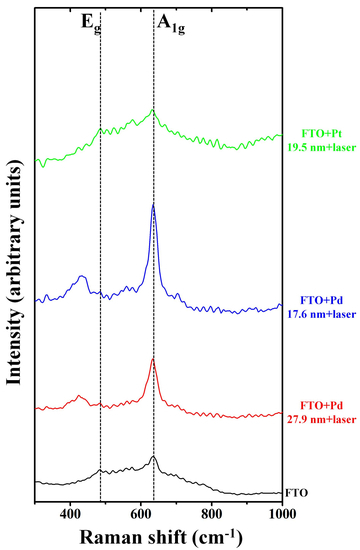
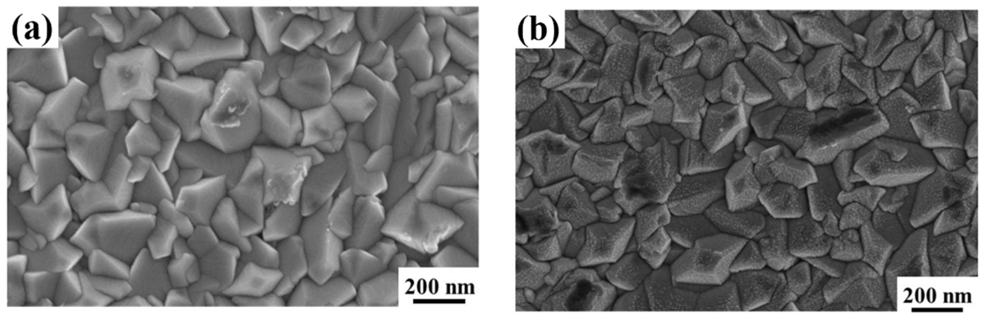
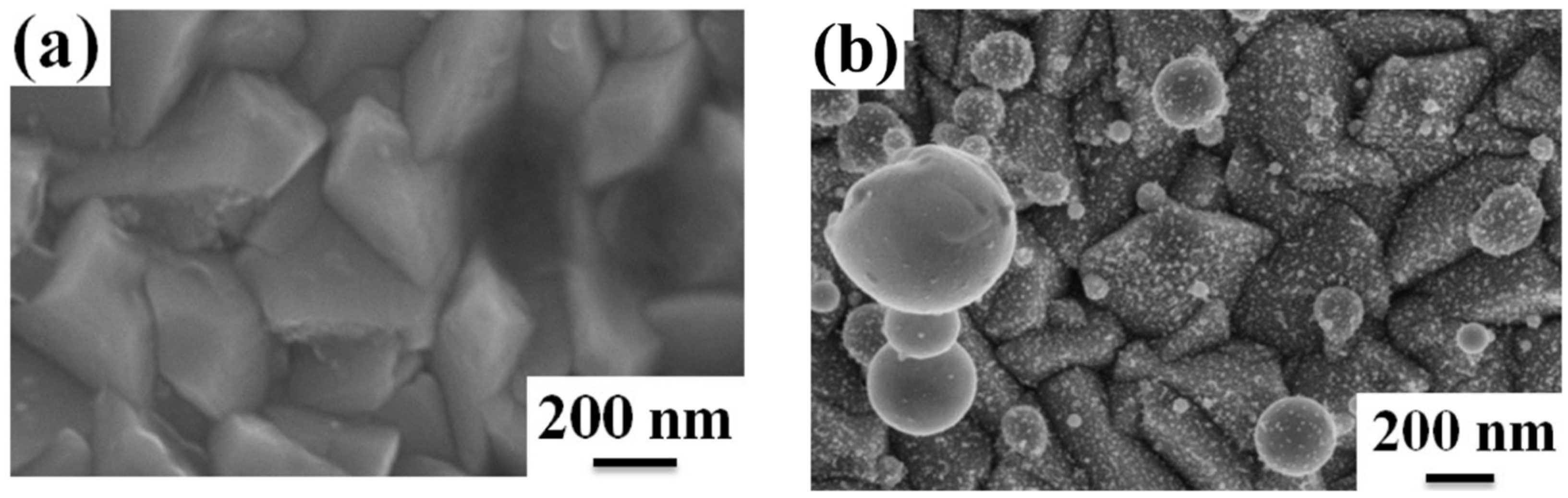
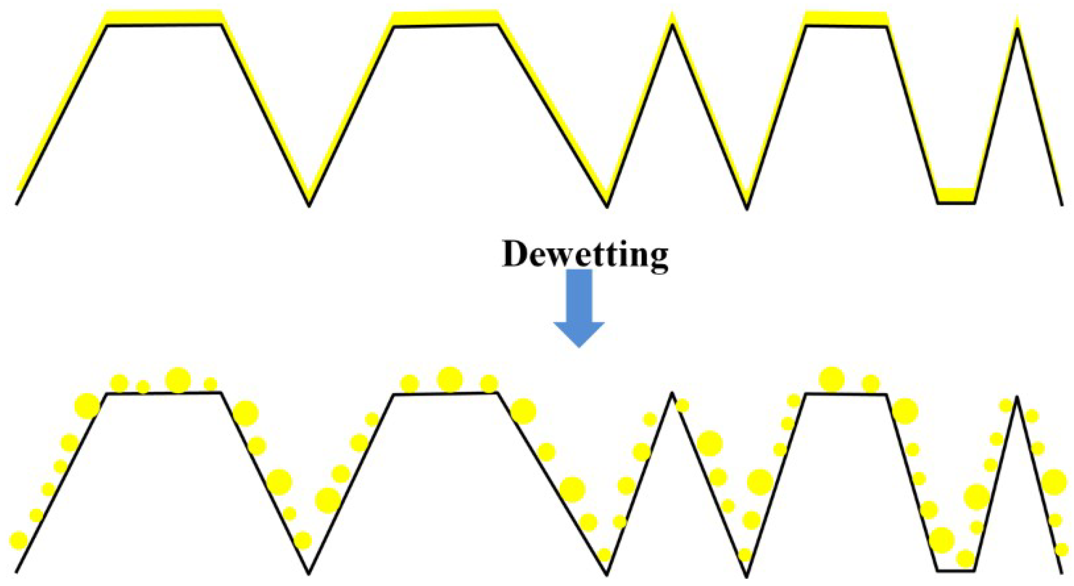
3. Results and Discussion

First, we analyzed, by SEM imaging, the topography of the reference FTO surface. So, Figure 1 reports a typical SEM image of the bare FTO surface. It appears that the FTO layer on the glass substrate has a complex non-flat topography. In fact, by the inspection of this plan-view image, the FTO layer results to be formed by micrometric structures having an approximately truncated-pyramidal shape and which, randomly arranged, cover the entire surface of the glass slide. We point out that this is the standard morphology for deposited FTO layers [38,39] and that it is desired in several applications (solar cells, etc.) due to its ability in efficiently scatter light [17,18,39,41]. Then, in Figure 2 and Figure 3, some exemplificative microscopies of the FTO surface covered by the Pd and Pt films are reported. Figure 2 refers to the Pd covered FTO surface with increasing effective thickness of the covering metal film: dPd = 3.0 nm (a) and dPd = 27.9 nm (b). Figure 3 refers to the Pt covered FTO surface with increasing effective thickness of the covering metal film: dPt =1.9 nm (a) and dPt = 19.5 nm (b). Increasing the amount of sputtered Pd or Pt (i.e., increasing the effective thickness of the deposited metal film), an evolution of the surface morphology can be observed: the pyramidal structuration of the FTO layer is yet recognizable; however, over the pyramids’ surfaces a nano-granular morphology develops (see, in particular, Figure 2b and Figure 3b)
This morphology is the standard one, in the initial stages of growth (i.e., nucleation and growth) for metal films deposited on non-metal substrates and which leading growth process is the Volmer-Weber growth mode [3,17,25,26,31,41,45,46,47].
However, in late stages of growth, increasing the amount of deposited atoms, the nucleated small metal islands grow until to contacting each other giving rise to a coalescing process [45,46,47]. In this stage, a percolative surface morphology of the metal film is obtained in the sense that it is formed by ramified interconnected nano-islands separated by small gaps [45,46,47]. Finally, continuing to deposit more and more material, holes in the growing metal film are filled to form a continuous rough film [45,46,47].
On each metal-covered sample, we carried out the laser irradiation. Then, we used the SEM analysis to study the metal surface morphology evolution versus the metal film thickness, see Figure 4 and Figure 5. In general, the pulsed laser-induced dewetting of the metal film is observed, that is, the 0.50 J/cm2 laser irradiation for 12 ns causes the melting of the Pd or Pt film followed by the film rupture and retreating processes towards the formation of NPs of circular section (Figure 4 and Figure 5). The spherical (or almost-spherical) shape of the NPs can be easily recognized from the SEM images in Figure 4 and Figure 5 where in several cases NPs are observed from a tilted configuration due to the surface structuration of the FTO surface (i.e., the NPs placed on the lateral surfaces of the FTO pyramids). In fact, generally, metal films on transparent conductive oxides are highly non-wetting systems [26] so that, after the dewetting process, spherical or almost-spherical NPs are obtained (i.e., maximization of the contact angle).
In particular, Figure 4 presents typical SEM microscopies showing the Pd NPs originated from the pulsed laser irradiation of the FTO-supported Pd film having thickness (a) 3.0 nm or (b) 27.9 nm; in addition, Figure 5 presents SEM microsopies showing the Pt NPs originated from the irradiation of the FTO-supported Pt film with thickness (a) 1.9 nm (no NPs formation) and (b) 19.5 nm.
It is, nowadays, well-established [17,22,23,24,25,26,27,41,42,43] that during the nanosecond pulsed laser irradiation of deposited nanoscale-thick metal films, the NPs are formed from the continuous films by a molten-phase dewetting process. In fact, in standard metals (such as Pd and Pt) the thermal equilibrium between hot electrons and phonons is established, typically, within a characteristic time teq ≈ 50 ps [17,22,23,24,25,26,27,41,42,43,48]. Using nanosecond pulsed laser to generate heat in the film, as in the present experiments for which the pulse duration is τ = 12 ns so that τ >> teq, then the metal film melting dynamics is the main process [17,22,23,24,25,26,27,41,42,43,48]. Therefore, in the present experiments, the Pd and Pt dewetting process occurs with the films being in the molten state (i.e., spinodal dewetting [17,22,23,24,25,26,27,41,42,43,48]) followed by the film’s solidification. Shortly, it is widely accepted that this dewetting process starts by the film perforation which leads to holes formation in the film. These perforations are likely to occur where the film is thinner since the fluence required for melting is lower for thinner films [24]. Deposited metal films, in fact, are, typically, not perfectly uniform in thickness presenting, instead, a natural roughness (local variation in thickness). The metal at the hole edges forms the so-called rims which retract drawing away from the center of the hole. The retreating molten films in neighboring holes coalesce into metal filaments (some solidified Pd filaments are recognizable, for example, in Figure 4a). These filaments are thermodynamically unstable so that, then, then split into droplets by the Rayleigh instability [24,25,26,27] and minimizing the total surface energy of the system. In the final stage, after solidification, an array of metal NPs uniformly covering the laser-irradiated surface is obtained.
We proceeded, then, to the quantitative analysis of the Pd and Pt NPs characteristics using the SEM images. In particular, for each sample, distributions of the NPs diameter D were constructed as described in the experimental section. As an example of the procedure, Figure 6a reports a part of the SEM image of Figure 4a concerning the NPs obtained by the laser irradiation of the 3 nm-thick Pd film and in Figure 6b how it was treated in luminosity and contrast to identify the NPs (circular white regions). Using the scale marker, for each circular region the diameter can be identified so to construct the NPs diameters distribution. In addition, by direct counting of the circular white regions, the NPs surface density can be derived.
Figure 7 reports, then, some examples of obtained diameter distributions: (a,b) are the diameters for the NPs obtained by the laser irradiation of the 3 nm-thick ((a)) and 27.9 nm-thick ((b)) Pd films deposited on the FTO surface; (c,d) are the diameter distributions for the NPs obtained by the laser irradiation of the 7.5 nm-thick ((c)) and 19.5 nm-thick ((d)) Pt films deposited on the FTO surface. As easily recognizable, (a,c) shows a monomodal size distribution while (b,d) bimodal sizes distributions.
Each diameter’s distribution was, hence, statistically analyzed to extract the mean diameter <D> (and the corresponding standard deviation ΔD) of the NPs. In addition, we evaluated, also, the mean NPs surface density <N> and the corresponding errors. The results are summarized in the plots in Figure 8. In particular, performing these analyses, in some samples we observed a monomodal size distribution (one gaussian distribution) indicative of an unique NPs population to which was associated an uniqhe mean diameter <D> and mean NPs surface density <N>. In other samples, we observed a bimodal size ditribution (two gaussian distributions) indicative of two NPs sub-populations to which were associated mean diameters <D1> and <D2> and mean NPs surface densities <N1> and <N2>.
Specific values for <D1>, <D2>, <N1> and <N2> are, further, summarized in Table 1 for the various samples.
To discuss these data, first of all we recall some basis of the thin metal film melting process induced by pulsed laser irradiations. In the first approximation, a simple model [24,26] considers the metal film of thickness d as irradiated by one laser pulse of duration τ with a top-hat temporal profile and establishes (as reliable hypothesis) the total heat (per unit area) generated in the film as S = Iτ(1−r)[1-exp(-αd)] being I the laser pulse intensity (W/cm2), r the film reflectivity at the laser wavelength, α−1 the film optical absorption length at the laser wavelength (α is called the absorption coefficient). Note, however, that for a thin film, r and α depend on d. On the basis of this model, the consequent temperature rise in the thin film is ΔT = S/Cd where C is the film heat capacity per unit volume. So, the melting (and molten-phase dewetting) characteristics of a thin metal film depend on optical and thermal characteristics of the film (d, r, α, C, melting temperature). In principle, differences in these parameters for Pd and Pt justify the observed differences in <D> and <N> when fixed the film thickness, the laser fluence and pulse duration. This is the case for the 7.5 nm-thick Pd and Pt films for which, on the same substrate, two Pd NPs populations and an unique Pt NPs population are, respectively, obtained. On the other hand, it is easy to understand why the laser irradiation of the 1.9 nm-thick Pt film does not produce a dewetting process (i.e., formation of the NPs). In this case, clearly, d<<α−1 (for metal films, generally, α−1~10 nm) and/or r is so low that the Pt film does not absorb energy from the laser pulse: the film temperature does not change and the film is unaffected by the laser irradiation.
Shortly, we also discuss the laser irradiation effect on the underlaying FTO substrate. In fact, the melting temperatures for Pt and Pd are, about, 2040 and 1828 K, respectively, while the melting temperature for the SnO2 is around 1900 K. So, in the laser irradiation processes we could expect, also, a partial melting of the FTO substrate due to the high temperatures achieved for melting, at least, the Pt films. To discuss this point, for example, we recall the results obtained by Font et al. [49] regarding the heat transfer mechanisms involved in thin metal films melting on a SiO2 layer and exposed to laser irradiation. In this work, the authors present a model describing the heat transfer and phase change of the metal/substrate system during nanosecond laser irradiation with parameters similar to those presented in our work. In particula, Font et al. [49] considered a Cu film/10 nm-thick SiO2 layer/Si substrate system irradiated by a pulsed laser characterized by a Gaussian beam, and they studied the effect of the laser parameters, including energy density and pulse duration, on possible melting of the SiO2 layer. Interestingly, they found that maximum thickness of the melted SiO2 region can be of the same order of magnitude as the thickness of the metal film. The calculations carried out by the authors are based on some assumptions. In particular, for example, they supposed that the substrate is completely transparent to the laser radiation, so that the metal film absorbs the energy of the laser and transfers it to the substrate by conduction. This condition is fulfilled, also, by the FTO/glass substrate used for the experiments presented by us. To describe the heating and possible melting of the substrate, they considered, obviously, heat conduction in each layer of the system. In the basing equations, so, the thermal conductivity of the SiO2 layer (in solid and liquid phases) is involved. This value, however, is very different from that characterizing the FTO layer. In fact, for example, in the solid phase, for SiO2 typical value for the thermal conductivity is 1.4 W/m·K [49]. Instead, SnO2 is characterized by a much higher thermal conductivity, of the order of 40 W/m·K [50]. Clearly, the temperature increase in the film depends on how it dissipates the laser-generated heat [24]: concerning a metal film deposited on a low thermal conductive substrate, the laser-generated heat will remain, mostly, confined in the metal film resulting in a higher increase of temperature of the system. This means that for the metal films deposited on the FTO substrate the rapid dissipation of the laser-generated heat through the FTO substrate results in a lower increase of the system temperatrure compared to the case for which the same metal films are deposited on a lower thermal conductivity substrate (as SiO2). In fact, comparing the SEM images in Figure 4 and Figure 5 (Pd and Pt films on FTO after the laser irradiations) to the SEM image in Figure 1 (bare and untreated FTO), it seems clear that the surface morphology of the FTO substrate is unchanged after the laser irradiations. This is an indication of the fact that even if the laser-generated heat determines the temperature increase of the metal films above the film material melting temperature, the relatively high thermal conductivity of the FTO probably results in a temperature increase of the FTO layer below its melting temperature. This is the situation for the 0.50 J/cm2 laser pulse. This situation is strongly changed, for example, using a 0.75 J/cm2 laser pulse for which the SEM images (not shown) clearly showed a dramatic change of the FTO surface morphology: in this case, the FTO pyramids are no more recognizable being the FTO surface more similar to a flat surface. This is, probably, consequence of the higher temperature reached by the FTO layer, higher than the FTO melting temperature. In this case, so, also the FTO layer melts during the laser irradiations and, also, an FTO morphology change is involved in the overall process. This is a further reason for which we limit the data presented here to the 0.50 J/cm2 laser pulse, so involving only the Pd and Pt molten-phase dewetting process.
Regarding the standard dewetting process of metal films on flat surfaces [22,23,24,25,26,27,28,29,30,31], a unique NPs population is expected with a mean size, which increases by increasing the starting thickness of the deposited film. The observation of the formation of two different NP populations in some samples is, thus, indicative of the effect of the substrate non-flat surface topography on the film dewetting process, influencing, then, the size of the NPs. To describe this effect we, briefly, discuss some of the results due to Gierman and Thompson [33]. They intentionally patterned, by using electron beam litography, a SiO2 surface in spatially ordered arrays of inverted pyramid shaped pits. However, different patterns were designed by changing the spatial period of the pits (175 or 377 nm) and the pit-to-mesa width ratio (1.5, 1.9, 5.3). Onto the so-patterned SiO2 surface, Au films of different thickness (16, 21, 32 nm) were evaporated. The Au films solid-state dewetting process was activated by 800 °C annealing process. The microscopic analysis revealed for the resulting Au NPs originated in the dewetting process, a spatial arrangement on the substrate surface and size distribution dependent on the geometric characteristics of the surface pattern (spatial period of the pits and pit-to-mesa width ratio) in combination with the Au film thickness. On the basis of the combination of these parameters: in some cases the preferential formation of a single NP per pits with no NPs on the mesa was observed; in other cases, the formation of one NP per pit with some other NPs on the mesa was achieved; in further cases, the generation of multiple NPs per pit with some other NPs on the mesa resulted; finally, some other combinations lead to the formation of large NPs on the mesa (often covering the pits) with no NPs in the pits. These results clearly demonstrated the crucial effect of the surface topography on the deposited metal film dewetting also giving the possibility to study, quantitatively, this effect taking into in account the excess of local chemical potential as modulated by the finite local curvatures on the substrate surface [33]. In fact, considering the dewetting process of a thin metal film on a flat surface, it is clear that the driving force for the process is, solely, the minimization of the total surface and interface energy of the system. For a flat surface, the local radius of curvature is, in each surface point, R → ∞. The corresponding local curvature is κ = 1/R to which is related, by the Gibbs–Thomson relation, the local excess of chemical potential Δμ = κγΩ → 0 (being γ the film surface energy and Ω film atomic volume. Consequently, the dewetting process of a thin film on a flat surface is not affected by the surface topography. The situation changes if the surface is not flat, that is, if it presents finite local curvatures (as in the case of the patterned surfaces used by Giermann and Thompson). In this case, due to the finite values of R, the non-zero values of Δμ = κγΩ introduce an additional driving force for the film dewetting process determining, in particular, a preferential material diffusion from the positions with κ > 0 (peaks or ridges) to the positions with κ < 0 (valleys), see the representative scheme in Figure 9. It is clear, then, the modulation of Δμ through the surface geometry impacts on the dewetting process and on the resulting characteristics (spatial arrangement and size) of the NPs originanting from this process. Refererring to the specific case reported by Giermann and Thompson [33], which is particularly useful for the interpretation of our data, the edge of a pit is characterized by a Δμ ∝ 1/RA > 0 while the apex of an inverted pyramid is characterized by Δμ ∝ −1/|RB| < 0, see Figure 9. It follows that, to minimize the total surface and interface energy of the system and to establish a global condition for which Δμ = 0, the film material will diffuse away from the pit edge toward the pit apex and here, preferentially, will form the NPs. However, since the local curvature at the pit edge and the apex decreases with increasing film thickness, the driving force for flow from the edge to the apex also decreases with increasing film thickness. So, overall, the effect becomes dependent on the film thickness.
In our case, we observed that increasing the thickness of the Pd film from 3.5 to 27.9 nm and of the Pt film from 7.5 to 19.5 nm, the NPs population evolves from monomodal to bimodal. This indicates the existence of a critical film thickness dc identifying a variation in the dewetting characteristics of the film, as pictured by the combination of Figure 10 and Figure 11. For d < dc (generally named “low-thickness” condition) the substrate topography does not affect the film dewetting process (Figure 10). In this condition, the film does not interact with the topographic features of the substrate and, then, the substrate behaves as a flat substrate with respect to the film dewetting. Hence, the film dewets as on a planar substrate originating NPs uniformly arranged over the surface of the substrate. In addition, the size of the dewetted NPs, being the starting thickness of the deposited film very low with respect to local surface curvatures (defined by the characteristic sizes of the FTO pyramids, i.e., height, width, spacing), is not influenced by the substrate topography. For d > dc (generally named “high-thickness” condition) the geometrical features of the substrate affect the film dewetting process and, hence, the resulting mean size of the formed NPs (Figure 11). In this case the thickness of the deposited film is, at least, comparable to the local surface curvatures. Then, the film dewetting is driven, in addition to the surface energy minimization, by the surface topography through the local excess of chemical potential. This results in the preferential formation of the NPs in-between or over the pyramids. It is clear, hence, that the characteristic sizes of the FTO pyramids affects the final NPs mean size. The overall effect is determined by an interplay between these characteristic sizes (establishing the local surface curvatures) and the thickness d of the film. Therefore, observing Figure 8, in that samples where an unique population of NPs is obtained, the situation d < dc is realized (dewetting as on a flat surface), whereas in that samples where a two NPs sub-populations are obtained, the situation d > dc is realized (substrate topography-driven dewetting). Then, we can conclude, also, that 3 nm < dc < 7.5 nm for the Pd film and that 7.5 nm < dc < 12.2 nm for the Pt film. However, for sake of completeness, we also mention that, according to previous experimental and theoretical studies on dewetting of films on patterned surfaces [51,52,53,54], a critical thickness dc for the film separating different effects of the substrate topography on the dewetting process is related to additional parameters than the local excess of chemical potential Δμ. In particular, it is known that a fixed substrate pattern can influence the dewetting pathways of supported film depending on the film thickness by acting on the length-scale of the processes (holes nucleation, film retreating, Rayleigh instability, etc.) involved in the dewetting phenomenon. Dewetting on a flat substrate progresses with the formation and growth of randomly placed holes with a certain mean length-scale. Eventually, coalescence of holes produces an isotropic collection of droplets. The average diameters of the dewetted structures depend on the initial film thickness. On the other hand, specific spatial periodicity of patterns on the substrate can act on a deposited film by imposing conditions on the length-scale of the processes involved in the dewetting phenomenon (in addition to the effect imposed by local excess of chemical potential on the material film diffusive processes). An a-priori theoretical determination of the critical thickness dc should take into in account, also, such effects but this is out of the scope of the present experiments.
To conclude the analyses of the characteristics of the Pd and Pt NPs produced on the FTO substrate, we performed, also, Raman analysis. Figure 12 displays, first of all, the Raman spectrum of the bare FTO/glass substrate, in black. There are two fundamental Raman scattering peaks which are those characteristic of rutile SnO2 single crystal [55]. For pure SnO2, the characteristic and intense band at 625 cm−1 is due to the A1g vibration mode of SnO2. The weak band around 478 cm−1 is due to the Eg vibration modes of SnO2 [55]. Figure 12 reports, also, as examples of the general behaviour, Raman spectra of the FTO/glass substrate covered by Pd or Pt NPs originating from the laser heating of the deposited films: in red the spectrum of the substrate covered by Pd NPs obtained by the laser irradiations of the 27.9 nm-thick Pd film; in blue the spectrum of the substrate covered by Pd NPs obtained by the laser irradiations of the 17.6 nm-thick Pd film, in green the spectrum of the substrate covered by Pt NPs obtained by the laser irradiations of the 19.5 nm-thick Pt film. The general effect is that, compared with bare FTO, the intensity of Pd NPs/FTO samples become stronger.
On the contrary, the presence of the Pt NPs on the FTO surface, does not influence the FTO peak intensity, indicating no Pt NPs-FTO interaction. In particular, the Pd NPs SERS (Surface Enhancement Raman Scattering) enhancement may be due to Pd NPs surface plasmon resonance [5,56,57]. However, surface plasmon resonance effects also for Pt NPs are expected [5]. The reasons for which these effects lead to intense SERS in the Pd NPs/FTO samples while no SERS effects in the Pt NPs/FTO samples is actually under investigation as a perspective work, requiring a crossing of experimental and simulation-based results. Here, we limit to consider that the SERS enhancement should arise from the effective resonance coupling between the localized surface plasmon of the NPs and the characteristic parameters of the energy band structure of the FTO. A match should be realized in the case of the Pd NPs and the FTO, contrary to the case of the Pt NPs and FTO. Besides, several other factors, such as the Ohmic loss, non-radiative Forster energy transfer, lower surface plasmon radiative efficiency, may be responsible for the absence of SERS enhancement in the Pt NPs-FTO systems and these effects have to be considered in a future complete description. However, we mention, for example, that the optical loss of NPs material can be used as a measure to predict the effect in SERS, whereas the optical loss is intended as the imaginary part (ε2) of the dielectric constant ε(ω) = ε1(ω) + iε2(ω) [58]. In fact, the imaginary part of the dielectric constant causes Ohmic damping of the electrons oscillations in the metal. Our SERS data seem in agreement with the consideration that several experimental and theoretical works found higher values of ε2 for bulk, thin films, NPs materials of Pt than of Pd in the UV range [59,60,61].
We observe, finally, in Figure 12, a shift (toward lower wavenumbers) of the Eg peaks in the Pd NPs/FTO samples with respect to the bare FTO substrate, while this shift is absent in the Pt NPs/FTO samples. It is absent, also, before the laser treatment so that it cannot related to substrate modifications due to the sputtering deposition processes. From a general point of view, in Raman spectra, shifting of peaks towards lower or higher wavenumber is related to several factors [62] such as change in the chemical bond length within the sample (the shorter bond length causes to shift higher wavenumber or vice versa), changes in temperature and stress within the sample, and so on. More specifically, a shift in Raman peaks could be due to the addition of oxygen in the sample. In this regard, the fact that this shift is present only in the case of the Pd NPs could suggest its relation to the Pd NPs surface oxidation [63]. It is widely recognized that Pd NPs are subjected to the interaction with environmental oxygen to form a PdO surface shell [64], while Pt NPs are more stable against this reaction [65]. We can support the conclusion that the Raman peak shift for the sample with Pd NPs could be related to surface oxidation of the NPs, by considering that previous works reported wavelength shift of plasmonic bands for Pd NPs [66] and Ag NPs [67,68] after exposure to air or oxygen with consequent formation of surface oxide (PdO or Ag2O) for the NPs. To conclude, we recall that the Pd and Pt NPs produced have a quasi spherical shape and we comment on this fact in view of the Raman measurements results: Raman scattering, which is based on inelastic light scattering upon vibrational excitation of molecules and materials is an extremely inefficient process with about one photon out of 107 being inelastically scattered [69]. This drawback can be overcome when the molecules are located near a rough metal surface or metal NPs, which results in a boost of Raman scattering, in the process known as SERS. Upon resonant excitation of strong localized surface plasmon resonances, a greatly enhanced local electromagnetic field (near-field) is generated at the NP surface. This near-field in turn couples to the incident field and re-reemits radiation with the same wavelength (resonant scattering). As the scattering cross section scales with the square of the polarizability (the degree on how easily the electron cloud can be displaced) also the near-field strongly increases for anisotropic NPs due to higher polarizability, as compared to spheres. So, elongated NPs or those with edges and corners, such as nanorods, nanocubes, and nanotriangles, thus generate strong near-fields concentrated at vertices. The presence of the plasmonic near field at the NP surface upon plasmonic excitation increases the polarizability of an adsorbed molecule (compared to a free molecule) due to mutual excitation between induced dipole in the molecule and induced dipole in the NP and leading to enhanced Raman scattering. On the basis of these considerations, a further perspective on the present work lies in the establishment of laser process parameters to controllably produce complex-morphology Pd and Pt NPs to reach higher SERS enhancements. This could be reached, for example, by using femtosecond pulsed laser irradiations [20,21].

4. Conclusions

Pd and Pt NPs onto non-flat FTO substrate were fabricated by exploiting the molten-phase dewetting process of deposited films. The Pd and Pt films were sputter-deposited on the FTO surface, this surface being constituted this surface by FTO microscopic pyramids randomly distributed over a glass slide. The dewetting process of the liquid metal films was initiated by nanosecond laser irradiations at 0.5 J/cm2, resulting, after solidification, in the formation of Pd or Pt NPs onto the laser-irradiated FTO surface. However, analyzing the mean diameter <D> of the formed NPs versus the thickness d of the deposited films, an effect of the substrate topography was found. This effect was discussed by the description of the substrate topography influence on the excess of chemical potential driving the dewetting process. We observe that increasing the thickness of the Pd film from 3.5 to 27.9 nm and of the Pt film from 7.5 to 19.5 nm, the NPs population evolves from monomodal to bimodal. This indicates the existence of a critical film thickness dc identifying a change in the dewetting characteristics of the film: for d < dc the substrate topography does not influence the film dewetting process, while for d > dc the topography of the substrate is crucial in determining the dewetting process and, so, the final mean size of the produced NPs. In that samples where an unique population of NPs is obtained, the situation d < dc is realized (dewetting as on a flat surface), whereas in that samples where a two NPs sub-populations are obtained, the situation d > dc is realized (substrate topography-driven dewetting). By analyzing the experimental results, we concluded that 3 nm < dc < 7.5 nm for the Pd film and that 7.5 nm < dc < 12.2 nm for the Pt film. Finally, the analysis of the Raman spectra for the bare FTO/glass sample and for the Pd NPs/FTO/glass samples and Pt NPs/FTO/glass samples indicated a SERS effect in the Pd NPs/FTO/glass samples due to the effective coupling between the localized surface plasmon of the Pd NPs and the FTO susbstrate while this effect is absent in the Pt NPs/FTO/glass samples.

Author Contributions

Conceptualization, F.R. and M.G.G.; Methodology, F.R., M.G.G., M.C., V.T.; Formal Analysis, F.R., M.G.G., M.C., V.T.; Investigation, F.R., M.G.G., M.C., V.T., G.P. and G.C.; Data Curation, F.R., M.C., V.T., G.P. and G.C.; Writing—Original Draft Preparation, F.R.; Writing—Review and Editing, F.R., M.G.G., M.C., V.T., G.P. and G.C.; Supervision, F.R., M.G.G.; Funding Acquisition, M.G.G.

Funding

This research received no external funding.

Conflicts of Interest

The authors declare no conflict of interest.

References

  1. Feldheim, D.L.; Foss, C.A. Metal Nanoparticles: Synthesis, Characterization, and Applications; Marcel Dekker Inc.: New York, NY, USA, 2002. [Google Scholar]
  2. Johnston, R.L.; Wilcoxon, J.P. Metal Nanoparticles and Nanoalloys; Elsevier: Amsterdam, The Netherlands, 2012. [Google Scholar]
  3. Ruffino, F.; Crupi, I.; Irrera, A.; Grimaldi, M.G. Pd/Au/SiC nanostructured diodes for nanoelectronics: Room temperature electrical properties. IEEE Trans. Nanotechnol. 2010, 9, 414–421. [Google Scholar] [CrossRef]
  4. Baca, M.; Cendrowski, K.; Kukulka, W.; Bazarko, G.; Moszyński, D.; Michalkiewicz, B.; Kalenczuk, R.J.; Zielinska, B. A Comparison of Hydrogen Storage in Pt, Pd and Pt/Pd Alloys Loaded Disordered Mesoporous Hollow Carbon Spheres. Nanomaterials 2018, 8, 639. [Google Scholar] [CrossRef] [PubMed]
  5. Langhammer, C.; Yuan, Z.; Zorić, I.; Kasemo, B. Plasmonic Properties of Supported Pt and Pd Nanostructures. Nano Lett. 2006, 6, 833–838. [Google Scholar] [CrossRef] [PubMed]
  6. Tran, M.; Whale, A.; Padalkar, S. Exploring the Efficacy of Platinum and Palladium Nanostructures for Organic Molecule Detection via Raman Spectroscopy. Sensors 2018, 18, 147. [Google Scholar] [CrossRef] [PubMed]
  7. Liu, C.; Kuang, Q.; Xie, Z.; Zheng, L. The effect of noble metal (Au, Pd and Pt) nanoparticles on the gas sensing performance of SnO2-based sensors: A case study on the {221} high-index faceted SnO2 octahedra. CrystEngComm 2015, 17, 6308–6313. [Google Scholar] [CrossRef]
  8. Kumar, M.; Bhati, V.S.; Ranwa, S.; Singh, J.; Kumar, M. Pd/ZnO nanorods based sensor for highly selective detection of extremely low concentration hydrogen. Sci. Rep. 2017, 7, 236. [Google Scholar] [CrossRef]
  9. Vendelbo, S.B.; Elkjær, C.F.; Falsig, H.; Puspitasari, I.; Dona, P.; Mele, L.; Morana, B.; Nelissen, B.J.; van Rijn, R.; Creemer, J.F.; et al. Visualization of oscillatory behaviour of Pt nanoparticles catalysing CO oxidation. Nat. Mater. 2014, 13, 884–890. [Google Scholar] [CrossRef]
  10. Kozlov, S.M.; Aleksandrov, H.A.; Neyman, K.M. Energetic Stability of Absorbed H in Pd and Pt Nanoparticles in a More Realistic Environment. J. Phys. Chem. C 2015, 119, 5180–5186. [Google Scholar] [CrossRef] [Green Version]
  11. Crampton, A.S.; Rötzer, M.D.; Schweinberger, F.F.; Yoon, B.; Landman, U.; Heiz, U. Ethylene hydrogenation on supported Ni, Pd and Pt nanoparticles: Catalyst activity, deactivation and the d-band model. J. Catal. 2016, 333, 51–58. [Google Scholar] [CrossRef]
  12. Zhang, J.; Mo, Y.; Vukmirovic, M.B.; Klie, R.; Sasaki, K.; Adzic, R.R. Platinum monolayer electrocatalysts for O2 reduction:  Pt monolayer on Pd(111) and on carbon-supported Pd nanoparticles. J. Phys. Chem. B 2004, 108, 10955–10964. [Google Scholar] [CrossRef]
  13. Park, J.Y. Current Trends of Surface Science and Catalysis; Springer: New York, NY, USA, 2014. [Google Scholar]
  14. Schulte, J. Nanotechnology: Global Strategies, Industry Trends and Applications; John Wiley & Sons Ltd.: Hoboken, NJ, USA, 2005. [Google Scholar]
  15. Rakhshani, A.E.; Makdisi, Y.; Ramazaniyan, H.A. Electronic and optical properties of fluorine-doped tin oxide films. J. Appl. Phys. 1998, 83, 1049–1057. [Google Scholar] [CrossRef]
  16. Elangovan, E.; Ramamurthi, K. A study on low cost-high conducting fluorine and antimony-doped tin oxide thin films. Appl. Surf. Sci. 2005, 249, 183–196. [Google Scholar] [CrossRef]
  17. Ruffino, F.; Gentile, A.; Zimbone, M.; Piccitto, G.; Reitano, R.; Grimaldi, M.G. Size-selected Au nanoparticles on FTO substrate: Controlled synthesis by the Rayleigh-Taylor instability and optical properties. Superlatt. Microstruct. 2016, 100, 418–430. [Google Scholar] [CrossRef]
  18. Ginley, D.S.; Hosono, H.; Paine, D.C. Handbook of Transparent Conductors; Springer: Berlin, Germany, 2010. [Google Scholar]
  19. Kent, C.A.; Concepcion, J.J.; Dares, C.J.; Torelli, D.A.; Rieth, A.J.; Miller, A.S.; Meyer, T.J. Water oxidation and oxygen monitoring by cobalt-modified fluorine-doped TiN oxide electrodes. J. Am. Chem. Soc. 2013, 135, 8432–8435. [Google Scholar] [CrossRef] [PubMed]
  20. Forte, K.; Serbin, J.; Koch, J.; Egbert, A.; Fallnich, C.; Ostendorf, A.; Chichkov, B.N. Towards nanostructuring with femtosecond laser pulse. Appl. Phys. A 2003, 77, 229–235. [Google Scholar]
  21. Moening, J.P.; Thanawala, S.S.; Georgiev, D.G. Formation of high-aspect-ratio protrusions on gold films by localized pulsed laser irradiation. Appl. Phys. A 2009, 95, 635–638. [Google Scholar] [CrossRef]
  22. Favazza, C.; Kalayanaraman, R.; Sureshkumar, R. Dynamics of ultrathin metal films on amorphous substrates under fast thermal processing. J. Appl. Phys. 2007, 102, 104308. [Google Scholar] [CrossRef] [Green Version]
  23. Henley, S.J.; Carrey, J.D.; Silva, S.R.P. Metal nanoparticle production by pulsed laser nanostructuring of thin metal films. Appl. Surf. Sci. 2007, 253, 8080–8085. [Google Scholar] [CrossRef]
  24. Trice, J.; Thomas, D.; Favazza, C.; Sureshkumar, R.; Kalyanaraman, R. Pulsed-laser induced dewetting in nanoscopic metal films: Theory and experiments. Phys. Rev. B 2007, 75, 235439. [Google Scholar] [CrossRef]
  25. Ruffino, F.; Pugliara, A.; Carria, E.; Bongiorno, C.; Spinella, C.; Grimaldi, M.G. Formation of nanoparticles from laser irradiated Au thin films on SiO2/Si: Elucidating the Rayleigh-instability role. Mater. Lett. 2012, 84, 27–30. [Google Scholar] [CrossRef]
  26. Ruffino, F.; Carria, E.; Kimiagar, S.; Crupi, I.; Simone, F.; Grimaldi, M.G. Formation and evolution of nanoscale metal structures on ITO surface by nanosecond laser irradiations of thin Au and Ag films. Sci. Adv. Mater. 2012, 4, 708–718. [Google Scholar] [CrossRef]
  27. Ruffino, F.; Grimaldi, M.G. Controlled dewetting as fabrication and patterning strategy for metal nanostructures. Phys. Status Solidi A 2015, 212, 1662–1684. [Google Scholar] [CrossRef]
  28. González, A.G.; Diez, J.A.; Wu, Y.; Fowlkes, J.D.; Rack, P.D.; Kondic, L. Instability of liquid Cu films on a SiO2 substrate. Langmuir 2013, 29, 9378–9387. [Google Scholar] [CrossRef]
  29. Fowlkes, J.D.; Kondic, L.; Diez, J.; Rack, P.D. Self-assembly versus directed assembly of nanoparticles via pulsed laser induced dewetting of patterned metal films. Nano Lett. 2011, 11, 2478–2485. [Google Scholar] [CrossRef] [PubMed]
  30. Ruffino, F.; Pugliara, A.; Carria, E.; Romano, L.; Bongiorno, C.; Fisicaro, G.; La Magna, A.; Spinella, C.; Grimaldi, M.G. Towards a laser fluence dependent nanostructuring of thin Au films on Si by nanosecond laser irradiation. Appl. Surf. Sci. 2012, 258, 9128–9137. [Google Scholar] [CrossRef]
  31. Thompson, C.V. Solid-State Dewetting of Thin Films. Annu. Rev. Mater. Res. 2012, 42, 399–434. [Google Scholar] [CrossRef]
  32. Kwon, J.-Y.; Yoon, T.-S.; Kim, K.-B.; Min, S.-H. Comparison of the agglomeration behavior of Au and Cu films sputter deposited on silicon dioxide. J. Appl. Phys. 2003, 93, 3270–3278. [Google Scholar] [CrossRef]
  33. Giermann, A.L.; Thompson, C.V. Solid-state dewetting for ordered arrays of crystallographically oriented metal particles. Appl. Phys. Lett. 2005, 86, 121903. [Google Scholar] [CrossRef]
  34. Wang, D.; Ji, R.; Schaaf, P. Formation of precise 2D Au particle arrays via thermally induced dewetting on pre-patterned substrates. Beilstein J. Nanotechnol. 2011, 2, 318–326. [Google Scholar] [CrossRef]
  35. Wang, D.; Schaaf, P. Solid-state dewetting for fabrication of metallic nanoparticles and influences of nanostructured substrates and dealloying. Phys. Status Solidi A 2013, 210, 1544–1551. [Google Scholar] [CrossRef]
  36. Yang, S.; Xu, F.; Ostendorp, S.; Wilde, G.; Zhao, H.; Lei, Y. Template-confined dewetting process to surface nanopatterns: Fabrication, structural tunability, and structure-related properties. Adv. Funct. Mater. 2011, 21, 2446–2455. [Google Scholar] [CrossRef]
  37. Ruffino, F.; Grimaldi, M.G. Self-organized patterned arrays of Au and Ag nanoparticles by thickness-dependent dewetting of template-confined films. J. Mater. Sci. 2014, 49, 5714–5729. [Google Scholar] [CrossRef]
  38. Wang, J.T.; Shi, X.L.; Liu, W.W.; Zhong, X.H.; Wang, J.N.; Pyrah, L.; Sanderson, K.D.; Ramsey, P.M.; Hirata, M.; Tsuri, K. Influence of preferred orientation on the electrical conductivity of fluorine-doped TiN oxide films. Sci. Rep. 2014, 4, 3679. [Google Scholar] [CrossRef] [PubMed]
  39. Wang, J.T.; Shi, X.L.; Zhong, X.H.; Wang, J.N.; Pyrah, L.; Sanderson, K.D.; Ramsey, P.M.; Hirata, M.; Tsuri, K. Morphology control of fluorine-doped tin oxide thin films for enhanced light trapping. Sol. Energy Mater. Sol. Cells 2015, 132, 578–588. [Google Scholar] [CrossRef]
  40. Ruffino, F. Experimental analysis on the molten-phase dewetting characteristics of AuPd Alloy films on topoghraphically-structured substrates. Metals 2017, 7, 327. [Google Scholar] [CrossRef]
  41. Gentile, A.; Cacciato, G.; Ruffino, F.; Reitano, R.; Scapellato, G.; Zimbone, M.; Lombardo, M.; Battaglia, A.; Gerardi, C.; Foti, M.; et al. Nanoscale structuration and optical properties of thin gold films on textured FTO. J. Mater. Sci. 2014, 49, 8498–8507. [Google Scholar] [CrossRef]
  42. Zhou, Z.; Song, Z.; Li, L.; Zhang, J.; Wang, Z. Fabrication of periodic variable-sized Pt nanoparticles via laser interference patterning. Appl. Surf. Sci. 2015, 335, 65–70. [Google Scholar] [CrossRef]
  43. Owusu-Ansah, E.; Horwood, C.A.; El-Sayed, H.A.; Birss, V.I.; Shi, Y.J. A method for the formation of Pt metal nanoparticles using nanosecond pulsed laser dewetting. Appl. Phys. Lett. 2015, 106, 203103. [Google Scholar] [CrossRef]
  44. Available online: http://www.kintec.hk/ (accessed on 10 November 2018).
  45. Venables, J.A.; Spiller, G.D.; Hanbücken, M. Nucleation and growth of thin films. Rep. Prog. Phys. 1984, 47, 399–459. [Google Scholar] [CrossRef]
  46. Ruffino, F.; Grimaldi, M.G. Island-to-percolation transition during the room-temperature growth of sputtered nanoscale Pd films on hexagonal SiC. J. Appl. Phys. 2010, 107, 074301. [Google Scholar] [CrossRef]
  47. Zhang, L.; Cosandey, F.; Persaud, R.; Madey, T.E. Initial growth and morphology of thin Au films on TiO2(110). Surf. Sci. 1999, 439, 73–85. [Google Scholar] [CrossRef]
  48. Li, Y.; Tang, C.; Zhong, J.; Meng, L. Dewetting and detachment of Pt nanofilms on graphitic substrates: A molecular dynamics study. J. Appl. Phys. 2015, 117, 064304. [Google Scholar] [CrossRef]
  49. Font, F.; Afkhami, S.; Kondic, L. Substrate melting during laser heating of nanoscale metal films. Int. J. Heat Mass Transf. 2017, 113, 237–245. [Google Scholar] [CrossRef]
  50. Poulier, C.; Smith, D.S.; Absi, J. Thermal conductivity of pressed powder compacts: Tin oxide and alumina. J. Eur. Ceram. Soc. 2007, 27, 475–478. [Google Scholar] [CrossRef]
  51. Lu, L.-X.; Wang, Y.-M.; Srinivasan, B.M.; Asbahi, M.; Yang, J.K.W.; Zhang, Y.-W. Nanostructure formation by controlled dewetting on patterned substrates: A combined theoretical, modeling and experimental study. Sci. Rep. 2016, 6, 32398. [Google Scholar] [CrossRef] [PubMed]
  52. Mukherjee, R.; Bandyopadhyay, D.; Sharma, A. Control of morphology in pattern directed dewetting of thin polymer films. Soft Matter 2008, 4, 2086–2097. [Google Scholar] [CrossRef]
  53. Kargupta, K.; Sharma, A. Dewetting of thin films on periodic physically and chemically patterned surfaces. Langmuir 2002, 18, 1893–1903. [Google Scholar] [CrossRef]
  54. Kargupta, K.; Sharma, A. Templating of thin films induced by dewetting on patterned surfaces. Phys. Rev. Lett. 2001, 86, 4536–4539. [Google Scholar] [CrossRef] [PubMed]
  55. Liu, H.; Wang, A.; Sun, Q.; Wang, T.; Zeng, H. Cu Nanoparticles/fluorine-doped TiN oxide (FTO) nanocomposites for photocatalytic H2 evolution under visible light irradiation. Catalysts 2017, 7, 385. [Google Scholar] [CrossRef]
  56. Lu, X.; Rycenga, M.; Skrabalak, S.E.; Wiley, B.; Xia, Y. Chemical synthesis of novel plasmonic nanoparticles. Annu. Rev. Phys. Chem. 2009, 60, 167–192. [Google Scholar] [CrossRef] [PubMed]
  57. Sugawa, K.; Tahara, H.; Yamashita, A.; Otsuki, J.; Sagara, T.; Harumoto, T.; Yanagida, S. Refractive index susceptibility of the plasmonic Palladium nanoparticle: Potential as the third plasmonic sensing material. ACS Nano 2015, 9, 1895–1904. [Google Scholar] [CrossRef] [PubMed]
  58. Maier, S.A. Plasmonics-Fundamental and Applications; Springer: New York, NY, USA, 2007. [Google Scholar]
  59. Windt, D.L.; Cash, W.C.; Scott, M.; Arendt, P.; Newnam, B.; Fisher, R.F.; Swartlander, A.B. Optical constants for thin films of Ti, Zr, Nb, Mo, Ru, Rh, Pd, Ag, Hf, Ta, W, Re, Ir, Os, Pt, and Au from 24 Å to 1216 Å. Appl. Opt. 1988, 27, 246–278. [Google Scholar] [CrossRef] [PubMed]
  60. Rakić, A.D.; Djurišić, A.B.; Elazar, J.M.; Majewski, M.L. Optical properties of metallic films for vertical-cavity optoelectronic devices. Appl. Opt. 1998, 37, 5271–5283. [Google Scholar] [CrossRef] [PubMed]
  61. Werner, W.S.M.; Glantschnig, K.; Ambrosch-Draxl, C. Optical constants and inelastic electron-scattering data for 17elemental metals. J. Phys. Chem. Ref. Data 2009, 38, 1013–1092. [Google Scholar] [CrossRef]
  62. Turrell, G.; Corset, J. Raman Microscopy: Developments and Applications; Elsevier Academic Press: Amsterdam, The Netherlands, 1996. [Google Scholar]
  63. Han, Y.; Lupitskyy, R.; Chou, T.-M.; Stafford, C.M.; Du, H.; Sukhishvili, S. Effect of Oxidation on Surface-Enhanced Raman Scattering Activity of Silver Nanoparticles: A Quantitative Correlation. Anal. Chem. 2011, 83, 5873–5880. [Google Scholar] [CrossRef]
  64. Westerström, R.; Messing, M.E.; Blomberg, S.; Hellman, A.; Grönbeck, H.; Gustafson, J.; Martin, N.M.; Balmes, O.; van Rijn, R.; Andersen, J.N.; et al. Oxidation and reduction of Pd(100) and aerosol-deposited Pd nanoparticles. Phys. Rev. B 2011, 83, 115440. [Google Scholar] [CrossRef] [Green Version]
  65. Yoshida, H.; Omote, H.; Takeda, S. Oxidation and reduction processes of platinum nanoparticles observed at the atomic scale by environmental transmission electron microscopy. Nanoscale 2014, 6, 13113–13118. [Google Scholar] [PubMed]
  66. Kracher, M.; Worsch, C.; Rüssel, C. Optical properties of palladium nanoparticles under exposure of hydrogen and inert gas prepared by dewetting synthesis of thin-sputtered layers. J. Nanopart. Res. 2013, 15, 1594. [Google Scholar] [CrossRef]
  67. Yin, Y.; Li, Z.-Y.; Zhong, Z.; Gates, B.; Xia, Y.; Venkateswaran, S. Synthesis and characterization of stable aqueous dispersions of silver nanoparticles through the Tollens process. J. Mater. Chem. 2002, 12, 522–527. [Google Scholar] [CrossRef]
  68. Lok, C.-N.; Ho, C.-M.; Chen, R.; He, Q.-Y.; Yu, W.-Y.; Sun, H.; Tam, P.K.-H.; Chiu, J.-F.; Che, C.-M. Silver nanoparticles: Partial oxidation and antibacterial activities. J. Biol. Inorg. Chem. 2007, 12, 527–534. [Google Scholar] [CrossRef]
  69. Reguera, J.; Langer, J.; Jiménez de Aberasturi, D.; Liz-Marzán, L.M. Anisotropic metal nanoparticles for surface enhanced Raman scattering. Chem. Soc. Rev. 2017, 46, 3866–3885. [Google Scholar] [CrossRef] [PubMed]
Figure 1. FTO bare surface as imaged by SEM. The surface structuration in pyramidal-like structures is recognizable.
Coatings 09 00068 g001
Figure 2. SEM images of the FTO surface covered by Pd film with effective thickness of: (a) 3 nm; (b) 27.9 nm. The presence of the films can be recognized in more rough pyramids surfaces with respect to bare surfaces.
Coatings 09 00068 g002
Figure 3. SEM images of the FTO surface covered by Pt film with effective thickness of: (a) 1.9 nm, (b) 19.5 nm. The presence of the films can be recognized in more rough pyramids surfaces with respect to bare surfaces.
Coatings 09 00068 g003
Figure 4. SEM images of the FTO surface covered by Pd film after the 0.50 J/cm2 laser pulse ((a) 3 nm-thick, (b) 27.9 nm-thick. The formation of almost-spherical particles on the FTO surface is recognizable both in (a,b).
Coatings 09 00068 g004
Figure 5. SEM images of the FTO surface covered by Pt film after the 0.50 J/cm2 laser pulse ((a) 1.9 nm-thick; (b) 19.5 nm-thick). In (a) the Pt film is unchanged, while in (b) the formation of almost-spherical particles on the FTO surface is recognizable.
Coatings 09 00068 g005
Figure 6. (a) SEM image showing the NPs produced on the FTO surface after the laser irradiation of the 3 nm-thick deposited Pd film (it is a part of the SEM image in Figure 4a). (b) SEM image in (a) suitably treated in luminosity and contrast to identify the NPs (circular white regions) so to extract NPs size and number per unit area.
Coatings 09 00068 g006
Figure 7. Examples of NPs diameter distributions: The diameters distributions for the NPs obtained by the laser irradiation of the (a) 3 nm-thick and (b) 27.9 nm-thick Pd films deposited on the FTO surface; The diameters distributions for the NPs obtained by the laser irradiation of the (c) 7.5 nm-thick and (d) 19.5 nm-thick Pt films deposited on the FTO surface. As easily recognizable, (a,c) shows a monomodal size distribution while (b,d) bimodal sizes distributions.
Coatings 09 00068 g007aCoatings 09 00068 g007b
Figure 8. Mean diameter <D> ((a)) and mean surface density <N> ((b)) of the Pd NPs obtained by the 0.50 J/cm2 laser irradiation of the 3 nm, 7.5 nm, 17.6 nm, 27.9 nm thick deposited Pd films. Mean diameter <D> ((c)) and mean surface density <N> ((d)) of the Pt NPs obtained by the 0.50 J/cm2 laser irradiation of the 1.9, 7.5, 12.2, 19.5 nm-thick deposited Pt films. The indication of two values for <D> or <N> for the same sample means the presence of two different NPs sub-populations in that sample.
Coatings 09 00068 g008
Figure 9. Representation of a thin film conformally covering a patterned surface. The curvature at the pit edge, RA, and at the inverted apex, RB are shown. Reprinted with permission from [33]. Copyright 2005 AIP Publishing.
Coatings 09 00068 g009
Figure 10. Picture of the result of the “low-thickness”-film dewetting process on the FTO topographically structured surface. Small NPs are uniformly distributed over the entire FTO surface (as on a flat surface).
Coatings 09 00068 g010
Figure 11. Picture of the result of the “high-thickness”-film dewetting process on the FTO topographically structured surface. Large NPs are preferentially formed in-between or over the FTO pyramids.
Coatings 09 00068 g011
Figure 12. Raman spectra corresponding to the bare FTO substrate (black), FTO covered by Pd NPs obtained by the laser irradiation of the 27.9 nm-thick Pd film (red) and of the 17.6 nm-thick Pd film (blue), FTO covered by Pt NPs obtained by the laser irradiation of the 19.5 nm-thick Pt film. SERS effect can be particularly recognized in the blue spectrum.
Coatings 09 00068 g012
Table 1. Summary of the values of <D1>, <D2>, <N1>, <N2> for the NPs in the samples.
Thickness of the Film-Material<D1> (nm)<N1> (×109 cm−2)<D2> (nm)<N2> (×109 cm−2)
3 nm-Pd~50~4.500
7.5 nm-Pd~75~2~100~0.5
17.6 nm-Pd~70~1.5~150~1.5
27.9 nm-Pd~100~2~220~2
1.9 nm-Pt0000
7.5 nm-Pt~70~3.200
12.2 nm-Pt~75~0.6~220~0.6
19.5 nm-Pt~70~1.6~180~2.7

