Article

A Deep Insight into the Electronic Properties of CIGS Modules with Monolithic Interconnects Based on 2D Simulations with TCAD

by
Ricardo Vidal Lorbada
1,2,*,
Thomas Walter
2,
David Fuertes Marrón
1,
Tetiana Lavrenko
2 and
Dennis Muecke
2
1
Instituto de Energía Solar, Universidad Politécnica de Madrid, 28040 Madrid, Spain
2
Institute of Medical Engineering and Mechatronics, Ulm University of Applied Sciences, 89081 Ulm, Germany
*
Author to whom correspondence should be addressed.
Coatings 2019, 9(2), 128; https://doi.org/10.3390/coatings9020128
Submission received: 30 January 2019 / Revised: 15 February 2019 / Accepted: 17 February 2019 / Published: 19 February 2019
(This article belongs to the Special Issue Advanced Thin Film Materials for Photovoltaic Applications)

Abstract

:
The aim of this work is to provide an insight into the impact of the P1 shunt on the performance of ZnO/CdS/Cu(In,Ga)Se2/Mo modules with monolithic interconnects. The P1 scribe is a pattern that separates the back contact of two adjacent cells and is filled with Cu(In,Ga)Se2 (CIGS). This scribe introduces a shunt that can affect significantly the behavior of the device, especially under weak light conditions. Based on 2D numerical simulations performed with TCAD, we postulate a mechanism that affects the current flow through the P1 shunt. This mechanism is similar to that of a junction field effect transistor device with a p-type channel, in which the current flow can be modulated by varying the thickness of the channel and the doping concentration. The results of these simulations suggest that expanding the space charge region (SCR) into P1 reduces the shunt conductance in this path significantly, thus decreasing the current flow through it. The presented simulations demonstrate that two fabrication parameters have a direct influence on the extension of the SCR, which are the thickness of the absorber layer and its acceptor concentration.

1. Introduction

The prospects of copper indium gallium diselenide-based solar cells (CIGS) as an alternative to traditional silicon solutions are growing with each efficiency achievement. Three devices are distinguished regarding their respective efficiencies, which are lab-scale, mini-modules, and modules. Regarding lab-scale devices, ZSW reported an efficiency of 22.6% [1], meanwhile Solar Frontier reported the world record with an efficiency of 22.9% [2]. In the case of mini-module devices, 18.7% efficiency was reported by Solibro [3]. Finally, TSMC reported an efficiency of 16.5% for a full-size module in reference [4].
According to reference [5], improving the efficiency of lab scale cells could show the potential for improvement of large area interconnected devices. Optimization of ZnO window layers, absorbers and CIGS/CdS interfaces are found to be a key for the improvement of laboratory size devices [5]. On the other hand, according to reference [4], taking into consideration the dead areas of interconnects could also reduce power losses and improve module efficiency.
In this work, we present simulations of the dead area in interconnected devices with varied fabrication parameters to study their impact on the dark JV-characteristic. We will also show experimental results to compare them with the simulations. Furthermore, based on these simulations and experimental results we will explain a mechanism that plays an important role in the JV-characteristic of the device.
Thin film CIGS devices consist of five functional layers [6,7]. The monolithic interconnects between two devices are introduced through three scribes [7,8]. This structure is known to induce some efficiency losses due to shunts and dead areas [8,9]. In this work we investigate the shunt associated with the P1 scribe between adjacent molybdenum contacts. It has a direct impact on the JV-characteristic of the device, as demonstrated in reference [8], and is related both to the resistivity of the material and the width of the scribe. The scribe width can be adjusted easily to increase the resistance between both molybdenum contacts and reduce the P1 shunt; however, it also increases the dead area, and according to reference [8] there is a superior limit in which the efficiency starts to decrease. The schematic given in Figure 1 represents the target structure for simulation, adapted from [7] but simplified for the scope of this work.
The mechanism discussed in this contribution is closely related to the working principle of a junction field effect transistor device (JFET), similar to the simplified p-type channel model with three layers presented in reference [10]. On top of the JFET device there is an n-type semiconductor layer with a gate contact placed over it. Under this layer there is a p-type semiconductor, which corresponds to the channel, being the main current path. The model exhibits two lateral contacts, the source, and the drain.
A space charge region (SCR) is created in the region near the p–n junction. The width of this SCR can be controlled by applying a bias to the gate or adjusting the values of acceptor (NA) and donor (ND) concentrations for the p-type and n-type semiconductor layers, respectively. A negative bias applied to the gate will increase the width of the SCR, whereas a positive bias will reduce it. The applied bias modulates the width of the SCR at the expense of the channel; thus, the current level in the channel is adjusted.
In the case of CIGS devices with monolithic interconnects the situation is similar. The top n-type semiconductor is ZnO/CdS. The intermediate p-type CIGS layer, including the P1 scribe, corresponds to the channel, which is placed between both molybdenum contacts. These contacts correspond to the source and the drain in the previous model. There is also a SCR in the junction between the ZnO/CdS n-type and the CIGS p-type semiconductor.
Numerical simulation is a powerful tool to investigate and optimize CIGS in different contexts. In reference [11], 2D simulation models of CIGS devices with monolithic interconnects are presented. The impact of different parameter variations, including the width of the P1 scribe and the value of NA on the performance ratio and low light behavior are also studied in reference [11]. Another contribution that deals with 2D numerical simulations of CIGS devices is reference [12], in which passivation of the CIGS/CdS interface is studied, although the presented model does not include the interconnect. The numerical optimization of the width of the point-contact used for passivation of the CIGS/CdS interface is possible according to reference [12].
Numerical simulations can also be used to study new materials for CIGS devices. In reference [13], bandgap gradient optimization of CIGS devices with ZnS buffer layer was performed. The main result presented in reference [13] is how the bandgap gradient in CIGS affects the carrier transportation, and in turn the device performance.
Finally, simulation is the most efficient method for device optimization before production. The work presented in reference [14] shows how the thickness of the CIGS and ZnO layers can be adjusted to increase the efficiency of CIGS thin-film devices.
Our contribution shows how these numerical simulation tools could be used to propose new models that explain the behavior of large area CIGS solar cells.

2. Materials and Methods

Simulations—Our first model, which is presented in Figure 2, replicates an element of a module with a monolithic interconnect, including a P1 and P2 scribe. The P3 scribe is not included in our model as it does not add any significant contribution to the discussed mechanism. The simulation is performed using Sentaurus TCAD (Synopsys, Mountain View, CA, USA) [15], which solves the Poisson and continuity equation sets for both electrons and holes [16,17]. The electronic and physical properties, as well as the physical dimensions of the device are presented in Table 1, which includes the geometry of the P1 and P2 scribes and total dead area. The temperature for all simulations is set at 300 K.
The parameters presented in Table 1 are in the same range as those seen in the literature [11,12]. The values of the electron and hole mobilities (µe and µh, respectively) could be considered overestimated, although in the contributions presented previously [12,13], the values of the mobilities for both carrier types are even higher (µe = 100 and µh = 25 cm2/V·s).
Figure 3 introduces a second model that is relevant for the scope of this work. The aim of this simulation is to verify whether the presence of the space charge region (SCR) has an impact on the current flowing between anode and cathode through the P1-shunt. As such, the presented model has only a CIGS layer over the patterned (P1 scribe) molybdenum layer presented previously. Without the ZnO/CdS n-type semiconductor layers there is no junction, therefore the SCR is eliminated.
Experimental procedure—We performed experiments on a real CIGS sample with monolithic interconnect to compare these results with the simulations of the models presented in Figure 2 and Figure 3. The elimination of the ZnO/CdS layers was achieved through chemical etching with HCl (5% concentration) applied for 5 min. There is a previous publication related to the effect of the SCR on the conductivity of devices before and after etching presented in reference [18], although in this particular case, the experiment also involved dark annealing before the CdS layer was removed.
In our case, we measured the dark JV-curve of the CIGS sample at room temperature (25 °C) before and after etching without applying any other treatments to compare these results with the simulations. Our sample was produced in a pilot line with a co-evaporation process, a laser scribing for P1 and a mechanical patterning for P2 and P3, similar to reference [19]. Mechanical patterning of P2 and P3 is known to create fewer smooth trenches compared to laser ablation [20]. However, scribing P2 and P3 by nanosecond laser ablation is not recommended, as it might also damage the back contact [21]. According to reference [21], structuring of P2 and P3 scribes can be performed with picosecond laser ablation.
Alternative procedures for printing interconnect scribes in the device are presented in reference [22], in which P1, P2, and P3 are scribed with a femtosecond laser pulse after all the layers are deposited. P1 is filled then with a dielectric material and a metal on top of it to keep the electric continuity in the transparent contact oxide layer (TCO). On the other hand, P2 is filled with a metal to connect the TCO with the back contact of the next cell. Different materials for the filling were discussed in reference [22], including their impact on the electric behavior of the device. The method presented in reference [22] is expected to reduce the total dead area of one cell from 500 to 100 µm.
Previous research on thermally induced metastabilities provided a relation between the degradation of the electric characteristics in CIGS devices and their decrease in doping based on the results of capacitance profiling techniques; some of these can be found in references [23]. However, other works suggest that these accelerated ageing treatments induce other collateral effects such as enhancing the Schottky barrier between molybdenum and CIGS [24]. Thus, these treatments are not considered to study the transistor effect presented in this contribution.

3. Results

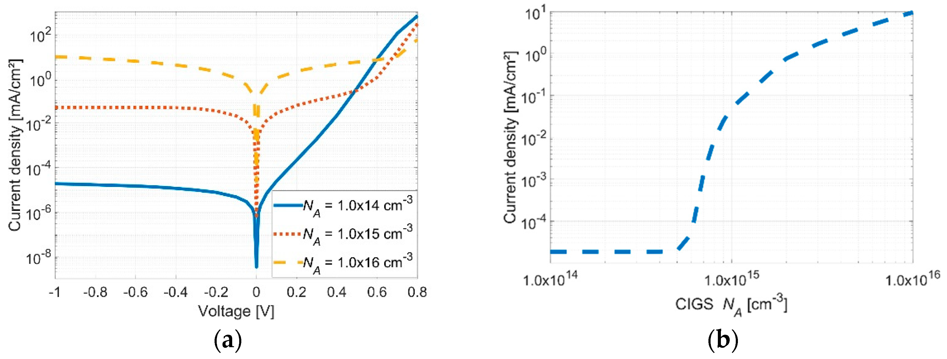
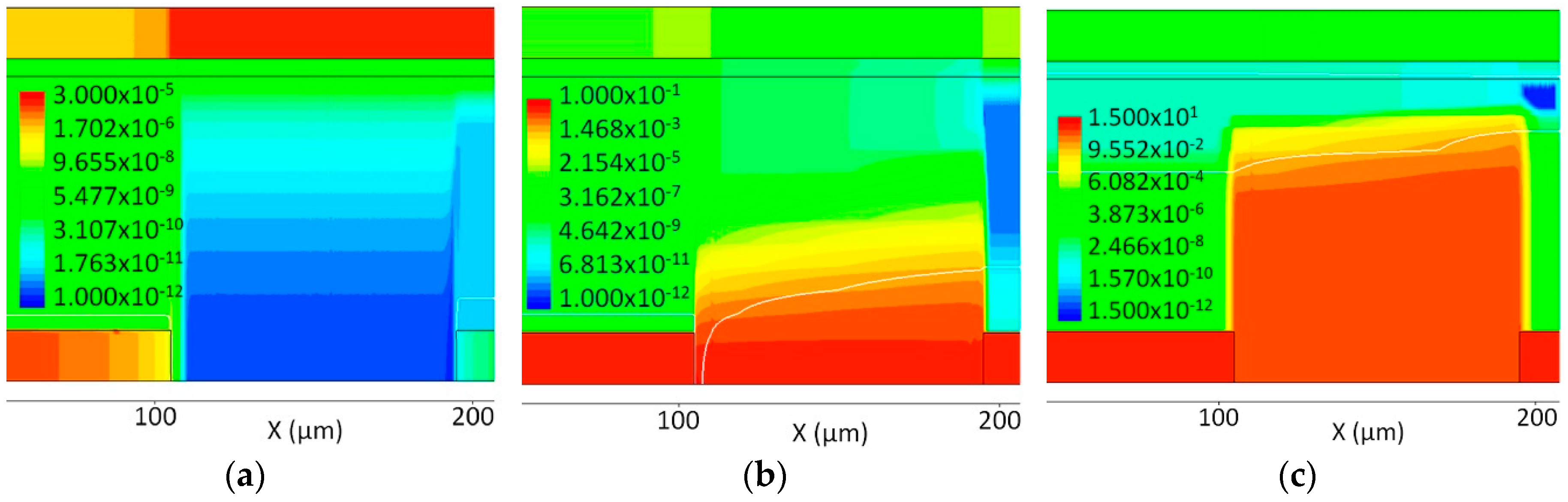
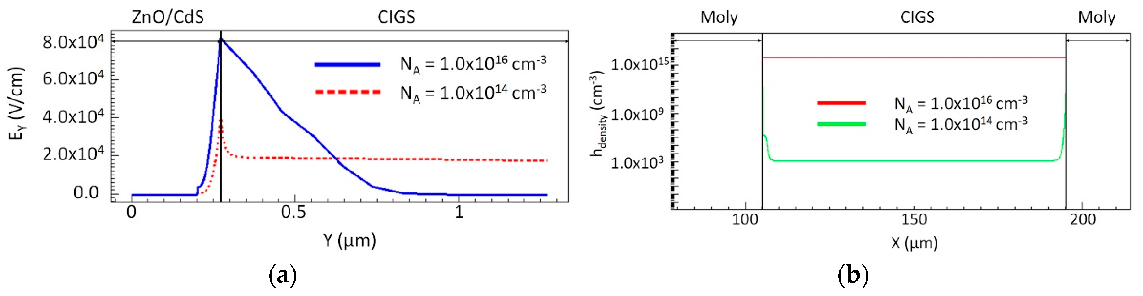
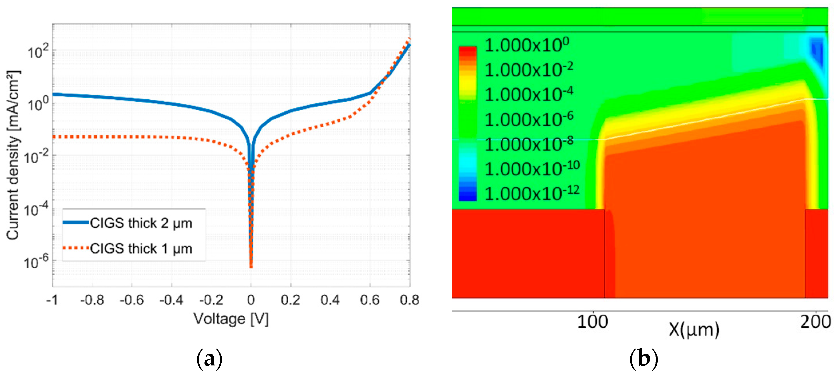
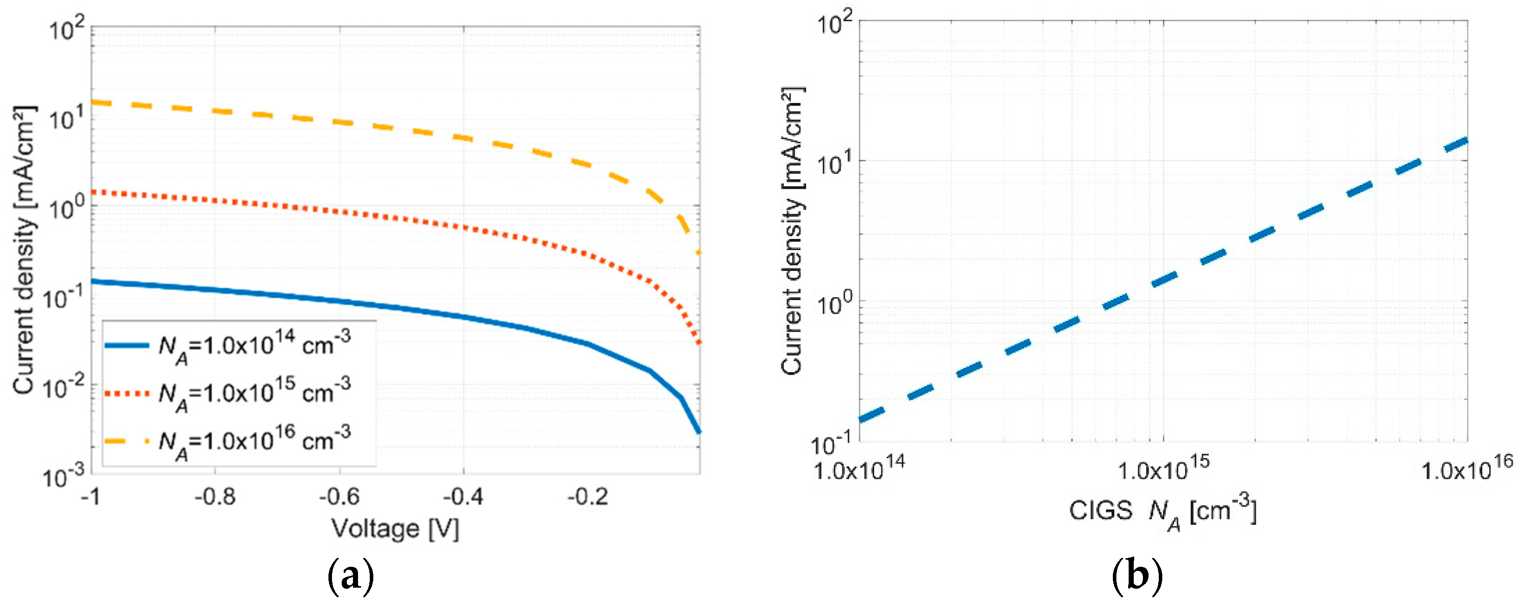
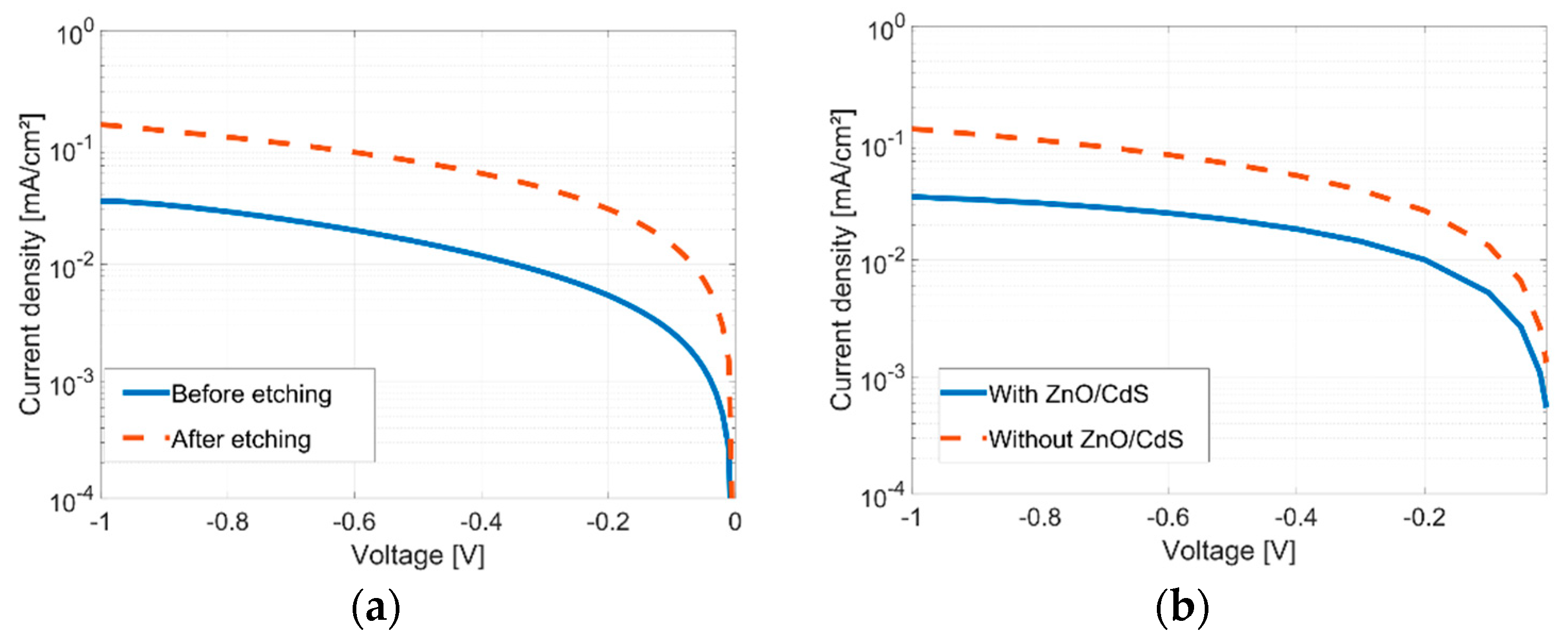
3.1. Results of the Simulations

Figure 2 presents the structure used for the first simulation, which is performed at 300 K. The results of this simulation are presented in Figure 4, with the JV-curve in the dark for varied NA values in the CIGS bulk. A nonlinear decrease of reverse current density with decreasing NA according to Figure 4b was observed. From the curves of Figure 4a it can also be deduced that the forward bias required to open the current path through the p–n junction decreases with NA. This bias could be related to the built-in voltage (Vbi) of the device [16], which is the height of the barrier due to the SCR.
Another interesting result that could be extracted from Figure 4a is the existence of a non-symmetric behavior between the forward and reverse bias regions for NA = 1014 cm−3. This can be explained by the fact that for lower values of NA, the non-linear diode behavior of the device starts to dominate over the linear one at lower positive biases compared to the case of higher CIGS dopings.
Figure 5 shows a 2D plot of the simulated current density. This result gives another hint regarding the transistor effect created by the SCR and the conductance through P1. If NA in CIGS decreases, the SCR extends into P1 and reduces the available space in the channel for the current flowing through it. To the contrary, when NA increases, the SCR shrinks to the junction, widening the channel.
As mentioned above, Vbi is reduced when NA decreases. It is possible to explain this behavior with the electric field inside the device across the p–n junction, [16]. In Figure 6a, a vertical cut of the vertical component of the electric field over the anode (see Figure 2a) for the extreme values of NA is presented. The electric field in the case of NA = 1016 cm−3 has a higher value at the CdS/CIGS interface than in the case of NA = 1014 cm−3. On the other hand, for NA = 1014 cm−3, the electric field in the CIGS bulk is constant, indicating full carrier depletion down to the contact, while in the case of NA = 1016 cm−3, the electric field in the CIGS bulk reduces linearly to 0, in support of the existence a quasi-neutral region with flat bands.
Further evidence of the effect of the SCR in the device is the absence of free carriers in the CIGS layer. These results belong to the simulation of the structure presented in Figure 2. In Figure 6b there is a representation of a horizontal cut between both contacts with the value of the free hole concentration. These curves correspond to values of NA = 1014 cm−3 and NA = 1016 cm−3. With lower NA, the concentration of free holes in P1 is also reduced, but not with a linear dependency on NA.
In the case of NA = 1014 cm−3, the concentration of free holes in P1 is 12 orders of magnitude lower than the value of NA, while in the case of NA = 1016 cm−3, the free hole density is in the same order of magnitude with the value of NA. This absence of free holes means that the hole current density between both contacts will also be reduced in the same proportion when a reverse bias is applied.
The thickness of the CIGS layer is another key parameter for the behavior of the device, as mentioned previously. The SCR extends into the CIGS layer, and if the width of the channel is sufficiently reduced, it is possible to close the path of the current through the P1 region. In Figure 7a we present a comparison between the current density for a 2 and a 1-µm thick CIGS layer. A particular emphasis on the current density in the P1-shunt for the device with a 2-µm thick CIGS layer NA = 1015 cm−3 is presented in Figure 7b.
If we compare the results presented in Figure 7b with those of Figure 5b, the SCR does not reach the bottom of P1 when the CIGS layer is thicker. In the structure with CIGS thickness of 1 µm, the SCR partially closes the path through P1, reducing the current density in reverse bias.
Figure 3a presents the structure of the second simulation with only CIGS/molybdenum layers, the latter divided by the P1 scribe. The temperature of the simulation was set at 300 K. A comparison between the JV-curves for different values of NA in CIGS can be seen in Figure 8a, whereas a curve of the variation of the current in reverse bias for values of NA between 1014 and 1016 cm−3 is shown in Figure 8b, where the current density increases linearly with the value of NA.

3.2. Experimental Results

It is possible to provide some evidence regarding the effect of the SCR in the reverse current of real devices. As mentioned before, if the ZnO/CdS layers are removed from the device via HCl etching, it will be possible to measure the JV-curve without the impact of the SCR. The results of the JV-measurement at 25 °C are shown in Figure 9, compared to simulation results from the models presented in Figure 2b and Figure 3b.
Both the experimental and simulated results show a similar behavior. When the ZnO/CdS layer was removed, the current density flowing between both contacts increased. As mentioned above, the simulation results relate this effect to the elimination of the SCR created due to the doping gradient between the n-type and p-type semiconductors. The semiconductor parameters of the CIGS sample used in the experiment are unknown, although it is possible to adjust the simulation parameters until a good compromise with experimental results is reached as indicated in Figure 9. A necessary reduction of hole and electron mobilities in order to fit experimental findings might be justified by the fact that the shunt path across P1 involves a lateral current transport across potential barriers due to grain boundaries, in agreement with [25]. The columnar nature of the grains leads to expect a higher number of grain boundaries in the horizontal direction (along the x-axis) compared to the vertical one (along the y-axis).

4. Discussion

The results of our work suggest a mechanism similar to the JFET simplified model presented in reference [9]. In our case, the equivalence of source and drain are both molybdenum contacts, and P1 is the channel. ZnO and CdS are part of the n-type gate material, which is directly connected to the drain. If a forward bias is applied, the current flows through the p–n junction instead of through the channel. Increasing or reducing the doping gradient between the p and n-type semiconductor layers affects the SCR in the device, and if this region is wide enough to close the channel, the P1 shunt conductance will be reduced.
This behavior is presented in Figure 4a, as the reverse current bias was significantly reduced when NA in CIGS is decreased below 1015 cm−3. Figure 4b provides further evidence of this transistor-like behavior, as the reverse bias current does not have a linear dependence with the applied bias. In fact, the reverse bias current is constant for values of NA lower than 5 × 1014 cm−3, as the SCR closes the path of the current through P1. If we increase this value, the current density in reverse bias increases exponentially as the SCR thickness is reduced and the path through P1 opens. After a certain value of NA in CIGS, in this case 1015 cm−3, the current density in reverse bias increases almost linearly. These results are in agreement with those presented in reference [11], in which decreasing the value of NA below 1015 cm−3 is shown to have no impact on the shunt resistance of the device. It is interesting to mention that a gallium gradient, which is present in highly efficient CIGS devices with bandgap grading [26], can also play a role in the transistor-like behavior. A depth-dependent gallium distribution may induce a doping gradient [27], which to certain extent could affect the width of the SCR, and therefore the transistor effect might not be present. For sake of simplicity in the modelling, this effect has not been considered in our simulations, but could be regarded as a topic for further work.
The decrease of Vbi is a side-effect of manipulating the value of NA. It should be considered carefully as it will also affect other parameters such as the open circuit voltage, the maximum power point, the fill factor and the efficiency. A good compromise between NA and CIGS thickness is required to decrease the P1 shunt while reducing the impact on these parameters.
Removing the ZnO/CdS layer provides further evidence of the impact of the SCR in the P1 shunt and the reverse current density of the device. In this situation, the SCR is not present, and the reverse current density depends only on NA; thus, the transistor effect is not present in the behavior of the device. In Figure 8b, the reverse current density increases proportional to NA; in contrast with the results presented in Figure 4b. This increase in the reverse bias current is also presented in reference [18], in which the elimination of the SCR is considered to be the main reason behind this behavior.
This elimination of the transistor-like behavior is made plausible in the experimental results and the simulation of Figure 9. Etching away the ZnO/CdS layer increases the reverse current density. This increase may vary depending on the width of the SCR and the thickness of the CIGS layer. The results of our simulations are in agreement with experimental findings.

5. Conclusions

Based on 2D simulation results of CIGS cells with monolithic interconnects we proposed a mechanism that affects the P1 shunt, and consequently, the Ohmic behavior of the device. As has been discussed in this contribution, this mechanism has similarities with the behavior of a p-type JFET transistor device. According to this model, CIGS in P1 is the p-type channel in the device. As has been shown in the simulations, varying the thickness and the doping of CIGS, the width of the channel can be modulated, and therefore the current flowing in P1. Reducing NA extends the SCR into the P1 interconnect. This means that the channel width is narrowed leading to a decreased shunt conductance. Experimental evidence was also provided to support the validity of the simulations. JV-measurements before and after etching the ZnO/CdS layer showed that when the n-type semiconductor was removed, the SCR and the transistor behavior were eliminated. The simulation results of a model with and without the ZnO/CdS layers support qualitatively the proposed mechanism.

Author Contributions

Conceptualization, R.V.L. and T.W.; Methology, R.V.L. and T.W.; Project Administration, T.W.; Supervision, D.F.M. and T.W.; Investigation, R.V.L.; Writing—Original Draft, R.V.L.; Writing—Review and Editing, T.W., T.L., D.M. and D.F.M.

Funding

This research was financed by the Federal Ministry for Economic Affairs and Energy of Germany under the proCIGS project (No. 0324070).

Acknowledgments

We would like to thank the Ulm University of Applied Sciences and IES-UPM (Instituto de Energía Solar, Universidad Politécnica de Madrid) for their support in this project.

Conflicts of Interest

The authors declare no conflict of interest.

References

  1. Jackson, P.; Wuerz, R.; Hariskos, D.; Lotter, E.; Witte, W.; Powalla, M. Effects of heavy alkali elements in Cu(In,Ga)Se2 with efficiencies up to 22.6%. Phys. Status Solidi RRL Rapid Res. Lett. 2016, 10, 583–586. [Google Scholar] [CrossRef]
  2. Green, M.A.; Hishikawa, Y.; Dunlop, E.D.; Levi, D.H.; Hohl-Ebinger, J.; Ho-Bailie, W.A. Solar cell efficiency tables (version 52). Prog. Photovolt. Res. Lett. 2018, 427–436. [Google Scholar] [CrossRef]
  3. Green, M.A.; Emery, K.; Hishikawa, Y.; Warta, W.; Dunlop, E.D. Solar cell efficiency tables (version 48). Prog. Photovolt. Res. Appl. 2016, 24, 905–913. [Google Scholar] [CrossRef] [Green Version]
  4. Yang, S.; Lin, K.-M.; Lee, W.-C.; Lo, W.-S.; Chen, C.-H.; Wu, J.-L.; Chiang, C.-Y.; Wu, C.-H.; Sun, Y.-L.; Lo, H.; et al. Achievement of 16.5% total area efficiency on 1.9 m2 CIGS modules in TSMC solar production line. In Proceedings of the IEEE 42nd Photovoltaic Specialist Conference (PVSC), New Orleans, LA, USA, 14–19 June 2015. [Google Scholar] [CrossRef]
  5. Contreras, M.A.; Egaas, B.; Ramanathan, K.; Hiltner, J.; Schwartzlander, A.; Hasoon, F.; Noufi, R. Progress towards 20% efficiency in Cu(In,Ga)Se2 polycristalline thin-film solar cells. Prog. Photovolt. Res. Appl. 1999, 7, 311–316. [Google Scholar] [CrossRef]
  6. Scheer, R.; Schock, H.-W. Chalcogenide Photovoltaics: Physics, Technologies and Thin Film Devices; Wiley-VCH Verlag GmbH & Co.: Weinheim, Germany, 2011; pp. 9–127. [Google Scholar]
  7. Portmans, J.; Arkhipov, V. Thin Film Solar Cells: Fabrication, Characterization and Applications; John Wiley & Sons: Chichester, UK, 2006; pp. 237–275. [Google Scholar]
  8. Brecl, K.; Topič, M.; Smole, F. A detailed study of monolithic contacts and electrical losses in a large-area thin-film module. Prog. Photovolt. Res. Appl. 2015, 13, 297–310. [Google Scholar] [CrossRef]
  9. Yoon, J.H.; Park, J.K.; Kim, W.M.; Lee, J.; Pak, H.; Jeong, J.H. Characterization of efficiency-limiting resistance losses in monolythically integrated Cu(In,Ga)Se2 solar modules. Sci. Rep. 2015, 5, 7690. [Google Scholar] [CrossRef] [PubMed]
  10. Neamen, D.A. Semiconductor Physics and Devices: Basic Principles, 4th ed.; McGraw-Hill: New York, NY, USA, 2012; pp. 571–611. [Google Scholar]
  11. Schubbert, C.; Eraerds, P.; Richter, M.; Parisi, P.; Riedel, I.; Dalibor, T.; Palm, J. Performance ratio study based on a device simulation of a 2D monolithic interconnected Cu(In,Ga)(Se,S)2 solar cell. Sol. Energy Mater. Sol. Cells 2016, 157, 146–153. [Google Scholar] [CrossRef]
  12. Sozzi, G.; Pignoloni, D.; Menozzi, R.; Pianezzi, F.; Reinhard, P.; Bissig, B.; Buecheler, S.; Tiwari, A.N. Designing CIGS solar cells with front-side point contacts. In Proceedings of the IEEE 42nd Photovoltaic Specialist Conference (PVSC), New Orleans, LA, USA, 14–19 June 2015. [Google Scholar] [CrossRef]
  13. Park, J.; Shin, M. Numerical optimization of gradient bandgap structure for CIGS solar cells with ZnS buffer layer using Technology Computer-Aided Design simulation. Energies 2018, 11, 1785. [Google Scholar] [CrossRef]
  14. Movla, H. Optimization of the CIGS based thin-film solar cells: Numerical simulations and analysis. Optik 2014, 125, 67–70. [Google Scholar] [CrossRef]
  15. Synopsys. Available online: https://www.synopsys.com/silicon/tcad.html (accessed on 3 December 2018).
  16. Sze, S.M.; Ng, K.K. Physics of Semiconductor Devices, 3rd ed.; John Wiley & Sons: Hoboken, NJ, USA, 2007; pp. 79–124. [Google Scholar]
  17. Li, S.; Fu, Y. 3D TCAD Simulation for Semiconductor Processes, Devices and Optoelectronics; Springer: New York, NY, USA, 2012; pp. 41–80. [Google Scholar]
  18. Lavrenko, T.; Vidal Lorbada, R.; Muecke, D.; Walter, T.; Plesz, B.; Schaeffler, R. Towards an improved understanding of CIGS thin film solar cells. In Proceedings of the 33rd European Photovoltaic Solar Energy Conference and Exhibition, Amsterdam, The Netherlands, 25–29 September 2017. [Google Scholar] [CrossRef]
  19. Powalla, M.; Cemernjak, M.; Eberhardt, J.; Kessler, F.; Kniese, R.; Mohring, H.D.; Dimmler, B. Large-area CIGS modules: Pilot line production and new developments. Sol. Energy Mater. Sol. Cells 2006, 90, 3158–3164. [Google Scholar] [CrossRef]
  20. Westin, P.O.; Zimmermann, U.; Edoff, M. Laser patterning of P2 interconnect via in thin-film CIGS PV modules. Sol. Energy Mater. Sol. Cells 2008, 92, 1230–1235. [Google Scholar] [CrossRef]
  21. Heise, G.; Boerner, A.; Dickmann, M.; Englmaier, M.; Heiss, A.; Kemnitzer, A.; Konrad, J.; Moser, R.; Palm, J.; Vogt, H.; et al. Demonstration of the monolithic interconnection on CIS solar cells by picosecond laser structuring on 30 by 30 cm2 modules. Prog. Photovolt. Res. Appl. 2015, 23, 1291–1304. [Google Scholar] [CrossRef]
  22. Fields, J.D.; Dabney, M.S.; Bollinger, V.P.; van Hest, M.F. Printed monolithic interconnects for photovoltaic applications. In Proceedings of the IEEE 40th Photovoltaic Specialist Conference (PVSC), Denver, CO, USA, 8–13 June 2014. [Google Scholar] [CrossRef]
  23. Mack, P.; Ott, T.; Walter, T.; Hariskos, D. Optimization of reliability and metastability of CIGS solar cell parameters. In Proceedings of the 25th European Photovoltaic Solar Energy Conference and Exhibition, Valencia, Spain, 6–10 September 2010. [Google Scholar] [CrossRef]
  24. Ott, T.; Lavrenko, T.; Walter, T.; Schaeffler, R.; Fetch, H.-J. On the importance of the back contact for Cu(In,Ga)Se2 thin film solar cells. In Proceedings of the 29th European Photovoltaic Solar Energy Conference and Exhibition, Amsterdam, The Netherlands, 22–26 September 2014. [Google Scholar] [CrossRef]
  25. Abou-Ras, D.; Schmidt, S.S.; Schaefer, N.; Kavalakkatt, J.; Rissom, T.; Unold, T.; Mainz, R.; Weber, A.; Kirchartz, T.; Sanli, E.S.; et al. Compositional and electrical properties of line and planar defects in Cu(In,Ga)Se2 thin films for solar cells—A review. Phys. Status Solidi Rapid Res. Lett. 2016, 10, 363–375. [Google Scholar] [CrossRef]
  26. Dullweber, T.; Hanna, G.; Shams-Kohali, W.; Schwartzlander, A.; Contreras, M.A.; Noufi, R.; Schock, H.W. Study of the effect of gallium grading in Cu(In,Ga)Se2 with efficiencies up to 22.6%. Thin Solid Films 2000, 361, 478–481. [Google Scholar] [CrossRef]
  27. Frisk, C.; Platzer-Bjoerkman, C.; Olsson, J.; Szaniawski, P.; Waetjen, J.T.; Fjaellstroem, V.; Salomé, P.; Edoff, M. Optimizing Ga-profiles for highly efficient Cu(In,Ga)Se2 thin-films in simple and complex defect models. J. Phys. D Appl. Phys. 2014, 47, 485104. [Google Scholar] [CrossRef]
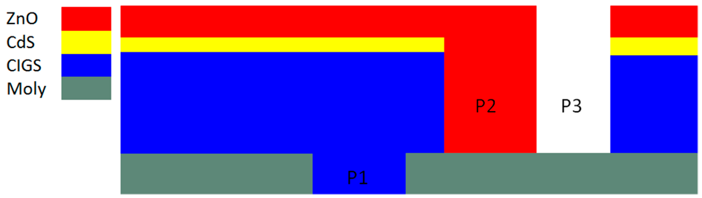
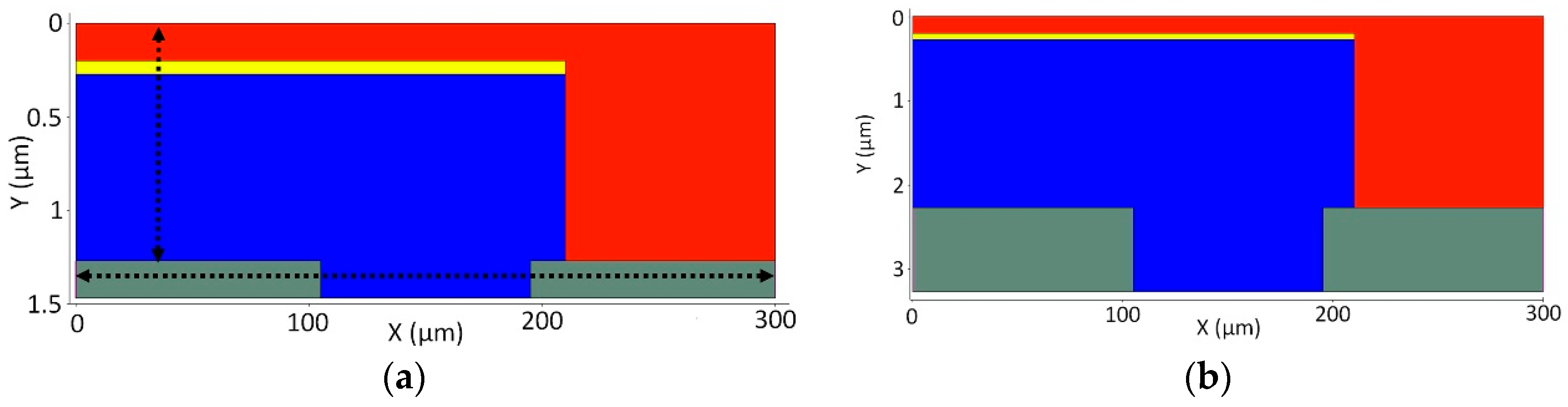
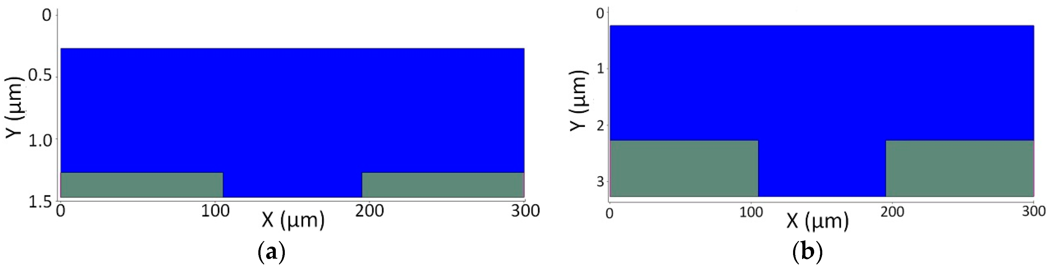
Figure 1. Schematic of Cu(In,Ga)Se2 (CIGS) device with ZnO/CdS/CIGS/Moly and P1, P2, P3 scribes.
Coatings 09 00128 g001
Figure 2. (a) Device structure with reduced CIGS and molybdenum thickness (1 and 0.2 µm, respectively), the vertical and horizontal lines indicate the positions of the vertical and horizontal cuts of 2D results, respectively; (b) device structure with extended CIGS and molybdenum thickness (2 and 1 µm, respectively).
Coatings 09 00128 g002
Figure 3. Device structure without ZnO/CdS layers. (a) CIGS and molybdenum thickness of 1 and 0.2 µm, respectively; (b) CIGS and molybdenum thickness of 2 and 1 µm, respectively.
Coatings 09 00128 g003
Figure 4. (a) Semilog JV-curve of the structure for varied values of NA; (b) Current density at 1 V reverse bias for varied values of NA.
Coatings 09 00128 g004
Figure 5. 2D representation of the current density flowing through the P1-shunt under a reverse bias of 1 V between anode and cathode for CIGS with: (a) NA = 1014 cm−3; (b) CIGS NA = 1015 cm−3; (c) NA = 1016 cm−3. The color scale of each plot is in (mA/cm2).
Coatings 09 00128 g005
Figure 6. (a) Vertical cut (see Figure 2a) of the Y-component of the electric field (Ey) with NA = 1016 cm−3 and 1014 cm−3 under a bias between anode and cathode of 0 V; (b) Horizontal cut (see Figure 2a) of the free hole density between both molybdenum contacts for NA = 1016 and 1014 cm−3.
Coatings 09 00128 g006
Figure 7. (a) JV-curve in the dark for the structures with 2 and 1 µm CIGS layer thickness, respectively and NA = 1015 cm−3; (b) 2D plot of the current density flowing through P1 in the structure with 2 µm CIGS and 1 µm molybdenum thicknesses under reverse bias of 1 V, the color scale is in mA/cm2.
Coatings 09 00128 g007
Figure 8. (a) Dark JV-curves of the device without ZnO/CdS for values of NA between 1014 cm−3 to 1016 cm−3; (b) Current density vs. NA under a reverse bias of 1 V between both contacts.
Coatings 09 00128 g008
Figure 9. (a) JV-curve in reverse bias of the device before and after etching the ZnO/CdS layers; (b) Simulated JV-curves in reverse bias of the structures presented in Figure 2b (with ZnO/CdS layers) and Figure 3b (with no ZnO/CdS layer) with NA = 3 × 1014 cm−3. Electron and hole mobilities are reduced to 0.25 and 0.5 cm2/V·s, respectively, to fit the experimental curves.
Coatings 09 00128 g009
Table 1. Key parameters of the functional layers with the dimensions of scribes and dead area.
LayerND (cm−3)NA (cm−3)Χ (eV)μe (cm2/V·s)μh (cm2/V·s)Εg (eV)Thickness (μm)ScribeWidth (μm)
ZnO10204.650203.50.2P190
CdS10174.450202.50.05P290
CIGS1014–10164.650201.21.00–2.00Dead area200
Moly0.20–1.0Total300

