Article

Luminescence of CsI and CsI:Na Films under LED and X-ray Excitation

1
Department of Physics, Fu Jen Catholic University, No.510 Zhongzheng Rd., Xinzhuang Dist., New Taipei City 24205, Taiwan
2
Graduate Institute of Applied Science and Engineering, Fu Jen Catholic University, No. 510 Zhongzheng Rd., Xinzhuang Dist., New Taipei City 24205, Taiwan
*
Author to whom correspondence should be addressed.
Coatings 2019, 9(11), 751; https://doi.org/10.3390/coatings9110751
Submission received: 27 October 2019 / Revised: 10 November 2019 / Accepted: 11 November 2019 / Published: 13 November 2019
(This article belongs to the Special Issue Functional Thin Films: Design, Fabrication and Applications)

Abstract

:
In this study, we investigated the luminous properties of undoped cesium iodide (CsI) and Na-doped CsI (CsI:Na) films deposited by thermal vacuum evaporation and treated with different substrate temperatures, post-annealing temperatures, and deposition rates. The quality of the deposited films was evaluated by their XRD pattern, SEM cross-section/surface morphologies and UV/X-ray luminescence, the spectra of which were used to derive the luminescence mechanism of the deposited films. The 310 nm luminescence demonstrates that the exciting light arises from the electron–hole recombination through the self-trapped exciton (STE) process, which is characteristic of the host polycrystalline CsI. The broad-band luminescence from ~400 to 450 nm demonstrates the other electron–hole recombination between the new energy states created by doping Na in the forbidden gap of CsI. When we deposited higher quality films at a substrate temperature of 200 °C, the undoped CsI films showed preferred crystal orientation at (200), and the CsI:Na films co-evaporated by 1 wt.% NaI at (310) and had the highest UV/X-ray luminescence.

1. Introduction

Undoped cesium iodide (CsI) has been widely used for efficient scintillation [1,2] because cesium (Cs) and iodide (I) have high atomic numbers and large stopping power [3,4]. It strongly absorbs UV light, X-rays, and gamma-rays and presents very fast luminescence emission on the order of 10 ns [5,6,7,8]. When excited by a higher-energy photon, some of the electrons in the valence band jump over the forbidden gap to the conduction band. In the de-excitation process of the larger width of the forbidden gap, the photons emit UV light in the energy region of 3.7 to 4.3 eV [9,10]. An energy state is generated in the forbidden gap by adding sodium (Na) or thallium (Tl) dopant to the CsI film to convert X-rays and gamma rays into visible light and to increase the luminescent effect [11,12]. Thus, the excited CsI:Na films emit a visible blue light of about 3 eV (λ = 431 nm) that shows recombination of the primary emission of CsI disturbed by the dopants [9,11].
The luminescence properties and preferred crystal orientations are different because of the different fabrications and thicknesses of the films [13]. In our research, the problem of different crystal orientations has also plagued us for many years [14,15,16,17]. However, the complicated preferred peaks for CsI crystal are (110), (200), (211), (220), (310), (222), and (321). The lattice planes corresponding to the CsI powder are (110), (200), (211), (220), (310), (222), and (321) [18,19].
In our previous studies, we successfully mixed CsI powder with a small amount of NaI co-evaporated by thermal vacuum deposition because the boiling point of NaI 1304 ± 5 °C is near that of CsI 1277 ± 5 °C [19,20]. However, moisture can significantly alter the alkaline halide structure [14]. The luminescent light from the film then spreads and broadens, resulting in a reduction in the resolution of the image used as an X-ray image converter [21]. Furthermore, the nanoparticles of NaI are more hygroscopic in the air than other alkali halides. An anti-moisture process after the deposition process of CsI:Na film is necessary because the hygroscopic nanoparticles remarkably decrease the luminescence scintillation and generate cracks in the cylindrical structure [9,12,22,23,24,25]. In previous studies, the protective SiO2, Al, and parylene-N layers subsequently deposited on the CsI or CsI:Na film in the same vacuum chamber was investigated, respectively [14,15,16,17,19]. The parylene-N layer can protect the films as a columnar structure. In this paper, we studied the scintillation mechanism of CsI:Na films from their optical and structural properties.
The nature of the inherent luminescence and the mechanism of CsI have been studied since the twentieth century [26,27,28]. The luminescence process is due to the attenuation of two types of self-capturing excitons (STE) [5,9,10,27]. One is the on-center STE, the electrons of which were captured at Vk- centers at room temperature. The other is the off-center STE with F-and H-center pairs formed by the molecular ion I2 at a temperature of less than 100 K [29]. Adiabatic potential energy surface (APES) indicates the variation of the luminescence spectra with temperatures resulting from the re-distribution of the electron population between on- and off-center STEs. The Onsager mechanism has also been used to describe the temperature dependence of the scintillation light [30,31]. The CsI and CsI:Na scintillators emit photons with a wavelength between 280 and 350 nm in the de-excitation process, according to the evidence of some investigations summarized in Table 1. In spite of the higher excitation energy of Am-241 gamma rays [32] or the lower excitation energy of 277 nm UV light [33], the emission of STE was still within the range 285 to 435 nm. This study shows that the wavelength of the STE with interference from the sodium dopant is longer than that of the undisturbed STE because sodium activators produce energy levels after Na doping in CsI film. That is discussed in Section 3.4.
Furthermore, the separating column structure of CsI film, which suppresses lateral light scattering due to the total internal reflection from their boundary surfaces, can be used as light guides for the scintillation light generated by X-ray excitation to increase the spatial resolution of the X-ray image [36]. In this study, the higher deposition rate also promotes the formation of columnar structure and higher packing density of the films. The deposited films preferably have not only a columnar structure but also moisture resistance [37].

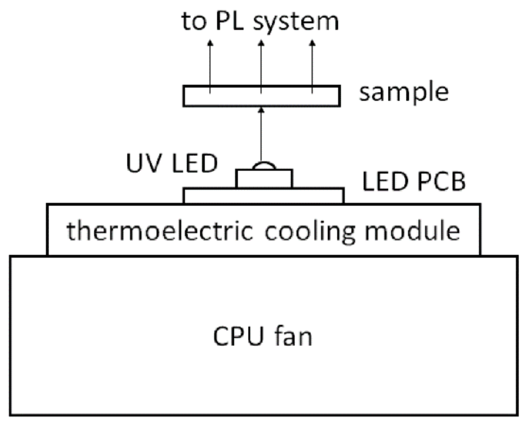
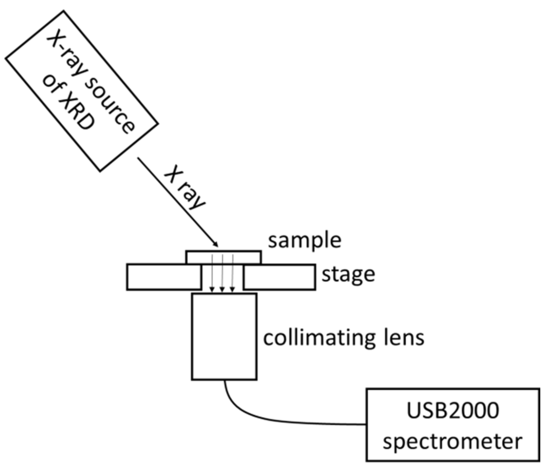
2. Materials and Methods

The CsI and CsI:Na films can be evaporated out of a box-type molybdenum boat (15 × 20 × 70 mm3) with a perforated cover. The undoped CsI powder or its mixture with 0.5, 1, or 2 wt.% NaI powder, with a total weight of about 50 g, was placed in the boat. Before the vacuum, thermally resistant evaporation, B270 glasses and silicon wafers were cleaned with alcohol in an ultrasonic bath, blow-dried with dry nitrogen gas, and then placed in a substrate holder positioned approximately 25 cm above the boat.
The chamber was evacuated to a base pressure of 4 × 10⁻⁶ Torr by using a diffusion pump. The molybdenum boat was preheated with a current of about 50 A with a 12 VAC power supply for about 30 min to outgas the evaporated material. The moisture released from the mixture of deposited CsI and NaI materials reduced the oxygen composite in the films. The vacuum pressure lightly increased during the preheating process. The outgas process finished when the pressure decreased again to the base pressure with continuous pumping. The molybdenum boat was then heated using an electric current of about 200 A to deposit the films.
We divided the experimental results into four parts with thicknesses ranging about 5 to ~176 μm and at deposition rates ranging from 3 to 110 nm/sec, as shown in Table 2. The thicknesses were about 15 μm in Part 4, as the substrate platform was rotated during the deposition, and the evaporation source was about 100 mm away from the axis of rotation to achieve thickness uniformity.
These as-deposited films were labeled with CsI:Na(x%), where x (values from 0.5, 1, to 2) is the weight percentage (wt.%) of the amount of co-evaporated material in NaI. The substrate temperature (Ts) or post-annealing temperature (Tp) in the vacuum was room temperature (RT) to 300 °C. The post-annealing process increased the temperature rate by about 15 °C/min, and we kept the final temperature for one hour and then naturally cooled it to room temperature.
By preventing the hygroscopic CsI:Na films from absorbing the moisture in the atmosphere, we sequentially evaporated a parylene-N layer on the films in the same vacuum chamber, using the thermal decomposition method. A homemade ceramic evaporator boat 10 × 10 × 40 mm3 in size was covered with a perforated molybdenum foil [15]. Before the pumping of the vacuum chamber, the parylene-N dimer ~5 g was transferred into the ceramic evaporator boat. During the thermal decomposition process, the dimer was sublimated by thermal radiation from the perforated Mo foil heated by a high electric current of 100 A and was pyrolyzed into a monomer [38,39] through the small holes of the foil. The monomer vapor formed a polymer on the surface of the CsI:Na film. The polymer layer was deposited at about 1 μm thickness at a rate of ~0.7 nm/sec and a working pressure of 8 × 10⁻⁴ Torr.
The samples were investigated by a Fourier transform infrared (FTIR) spectrometer Perkin-Elmer 100 (Perkin Elmer, Inc., Waltham, MA, USA) from 3250 to 3750 cm−1 to measure the moisture absorption on the films. Morphologies of the surfaces and cross-sections of the films were observed by a scanning electron microscope (SEM) Hitachi S-3400N (Hitachi Ltd., Chiyoda-ku, Tokyo, Japan). An X-ray diffractometer Rigaku Multiflex (Rigaku Co., Spring, TX, USA) was used to obtain the sample’s X-ray diffraction (XRD) patterns. The luminescence properties of the films were measured by using a PL system with a 275 nm UV LED (LG Innotek Co., Jung-gu, Seoul, Korea) built in-house, as shown in Figure 1.
The LED source was driven by the forward voltage of 8 VDC and cooled down by a thermoelectric cooling module with a CPU fan to keep the operating temperature less than 60 °C. The UV LED provides a flux of 10 mW, more radiant than that of a PL (photoluminescence) system derived by a monochromator, and its FWHM of 12.0 nm is narrower than that of a general UV light source. The X-ray luminescence spectra of the samples were collected using a homemade X-ray excitation luminescence system, as shown in Figure 2. We put the sample on the XRD hollow stage of the X-ray diffractometer Rigaku Multiflex. The sample film was placed face down on the stage. The incident angle of the irradiating X-ray was about 45°. The emitting luminescence from the film was collected by a UV collimating lens to be analyzed using a spectrometer USB2000 (Ocean Optics, Inc., Largo, FL, USA).

3. Results and Discussion

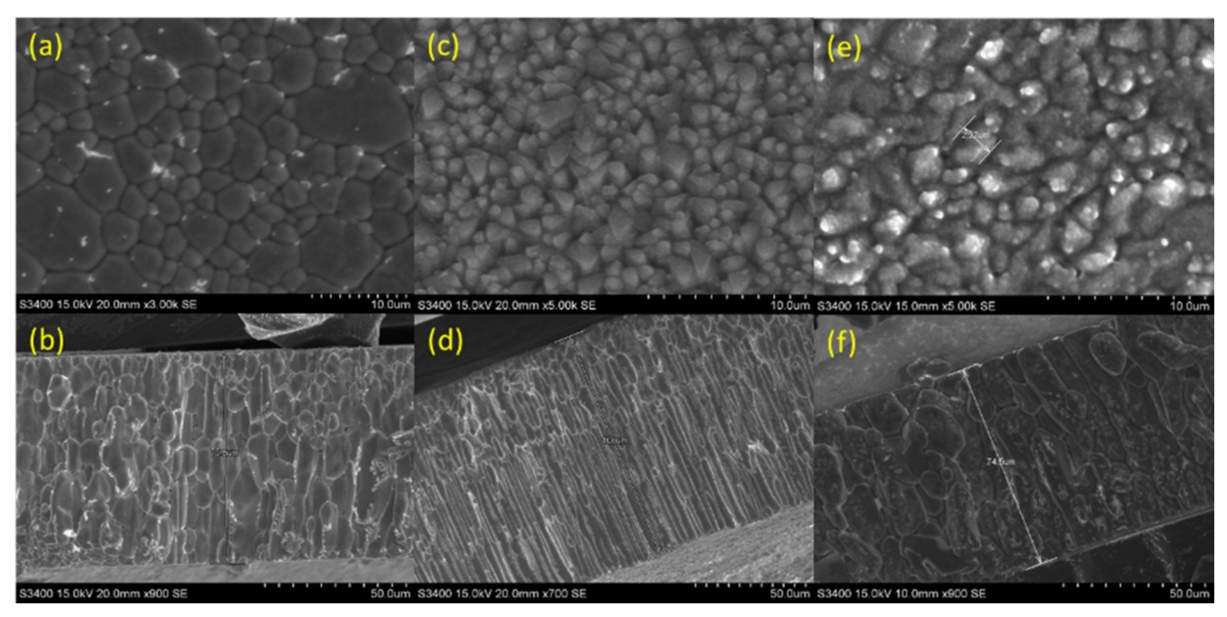
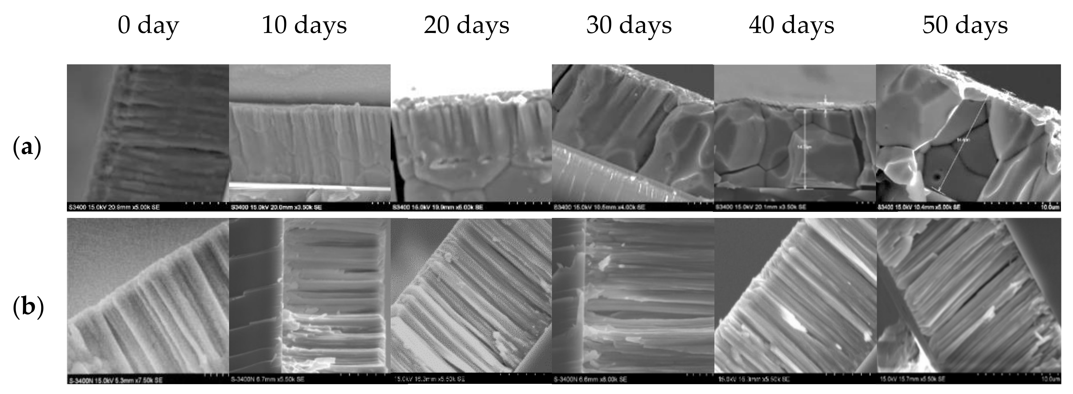
3.1. Columnar Structure

In this study, the heating substrate temperature (Ts) is an important factor that determines the orientation of the polycrystalline film. The very clear nucleation of the CsI polycrystalline in the orientation results from low surface energy during deposition [12,23]. The CsI films were deposited at <0.1 mTorr without a heating substrate. Its cross-section as shown in Figure 3a illustrates the complex fabric structure Zone T of the Thornton model at Ts/Tm ratio = 0.35, where Tm is the melting point of 600 °C (894 K) of the CsI material [40]. With the increase in Ts to 200 °C (473 K), the cross-section in Figure 3c shows the simpler columnar structure as Zone II at Ts/Tm ratio = 0.53. The complex fabric structure having a saw-tooth multi-layer surface shown in Figure 3b is rougher than the simple structure having a grainy texture shown in Figure 3d.
Cesium iodide is the ionic compound of cesium and iodine and a deliquescent material. When the film reacts with moisture in the air, its luminescence property greatly decreases. Moreover, many cracks on the film’s surface enhance moisture absorption due to capillary action. The cracks result from the film’s stress, as shown by XRD in Section 3.3.3. We found that various deposited materials, such as SiO2, Al, and parylene-N, act as a protective layer against moisture. Large cracks appear on the surface, as shown in Figure 4a, because of the reduced flexibility of the inorganic SiO2 film. The aluminum metal film has good ductility but fills the cracks incompletely, as shown in Figure 4b. The cracks hardly appear on the protective layer of parylene-N shown in Figure 4c. The moisture resistance of the aluminum layer is less than that of the parylene-N layer, as shown in Section 3.2.
The Na dopant strongly influences the CsI structure, inhibits the poly-crystallinity, and becomes more hygroscopic. Figure 5 shows that the CsI:Na films have various columnar structures and surface morphologies with various amounts of Na dopant. The Na dopant of CsI:Na(0.5%) has apparently changed the surface shown in Figure 5a and cross-section shown in Figure 5b. CsI:Na(1%) (Figure 5c) exhibits an obvious poly-crystalline structure compared with the smooth CsI:Na(0.5%) (Figure 5a) and the condensing CsI:Na(2%) (Figure 5e). Moreover, CsI:Na(1%) (Figure 5d) exhibits a columnar structure more pronounced than that of CsI:Na(0.5%) (Figure 5b) and CsI:Na(2%) (Figure 5f). The aggregate structure of CsI:Na(2%) results from more moisture penetrating the columnar structure.

3.2. Moisture Absorption

Figure 6 shows the composites measured by an energy dispersive spectrometer (EDS). The undoped CsI film not only has equal amounts of cesium (40.31 at.%) and iodide (39.53 at.%) but also has oxygen (5.46 at.%), as shown by the absorbed moisture [15]. During the thermal deposition process, the combination ratio of the two atoms of the CsI film remains almost the same. The 5.46 at.% oxygen may show the hygroscopicity of the CsI film. It also shows that the CsI film contains a CsIO3 species. Cesium atoms may react with H2O that comes from the deposited powder or the deposition vacuum chamber, as shown by the XRD pattern in the next section.
Figure 7a shows the forming block aggregation structure of the CsI films protected by the ~1 µm aluminum layer when exposed to air from 1 to 50 days. The CsI films protected by the parylene-N layer remain in the columnar structure of ~3 μm and have a thickness of ~14 μm as shown in Figure 7b. Parylene-N exhibits hydrophobic surface properties, relatively low gas permeability, transparency at wavelengths above 400 nm, and relatively high tensile strength in the temperature range of −200 to 200 °C. The high compliance and stability properties make parylene-N an ideal protective layer for CsI film affected by moisture [41]. However, a porosity column structure of the CsI films shown in Figure 7b still absorb moisture, which can be measured by FTIR because of the ~3500 cm−1 infrared absorption by the water in the film. In Figure 8a, T0 is the transmittance value of the film containing no moisture between the two peaks of the transmittance curve, and T is the lowest transmittance at ~3500 cm−1 of the film containing moisture.
The density of water (pw) in the film can be determined by the following correlation formula [42,43]:
p w = ln ( T 0 / T ) α w d f
where αw is the water vapor absorption rate of 1.27 × 104 cm−1 at ~3500 cm−1, and df is the film thickness. Figure 8a shows the FTIR spectrum of the undoped CsI film exposed to air for 5 days. The packing density (p) is the density of the film at the ratio of the volume occupied by the bulk film to the total film’s volume, which can be expressed as follows:
p = 1 p w = 1 ln ( T 0 / T ) α w d f
Figure 8b shows that the packing density is stable at 0.98847 ± 0.000419 on average when the sample is exposed to air for 5 days. In our previous study, the packing density of the CsI film without a protective layer quickly decreases to 0.745 for 5 days [20]. That is, the parylene-N layer successfully prevents moisture intrusion of the CsI film. It can be proved by XRD in Section 3.3.2 that less Cs2O is formed on the surface of the element cesium oxidized after exposure to the air [44].

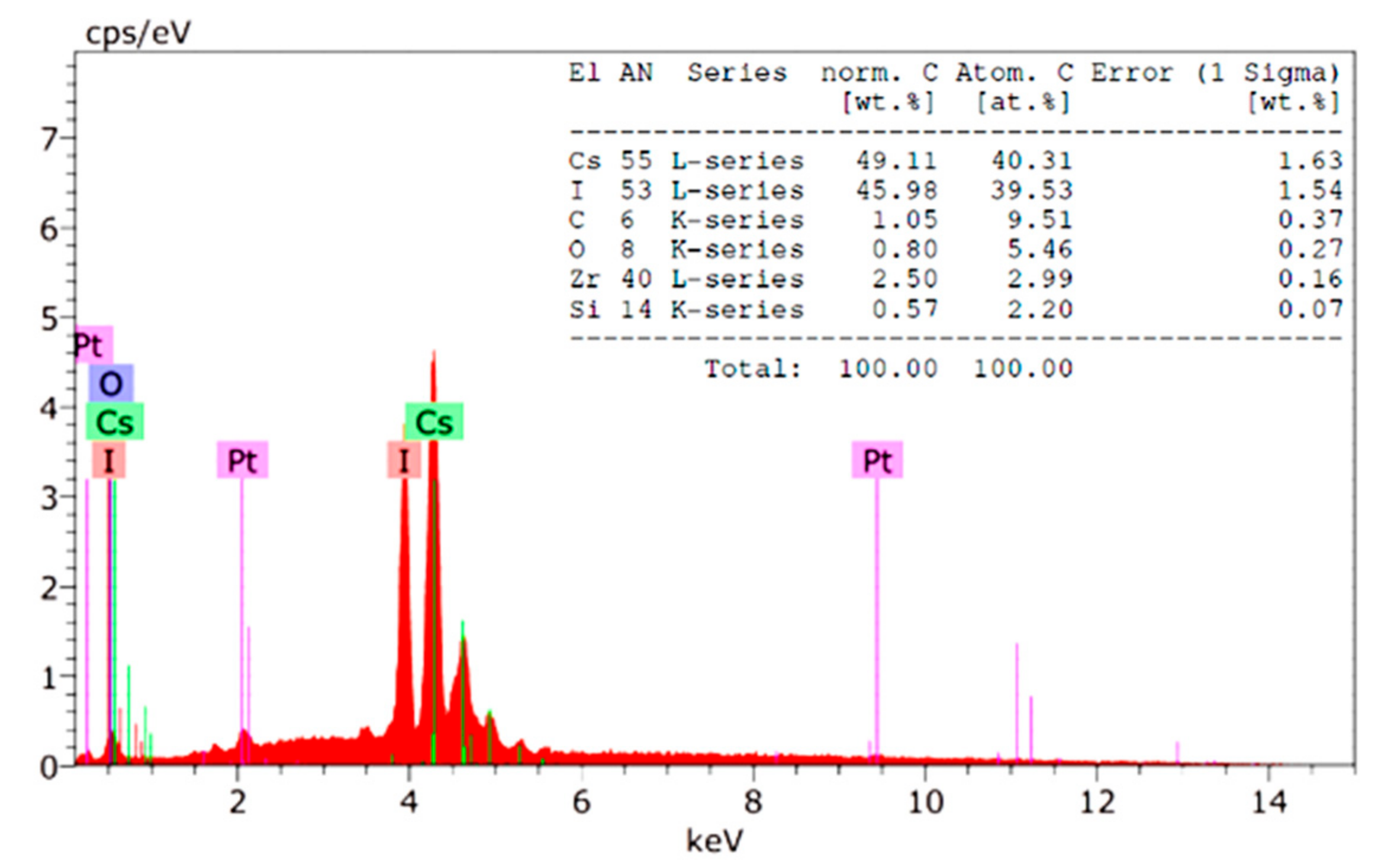
3.3. X-ray Diffraction Affected by Heat, Thickness, and Na Dopant

The CsI powder exhibits complex crystalline orientations along the (110), (200), (211), (220), (310), (222), and (321) planes [17]. The primary crystalline orientations are at (110) [18]. CsI and CsI:Na films have many crystalline orientations. Table 3 shows the primary crystalline orientations for distinguishing the polycrystalline properties of the films. A decrease in the number of crystalline orientations regularly occurs in the deposition process. Triloki et al. investigated the CsI films deposited at thicknesses of 4 to 500 nm from the single crystalline orientation (110) to the complex crystalline orientations of (110), (200), (211), (220), and (321). The thickness clearly affects the crystalline orientations of the film [44,45].

3.3.1. XRD of Undoped CsI Film

In our studies, the CsI deposited films with thicknesses much larger than 500 nm exhibit different crystalline orientations of (110), (200), (211), and (310) according to the deposition process. From the experimental data of Part 1, the primary peak (200) appears without heating, at Tp from 100 to 300 °C, and at Ts 100 and 300 °C conditions. The primary peak (110) only shows at a lower thickness of 5 μm at Ts 150–250 °C in our studies. With the increase in the CsI thickness to 8 μm in Part 2, the primary peak tends to (200) without heating and in the Tp processes. Increasing the thickness to greater than 70 μm and decreasing the deposition rates to 25 nm/sec can reduce the loss of the evaporated material during the deposition process in Part 3. The primary peak (211) changes to (200) with Ts such that the thermal energy may improve the film’s crystallinity. Compared with Figure 3, the film of the primary peak (211) without heating shows a structure more defective than that of the primary peak (200) with Ts 200 °C. In order to uniformly deposit a larger substrate in Part 4, the thickness is reduced to about 20 μm because the sample is rotationally deposited at Ts 200 °C, and the distance between the substrate and the rotary axis is increased. The undoped CsI film shows a primary peak (200).

3.3.2. XRD of CsI:Na Film

The CsI:Na(1%) films deposited without heating in Part 1 also have the primary peak (211), which belongs to a poor crystalline structure due to the relatively rough structure as compared with the undoped CsI film. With the increase in the deposition rate from 30 to 110 nm/sec in Part 2, they almost belong to the primary peak (310) because the higher deposition rate somewhat increases the condensation energy of the film.
In Part 3, CsI:Na(1%) film of thickness larger than 70 μm deposited at Ts 150 °C has a primary peak (200). With the increase Ts to 200 °C, the CsI:Na(1%) and CsI:Na(2%) films have a primary peak (310). In Part 4, about 20 μm of the CsI:Na(1%) and (2%) films deposited at Ts 170 or 200 °C also have a primary peak (310). That is, the thermal condensation energy enhances the peak (310) growth.
Figure 9 shows the XRD pattern of the films doped with various Na concentrations deposited at Ts 200 °C. The undoped CsI and CsI:Na(0.5%) films have a strong (200) primary peak and a weak primary peak (310) at 2θ = 64° shown in Figure 9b. However, the Na dopant inhibits the (200) peak and enlarges the primary peak (310) in the CsI:Na(1%) film, as shown in Figure 9c. This tendency shows that the Na dopant seemingly makes the CsI crystalline. In Figure 9d, the (310) crystalline transform effect decreases with increasing the amount of NaI co-evaporated to 2 wt.%. Simultaneously, the (200) peak may disappear, but the small peaks (110) and (211) appear. As mentioned above, sufficient condensation energy from the high deposition rate or substrate temperature (200 °C) is an important factor in the transformation to the (310) crystalline structure for the CsI:Na(1%)films.
The average crystallite size is calculated by using the Debye–Scherrer equation [46] as follows:
D = kλ/(βhklcosθ)
where D is the volume-weighted crystallite size, k is the shape factor 0.89, and λ is the wavelength of CuKα X-ray radiation, βhkl is the full width at half maximum (FWHM) of the XRD peak, and θ is the Bragg angle. From the calculations of all samples, the average crystallite sizes of CsI thin films are in the range of 40 to 50 nm.
The XRD pattern in Figure 9 represents the vertical axial scale with log10 for clearly illustrating the other small XRD signals. At first, the CsIO3 XRD peak appears for the CsI film as oxygen species react with CsI during deposition because of the absorption of molecular H2O. Since the surface is protected by the parylene-N layer, there is no Cs2O at 2θ = 51° in the XRD pattern [45].

3.3.3. The Strain of CsI:Na Film

The XRD curve can also be used to determine the residual stress and strain of the film by XRD offset from its corresponding crystal data, which indicates that uniform stress is generated in the film because of thermal evaporation. Figure 9a shows a little high-strain shoulder at 2θ = 42°, which has been formed in the prepared undoped CsI film shown at the boundary of the substrate in Figure 3b. The high strain may cause cracks on the surface, as shown in Figure 4. However, the Na dopant decreases the strain and the intensity of the (200) peak, as shown in Figure 9b–d, because of the high hygroscopicity in the air. The optimum crystalline form, CsI:Na(1%), has the smallest (200) and highest (310) peaks among the samples, which may result from the lattice parameters of NaI 6.47 Å, which is larger than that of CsI 4.57 Å at room temperature, according to the Landolt–Bornstein tables [47].

3.4. Analysis of PL and XL Illumination by Energy Band Path

To sum up the PL and XL experimental results, STE and defect bands co-exist for the undoped CsI film, in addition to the conduction band and the exciton levels in Figure 10a. The defect band has a larger width because the imperfect film in the natural environment and STE is formed by a specific I2 center. Sodium activators produce energy levels after Na doping in CsI film as shown in Figure 10b. Paths 1 and 2 represent the electrons excited in PL and XL, respectively.

3.4.1. Fluorescence Spectrometry of UV Luminescence

The photon energy of the UV light at 5 eV is lower than that of CsI at 6.2 eV, and the electrons cannot reach the conduction band and STE position via the conduction band. However, an exciton level is produced in the polycrystalline CsI film because of the intrinsic defect produced in the deposition of the undoped CsI film [48]. The UV light could excite the electrons to the exciton level. Its energy sufficiently excites the electrons to the exciton level via Path 1 in Figure 10a. The thermalized electrons then de-excite from the defect band in a deep trap near the middle of the forbidden gap and the shallow trap close to the edges of the forbidden gap to the valence band. They are attracted by holes back into the valence band to emit light at 400 nm of the slow component [49].
When Na is doped into the CsI films, the excitation light of the CsI:Na is also at 400 nm, but their luminance intensities are much greater than that of undoped CsI film. This is because sodium fills the defects and enhances the luminescence intensity [50]. An additional activator-excited state is generated between the exciton and the defect levels, as shown in Figure 10b. The thermal activation hopping of the STE causes photon energy to transfer from the host CsI material to the Na nanoparticles at the excited state, which results in the enhancement of Na-related luminescence at 400 nm [51]. The luminescence of CsI:Na(1%) film has the largest intensity among the samples because of the optimal Na dopant in the CsI film, as shown in Figure 11. The excess dopant Na contrarily inhibits the luminescence intensity, as in the sample CsI:Na(2%).
However, about 310 nm fluorescence correlated with the intensity of the fast component is still detected because a small number of electrons, which are in the excited state before irradiation due to the natural undoped film’s property, have enough energy to switch to the conduction band and emit light through the intrinsic STE band [49]. The 310 nm component is intrinsic to the STEs, and the 400 nm peak is produced by the radiative transition from the activator-excited state to its ground state, as studied by Sawant et al. [50].

3.4.2. Fluorescence Spectrometry of X-ray Luminescence

The X-ray of 0.15404 and 0.15446 nm is used for excitation in the XL experiment. The photon energy of about 8 keV is much greater than that of the CsI bandgap. Upon irradiation of the films with the high-energy light, a large number of electrons absorb sufficient photon energy to reach the conduction band via Path 2 in Figure 10 and freely move in the conduction band. In undoped CsI films, some of the electrons move to STE and increase the 315 nm emission, as shown in Figure 12. The fluorescence excitation in XL becomes much higher than the excitation in PL.
When CsI:Na films are irradiated with X-ray, the 315 nm intensity somewhat decreases with an increase in the amount of Na dopant. In contrast, the additional luminescence peaks at 420 nm, which forms through activator-excited states caused by the Na dopant, increases as the Na dopant increases for the CsI:Na(0.5%) sample. The luminescence of the undoped sample is the weakest, and that of the CsI:Na(1%) is the strongest. The excess Na-doped sample CsI:Na(2%) inversely decreases the luminescence. These results confirm that the emission intensities of Na-doped films are greater than that of the undoped CsI film. Moreover, a shoulder luminescence peak at about 450 nm shown in Figure 12 corresponds to the other defect level, which is also produced by the Na dopant. The trend in intensity change is similar to that at 420 nm.
The wavelength of 420 nm is longer than 400 nm with irradiation by the 275 nm UV light, although the excitation photon energy of the X-rays is much larger than the UV light. The electrons absorb higher energy when irradiated by X-rays. They hop farther through thermalization to the higher excited state, which is conversely closer to the ground state for de-excitation. That results in the luminescence wavelength in XL being longer than that in PL [28]. This phenomenon is discussed in the section below.

3.4.3. Comparison of PL and XL

Figure 13 schematically illustrates the luminescence principle by a potential energy diagram. According to the Frank–Condon principle, the electrons absorb the energy of the excitation light, resulting in a vertical transition from the ground state to the excited state without any change in configurational coordinate X, which is the mean distance between the luminescence centers and surrounding ions.
The electron relaxes toward the minimum energy state through the thermalization process. The electron returns to the ground state through two possible processes: (1) emitting lower-energy photons with respect to excitation through a radiative process and (2) non-radiative process if the electron absorbs thermal energy to reach point F at potential curves of the excited states, which is near point F at the ground potential curve of the ground state [27].
The potential energies of the ground and excited states are described with two excited states in Figure 13. If the luminescence center is in the STE state, then the excited electron only moves from A to ES and BS of the minimal potential in PL by irradiating the lower-photon-energy UV. The emitted photo-energy of fluorescence through de-excitation to point DS is
hωPLESEex
where ES is the energy gap thermalized from the conduction band to the STE, and Eex is the bounding energy of excitation. In XL, the higher photon energy easily excites the ground electron to the excitation potential BS; the several N extra phonon-energy hΩphonon which is less than the ionization energy remains in the potential well to let the electrons move into the somewhat higher potential BS’ through the thermalization process [52]. Hence, the electron vibrates and shifts slightly to the right in the direction of F. The photon energy of fluorescence de-excited to DS’ is
hωXLESEexNhΩphonon
We found that the photon energy of fluorescence hωPL, with a maximum intensity of PL at 310 nm shown in Figure 11, is larger than that of hωXL. The maximum intensities of XL at 315 nm are shown in Figure 12. A red-shift effect on XL fluorescence arises with the wavelength changes from 310 to 315 nm with the small shift of the electron from BS to BS’ in the steep well as shown in line 1 in Figure 13. The potential well of the activator-excited state, shown in line 2 in Figure 13, is broader than that of STE. The electron shifts easily from Ba to Ba’ in the well. The wavelength of the red-shift effect changes from 400 to 420 nm as shown in Figure 11 and Figure 12, respectively. Apparently, the red-shift in the potential well of the activator-excited state is larger than that of STE.

4. Conclusions

We study undoped CsI and CsI:Na films having a thickness greater than 170 μm. A cylindrical structure of about 3 μm can be fabricated by thermal evaporation of powders from a molybdenum boat at a substrate temperature of 200 °C. The visible-light luminescence of CsI:Na films is more intense than that of undoped CsI films when irradiated by X-ray. The best-performing CsI:Na film fabricated by co-evaporating CsI and 1 wt.% NaI exhibits the best columnar structure for guiding the luminescent light and the highest visible-light luminescence intensity in the PL and XL spectra. The undoped CsI films show preferred crystal orientation at (200), and the CsI:Na films co-evaporated by 1 wt.% NaI at (310). The protective layer of N-parylene can be subsequently deposited on the CsI:Na film in the same vacuum chamber to increase the moisture resistance of the film. The luminescence wavelength of visible light at 420 nm in XL is longer than that at 400 nm in PL due to the red-shift effect.

Author Contributions

Conceptualization, J.-C.H. and Y.-S.M.; Methodology, J.-C.H.; Validation, J.-C.H.; Formal Analysis, Y.-S.M.; Investigation, Y.-S.M.; Resources, J.-C.H.; Data Curation, J.-C.H.; Writing—Original Draft Preparation, J.-C.H. and Y.-S.M.; Writing—Review and Editing, J.-C.H.; Supervision, J.-C.H.; Project Administration, J.-C.H. and Y.-S.M.; Funding Acquisition, J.-C.H.

Funding

This research was funded by the Ministry of Science and Technology of Taiwan, grant number MOST 106-2221-E-030-007-MY3 and MOST 106-2112-M-030-001.

Conflicts of Interest

The authors declare no conflict of interest.

References

  1. Breskin, A. CsI UV photocathodes: History and mystery. Nucl. Instrum. Meth. A 1996, 371, 116–136. [Google Scholar] [CrossRef]
  2. Simons, D.G.; Fraser, G.W.; De Korte, P.A.J.; Pearson, J.F.; De Jong, L. UV and XUV quantum detection efficiencies of CsI-coated microchannel plates. Nucl. Instrum. Meth. A 1987, 261, 579–586. [Google Scholar] [CrossRef]
  3. Seltzer, S.M.; Berger, M.J. Evaluation of the collision stopping power of elements and compounds for electrons and positrons. Int. J. Appl. Radiat. Isot. 1982, 33, 1189–1218. [Google Scholar] [CrossRef]
  4. Boutboul, T.; Akkerman, A.; Breskin, A.; Chechik, R. Electron inelastic mean free path and stopping power modeling in alkali halides in the 50 eV–10 keV energy range. J. Appl. Phys. 1996, 79, 6714–6721. [Google Scholar] [CrossRef]
  5. Kubota, S.; Sakuragi, S.; Hashimoto, S.; Ruan, J.Z. A new scintillation material: Pure CsI with 10 ns decay time. Nucl. Instrum. Meth. Phys. Res. A 1988, 268, 275–277. [Google Scholar] [CrossRef]
  6. Menefee, J.; Cho, Y.; Swinehart, C. Sodium activated cesium iodide as a gamma ray and charge particle detector. IEEE Trans. Nucl. Sci. 1967, 14, 464–467. [Google Scholar] [CrossRef]
  7. Kowalski, M.P.; Fritz, G.G.; Cruddace, R.G.; Unzicker, A.E.; Swanson, N. Quantum efficiency of cesium iodide photocathodes at soft X-ray and extreme ultraviolet wavelengths. Appl. Opt. 1986, 25, 2440–2446. [Google Scholar] [CrossRef]
  8. Mikhailik, K.V.; Kapustyanyk, V.; Tsybulskyi, V.; Rudyk, V.; Kraus, H. Luminescence and scintillation properties of CsI—A potential cryogenic scintillator. Phys. Status Solidi B 2015, 252, 804–810. [Google Scholar] [CrossRef]
  9. Nishimura, H.; Sakata, M.; Tsujimoto, T.; Nakayama, M. Origin of the 4.1-eV luminescence in pure CsI scintillator. Phys. Rev. B 1995, 51, 2167–2172. [Google Scholar] [CrossRef]
  10. Yang, P.; Harmon, C.D.; Doty, F.P.; Ohlhausen, J.A. Effect of humidity on scintillation performance in Na and Tl activated CsI crystals. IEEE Trans. Nucl. Sci. 2014, 61, 1024–1031. [Google Scholar] [CrossRef]
  11. Von der Weid, J.P.; Aegerter, M.A. Magneto-optical effects on the emission of self-trapped exciton perturbed by Na impurity in CsI:Na crystal. J. Lumin. 1979, 18, 858–862. [Google Scholar]
  12. Liu, F.; Ouyang, X.; Tang, M.; Xiao, Y.; Liu, B.; Zhang, X.; Feng, Y.; Zhang, J.; Liu, J. Scaling-induced enhancement of X-ray luminescence in CsI(Na) crystals. Appl. Phys. Lett. 2013, 102, 181107. [Google Scholar] [CrossRef]
  13. Jammal, N.; Rai, R.; Singh, B.K. Structural and optical properties of CsI thin films: Influence of film thickness and humidity. Phys. B Condens. Matter. 2018, 546, 21–27. [Google Scholar] [CrossRef]
  14. Zeng, Y.S. The Fluorescence Luminescence Efficiency and X-ray Image Analysis of the Sodium-Doped Cesium Iodide Thin Films Irradiated by UV Light and X-ray. Master’s Thesis, Fu Jen Catholic University, New Taipei City, Taiwan, 2017. [Google Scholar]
  15. Hsieh, C.C. The Fluorescence Luminescence Efficiency and Anti-Deliquescence of CsI(Na) Film Protected by Organic Film. Master’s Thesis, Fu Jen Catholic University, New Taipei City, Taiwan, 2015. [Google Scholar]
  16. Chu, C.H. The Fluorescence Luminescence Efficiency by UV Light and X-ray of the Scintillator Sodium-Doped Cesium Iodide Thin Films. Master’s Thesis, Fu Jen Catholic University, New Taipei City, Taiwan, 2014. [Google Scholar]
  17. Lu, C.C. The Luminescence-Energy Efficiency and Anti-Deliquesce of CsI, NaI and Their Mixture Films. Master’s Thesis, Fu Jen University, New Taipei City, Taiwan, 2019. [Google Scholar]
  18. Jenkins, R.; Fawcett, T.G.; Smith, D.K.; Visser, J.W.; Morris, M.C.; Frevel, L.K. JCPDS—international centre for diffraction data sample preparation methods in X-Ray Powder Diffraction. Powder Diffr. 1986, 1, 51–63. [Google Scholar] [CrossRef]
  19. Chen, H.L.; Hsu, J.C.; Lin, Y.H. Luminescence efficiency and optical property of CsI and NaI films. In Proceedings of the 51st SVC Annual Technical Conference, Chicago, IL, USA, 21–22 April 2008. [Google Scholar]
  20. Hsu, J.C.; Lu, C.C.; Wang, P.W.; Chen, H.L.; Yu, J.C. The luminescence-energy efficiency and anti-deliquesce of CsI, NaI and the mixture films. In Proceedings of the ISSP2009: 10th International Symposium on Sputtering & Plasma Processes, Kanagawa, Japan, 8–10 July 2009. [Google Scholar]
  21. Menge, P.R. Scintillation Pixel Design and Method of Operation. U.S. Patent 8,324,583, 4 December 2012. [Google Scholar]
  22. Nitti, M.A.; Cioffi, N.; Nappi, E.; Singh, B.K.; Valentini, A. Influence of bias voltage on the stability of CsI photocathodes exposed to air. Nucl. Instr. Meth. A 2002, 493, 16–24. [Google Scholar] [CrossRef]
  23. Shahova, K.V.; Panova, A.N.; Goriletsky, V.I.; Prikhod’ko, Y.A.; Gavrylyuk, V.P.; Korsunova, S.P.; Kosinov, N.N. Luminescence and scintillation properties of Na-activated CsI-CsBr crystals. Radiat. Meas. 2001, 33, 769–771. [Google Scholar] [CrossRef]
  24. Keillor, M.E.; Cooper, M.W.; Hayes, J.C.; McIntyre, J.I. Degradation of 81 keV 133Xe gamma-rays into the 31 keV X-ray peak in CsI scintillators. J. Radioanal. Nucl. Chem. 2009, 282, 699–702. [Google Scholar] [CrossRef]
  25. Crannell, C.J.; Kurz, R.J.; Viehmann, W. Characteristics of cesium iodide for use as a particle discriminator for high-energy cosmic rays. Nucl. Instr. Meth. 1974, 115, 253–261. [Google Scholar] [CrossRef]
  26. Rodnyi, P.A. Physical Processes in Inorganic Scintillators; CRC Press: Boca Raton, FL, USA, 1997; Volume 14. [Google Scholar]
  27. Bergenius, S. GLAST CsI (Tl) Crystals. Ph.D. Thesis, Aarhus University, Aarhus, Denmark, 2004. [Google Scholar]
  28. Birks, J.B. The Theory and Practice of Scintillation Counting: International Series of Monographs in Electronics and Instrumentation; Elsevier: Amsterdam, The Netherlands, 1997; Volume 27. [Google Scholar]
  29. Song, K.S.; Williams, R.T. Self-Trapped Excitons; Springer: New York, NY, USA, 1996; Volume 105. [Google Scholar]
  30. Ong, C.K.; Song, K.S.; Monnier, R.; Stoneham, A.M. Electronic structure and luminescence of CsI: Na. J. Phys. C 1979, 12, 4641. [Google Scholar] [CrossRef]
  31. Pai, D.M.; Enck, R.C. Onsager mechanism of photogeneration in amorphous selenium. Phys. Rev. B 1975, 11, 5163. [Google Scholar] [CrossRef]
  32. Lu, X.; Li, Q.; Bizarri, G.A.; Yang, K.; Mayhugh, M.R.; Menge, P.R.; Williams, R.T. Coupled rate and transport equations modeling proportionality of light yield in high-energy electron tracks: CsI at 295 K and 100 K; CsI: Tl at 295 K. Phys. Rev. B 2015, 92, 115207. [Google Scholar] [CrossRef]
  33. Hsu, O.L.; Bates, C.W., Jr. Luminescence phenomena In Cs:Na. J. Lumin. 1975, 11, 65–74. [Google Scholar] [CrossRef]
  34. Hu, J.P.; Liu, F.; Ouyang, X.P. The CL and PL characteristic of different scale CsI: Na crystals. arXiv 2014, arXiv:1408.4212. [Google Scholar]
  35. Yakovlev, V.; Trefilova, L.; Meleshko, A.; Ganja, Y. Short-living absorption and emission of CsI(Na). J. Lumin. 2011, 131, 2579–2581. [Google Scholar] [CrossRef]
  36. Jing, T.; Cho, G.; Drewery, J.; Fujieda, I.; Kaplan, S.N.; Mireshghi, A.; Perez-Mendez, V.; Wildermuth, D. Enhanced columnar structure in CsI layer by substrate patterning. IEEE Trans. Nucl. Sci. 1992, 39, 1195–1198. [Google Scholar] [CrossRef]
  37. Ma, Y.S.; Hsu, J.C.; Liu, C.P.; Chen, H.L. Fabrication of columnar CsI and CsI: Na scintillation films deposited by vacuum thermal evaporation at high deposition rates. Vacuum 2015, 122, 96–102. [Google Scholar] [CrossRef]
  38. Kramer, P.; Sharma, A.K.; Hennecke, E.E.; Yasuda, H. Polymerization of para-xylylene derivatives (parylene polymerization). I. Deposition kinetics for parylene N and parylene C. J. Polym. Sci. 2003, 22, 475–491. [Google Scholar] [CrossRef]
  39. Marszalek, T.; Gazicki-Lipman, M.; Ulanski, J. Parylene C as a versatile dielectric material for organic field-effect transistors. Beilstein J. Nanotechnol. 2017, 8, 1532–1545. [Google Scholar] [CrossRef]
  40. Thornton, J.A. Influence of apparatus geometry and deposition conditions on the structure and topography of thick sputtered coatings. J. Vac. Sci. Technol. 1974, 11, 666–670. [Google Scholar] [CrossRef]
  41. Sharifi, H.; Lahiji, R.R.; Lin, H.C.; Peide, D.Y.; Katehi, L.P.; Mohammadi, S. Characterization of Parylene-N as flexible substrate and passivation layer for microwave and millimeter-wave integrated circuits. IEEE Trans. Adv. Pack. 2009, 32, 84–92. [Google Scholar] [CrossRef]
  42. Kinosita, K.; Nishibori, M. Porosity of MgF2 films-evaluation based on changes in refractive index due to adsorption of vapors. J. Vac. Sci. Technol. 1969, 6, 730–733. [Google Scholar] [CrossRef]
  43. Atanassov, G.; Thielsch, R.; Popov, D. Optical properties of TiO2, Y2O3 and CeO2 thin films deposited by electron beam evaporation. Thin Solid Films 1993, 223, 288–292. [Google Scholar] [CrossRef]
  44. Fairchild, S.B.; Back, T.C.; Murray, P.T.; Cahay, M.M.; Shiffler, D.A. Low work function CsI coatings for enhanced field emission properties. J. Vac. Sci. Technol. A 2011, 29, 031402. [Google Scholar] [CrossRef] [Green Version]
  45. Garg, P.; Rai, R.; Singh, B.K. Structural characterization of “as-deposited” cesium iodide films studied by X-ray diffraction and transmission electron microscopy techniques. Nucl. Instrum. Meth. Phys. Res. A 2014, 736, 128–134. [Google Scholar]
  46. Patterson, A.L. The Scherrer formula for X-ray particle size determination. Phys. Rev. 1939, 56, 978. [Google Scholar] [CrossRef]
  47. Pies, W.; Weiss, A. Landolt–Bornstein tables. In Crystal Structure Data of Inorganic Compounds; Hellwege, K.H., Hellwege, A.M., Eds.; Springer: New York, NY, USA, 1973; Landolt-Bornstein, Group III; Volume 7. [Google Scholar]
  48. Ahmed, S.N. Physics and Engineering of Radiation Detection; Academic Press Inc.: Cambridge, MA, USA, 2007. [Google Scholar]
  49. Moszyński, M.; Syntfeld-Każuch, A.; Swiderski, L.; Sibczyński, P.; Grodzicka, M.; Szczęśniak, T.; Gektin, A.V.; Schotanus, P.; Shiran, N.; Williams, R.T. Energy resolution and slow components in undoped CsI crystals. IEEE Trans. Nucl. Sci. 2016, 63, 459–466. [Google Scholar] [CrossRef]
  50. Sawant, A.; Zeman, H.; Samant, S.; Lovhoiden, G.; Weinberg, B.; DiBianca, F. Theoretical analysis and experimental evaluation of a CsI (Tl) based electronic portal imaging system. Med. Phys. 2002, 29, 1042–1053. [Google Scholar] [CrossRef]
  51. Nakayama, M.; Ando, N.; Hirai, J.; Nishimura, H. Scintillation activated by nanoparticle formation in CsI:Na thin films. J. Lumin. 2004, 108, 359–363. [Google Scholar] [CrossRef]
  52. Herman, M.A.; Bimberg, D.; Christen, J. Heterointerfaces in quantum wells and epitaxial growth processes: Evaluation by luminescence techniques. J. Appl. Phys. 1991, 70, R1–R52. [Google Scholar] [CrossRef]
Figure 1. Schematic of homemade PL system with UV LED.
Coatings 09 00751 g001
Figure 2. Schematic of the luminescence system built in-house with an X-ray source of a Rigaku X-ray diffractometer.
Coatings 09 00751 g002
Figure 3. (a) The cross-section and (b) surface morphologies of the CsI film deposited at a thickness of 176 μm without heating; (c) The cross-section and (d) surface morphologies of the CsI film deposited at a thickness of 120 μm deposited at a substrate temperature of 200 °C.
Coatings 09 00751 g003
Figure 4. The CsI films protected by (a) SiO2 layer, (b) Al layer, and (c) parylene-N layer.
Coatings 09 00751 g004
Figure 5. SEM cross-sections of (a) CsI:Na(0.5%), (c) CsI:Na(1%), and (e) CsI:Na(2%) and the respective surface morphologies of (b) CsI:Na(0.5%), (d) CsI:Na(1%), and (f) CsI:Na(2%).
Coatings 09 00751 g005
Figure 6. Chemical composition of CsI films measured by EDS spectroscopy.
Coatings 09 00751 g006
Figure 7. SEM cross-section morphologies of the CsI films exposed to air for 50 days, with protective layers of (a) ~1 μm Al and (b) ~1 μm parylene-N.
Coatings 09 00751 g007
Figure 8. (a) FTIR spectrum and (b) Packing density of CsI films protected by parylene-N film exposed to air for 5 days.
Coatings 09 00751 g008
Figure 9. XRD patterns of (a) undoped CsI film, (b) CsI:Na(0.5%) film, (c) CsI:Na(1%) film, and (d) CsI:Na(2%).
Coatings 09 00751 g009
Figure 10. Schematic of PL and XL energy band structures corresponding to (a) undoped CsI film and (b) CsI:Na films irradiated with UV light (path 1) and X-ray (path 2).
Coatings 09 00751 g010
Figure 11. PL spectra of CsI:Na thin films with different dopant concentrations.
Coatings 09 00751 g011
Figure 12. XL spectra of CsI:Na thin films with different dopant concentrations.
Coatings 09 00751 g012
Figure 13. Schematic diagram of the ground state and excited states of the luminescent centers. Configuration coordinate X is the mean distance between the luminescence centers and the surrounding ions.
Coatings 09 00751 g013
Table 1. Emission wavelengths of undoped cesium iodide (CsI) and Na-doped CsI (CsI:Na) scintillator reported in the literature. Self-trapped exciton, STE.
ScintillatorExcited MethodTemperatureWavelength (nm)STE Style
undopedtwo-photon absorption of 3.18 eV light4.5 K–RT 1 288–335on-center [9]
undopedCL 2RT305, 315on-center [34]
undopedX-ray50 K–RT285–340on-center [8]
undopedAm-241 gamma rayRT 310STE [32]
doped NaPL 265 nm/CLRT315STE [8,34]
doped NaCLRT305on-center [8]
doped NaX-ray80 K288/335STE [35]
doped NaX-ray4K290[10]
doped NaX-ray77 K/RT344/420on/off center [9]
doped Na217–277 nm UVLN 3/RT 350/435[33]
1 Room temperature; 2 Cathode luminescence; 3 Liquid nitrogen temperature.
Table 2. CsI:Na films deposited at various parameters.
PartNaI (wt.%)Deposition Rate (nm/sec)Thickness (μm)Reference
10, 1, 103–5~5[17]
20, 130, 50, 70, 90, 110~8[37]
30, 0.5, 1, 210–2070–176[14,16]
40, 0.5, 1, 220-25~15 (rotation)[15]
Table 3. All primary XRD peaks of the CsI:Na films deposited with various parameters.
PartNaI (wt.%)Thickness (µm)Deposition Rate (nm/sec)Temperature (°C)Primary XRD
1053–5without heating(200)
Tp: 100, 150, 200, 250, 300(200)
Ts: 100(200)
Ts: 150, 200, 250(110)
Ts: 300(200)
1, 10without heating(211)
2 0 830, 50, 70, 90, 110without heating(200)
30Tp: 150, 200, 250, 300(200)
1 30, 50, 70, 110,without heating(310)
90(211)
30Tp: 150, 200, 250, 300(310), (200)
30176 *25without heating(211)
0, 0.570, 120 *25Ts: 200(200)
17025Ts: 150(200)
1,27025Ts: 200(310)
40, 0.51220Ts: 150, 170, 200(200)
1, 21220Ts: 170, 200(310)
Tp: deposited without heating and then post-annealed at vacuum; Ts: deposited at substrate temperature. * The samples of SEM morphologies are shown in Figure 3.

