Article

Low-Temperature Vapor-Solid Growth of ZnO Nanowhiskers for Electron Field Emission

1
Center for Hybrid Nanostructures (CHyN), Universität Hamburg, Luruper Chaussee 149, 22761 Hamburg, Germany
2
Institute of Advanced Ceramics, Hamburg University of Technology (TUHH), Denickestraße 15, 21073 Hamburg, Germany
*
Author to whom correspondence should be addressed.
Both authors equally contributed to the work.
Coatings 2019, 9(11), 698; https://doi.org/10.3390/coatings9110698
Submission received: 23 August 2019 / Revised: 1 October 2019 / Accepted: 22 October 2019 / Published: 25 October 2019
(This article belongs to the Special Issue 1D, 2D and 3D ZnO: Synthesis, Characterization and Applications)

Abstract

:
One-dimensional zinc oxide nanostructures have aroused interest from scientists and engineers for electron field emission applications because of their experimentally accessible high aspect ratio in combination with their low work function. A comprehensive study of the vapor-solid growth of zinc oxide (ZnO) nanowhiskers by utilizing zinc acetylacetonate hydrate and oxygen at low temperature (580 °C) is reported herein. The nanowhiskers morphology was investigated by varying different growth parameters, such as temperature, substrate type and position, gas flow, precursor amount, and growth time. According to the obtained parameter dependences, the process was optimized to achieve homogenous crystalline nanowhiskers with high aspect ratios and clearly defined surface facets and tips. We show electron field emission measurements from tailor-made ZnO nanowhiskers grown on n-doped silicon, titanium thin films, and free-standing silicon nitride membranes, revealing field emission turn-on fields significantly lower compared to a perfect flat ZnO thin film. Especially the latter devices—ZnO nanowhiskers on a free-standing membrane—might pave the way into a novel nanomembrane detector unit in proteomics, which can significantly extend the mass range of current time-of-flight mass spectrometers.

Graphical Abstract

1. Introduction

Zinc oxide (ZnO) is a typical II-VI-semiconductor with exploitable properties, such as low work function, piezoelectricity, biocompatibility, and (transparent) electrical conductivity, to name a few [1,2,3,4,5,6]. In recent years, zinc oxide (ZnO) nanostructures have gained major interest because many different morphologies can be synthesized offering a broad field of applications. According to the desired properties of ZnO nanostructures and the variety of achievable geometries, several applications including the use as chemical sensors, electronics, devices in photocatalysis and for medical purposes have been realized [1,2,3,4,5,7,8,9,10]. Specifically, arrays of one-dimensional ZnO nanostructures are promising candidates for electron field emission applications due to their high aspect ratio and low work function of the material [4,5].
ZnO nanowires can be produced by chemical vapor deposition, solvo- and hydrothermal wet chemical synthesis and physical vapor deposition methods [7,11,12,13,14,15,16,17,18,19,20]. The vapor-solid growth of ZnO nanowires using zinc acetylacetonate hydrate and oxygen as precursors was first reported in 1999 [21]. The vaporization of zinc acetylacetonate hydrate occurs at much lower temperatures (75–135 °C) than the temperatures required for vaporizing Zn or ZnO powder (above 550 °C) [22,23]. Compared to previous vapor transport methods, this synthesis route enables the growth of ZnO nanowires at a comparably low temperature and without catalyst as needed for the vapor-liquid-solid growth mechanism of nanowires [13,24,25,26]. Although ZnO nanowire fabrication is possible at temperatures below 100 °C and without catalyst by hydrothermal synthesis, there are several advantages for using vapor-solid growth, such as a higher purity of the nanowires, a single step process with only two precursor compounds (zinc precursor powder and oxygen gas), and the formation of sharp tips which are beneficial for the electron field emission application [2,15,22]. Up to now, several studies only explored the dependence of the nanowire’s morphology on individual vapor-solid growth parameters, namely growth temperature, substrate type, gas flow, used amount of zinc precursor or growth time [21,22,23,27,28]. However, to tailor the morphology of the ZnO nanowires for specific applications, the influence of all growth parameters on the wires morphology has to be known.
The use of one-dimensional ZnO nanostructures synthesized by vapor transport methods for electron field emission—releasing an electron from the solid to vacuum upon applying a strong external electrical field—was previously reported [13,29,30,31,32,33,34,35,36,37,38]. The nanowires in these studies were grown via the vapor-liquid-solid or vapor-solid (VS) mechanism (sketched in Figure 1a). However, for ZnO nanowires grown via the vapor-solid (VS) mechanism only, ZnO powder (partially in combination with graphite as a catalyst) or Zn powder and oxygen were used as precursors at growth temperatures between 550 and 700 °C. Note, the use of zinc acetylacetonate hydrate and oxygen as a precursor source for field emitter devices grown by VS has not been reported, so far.
In this work, the low-temperature vapor-solid growth of ZnO nanowhiskers in a three-zone tube furnace by utilizing zinc acetylacetonate hydrate and oxygen as precursors were investigated in detail. A comprehensive study of ZnO nanowhisker array growth as a function of the process parameters, namely temperature (500–650 °C), substrate type and position, gas flow as well as zinc precursor amount and growth time, is reported. For the first time, electron field emission characteristics of ZnO nanowhisker array devices grown in optimized conditions with the precursor combination are investigated using a home-built electron field emission setup.

2. Materials and Methods

2.1. Nanostructured ZnO Growth

For the growth of ZnO nanowhiskers, zinc acetylacetonate hydrate powder (purchased from Sigma-Aldrich) and oxygen (purity 5.0) gas were used as precursors. All chemicals were used as received unless otherwise stated. Growth was carried out in a horizontal three-zone tube furnace (MTI corporation, OTF-1200X-III-UL, Richmond, CA, USA). A schematic of the growth is presented in Figure 1b. The zinc acetylacetonate hydrate powder was evenly distributed in a ceramic crucible (width 0.7 cm, length 8.5 cm, capacity 7 ml, maximum weight of zinc acetylacetonate hydrate powder which can be loaded 3.5 g) which was placed in the middle of the first heating zone. A 5 mm × 5 mm substrate was positioned in the front-third of another ceramic boat at the beginning of the third heating zone. The tube furnace was evacuated below 0.05 Pa. In a typical process, constant argon (purity 5.0) and oxygen gas flow were used during the growth process resulting in a pressure of 420 Pa. The entire system was pre-heated to 70 °C for 2 h to remove adsorbed substances and to flush the system. In the next step, the temperature of the third zone was increased to the growth temperature. The temperatures of the first and second zone were kept at 70 °C for another 30 min before heating to the final temperatures. The zinc precursor powder (first heating zone) was vaporized at 110 °C. The third zone (growth area) was heated to the growth temperature within 30 min, while the second zone (transition zone) was kept constant at 200 °C. A typical growth process was executed for 4 h. Subsequently, the system cooled down following the furnace’s natural cool-down curve.

2.2. Structural Characterization

Scanning electron microscope measurements were carried out on a Zeiss Supra 55 (Zeiss, Oberkochen, Germany) at 3 kV of acceleration voltage. The length and diameter of the nanowhiskers were analyzed by measuring the values of at least 10 nanowhiskers in cross-section SEM pictures with ImageJ [39]. The results were plotted as histograms and the average values, as well as the standard deviations, were determined by gauss-fits of the distribution. To determine the nanowhiskers’ length, nanowhiskers grown on the substrate edges have been analyzed which might lead to slightly higher values compared to the nanowhiskers on the top surface of the substrate. Focused Ion Beam (FIB) milling was performed at 30 kV and with 50 pA, whereas the SEM images were taken at 2 kV, both with a Crossbeam 550 by Zeiss. This instrument was also used for energy-dispersive X-ray spectroscopy at an operation voltage of 10 kV and a current of 2.9 nA.
The crystal structure was analyzed via X-ray diffraction (XRD) under both Bragg-Brentano and Grazing Incidence mode (incident angle = 1°) at 40 kV, 40 mA with a step size of 0.01° and step time of 3 s (Cu Kα, Bruker AXS D8 Advance, (Billerica, MA, USA)).

2.3. Electron Field Emission Measurements

Field emission (FE) measurements were conducted in a home-built setup resembling a plate capacitor geometry encapsulated in a high vacuum. The electric field was step-wise increased between the sample under test and the gate electrode, which is comprised of a 59 lines-per-centimeter nickel mesh. Electrons emitted from the ZnO nanowhiskers were accumulated at a polished metal plate (anode) and the electron current was magnified by a transimpedance amplifier. To obtain the output (field emission) current, the signal was integrated over time (integration time 2 s with about 2 × 10⁶ data points). To ensure a constant distance between the sample and gate electrode, which is essential to determine the exact applied electric field, a 50 µm thick PTFE sheet was used. This spacer served as insulation of the two electrodes, while providing electrical contact to the ZnO nanowhisker array by a 50 nm gold coating with 5 nm titanium as an adhesion layer deposited by physical vapor deposition. Before a sample under test was brought into the measurement setup, a thermal heat treatment was performed for 3 h at 150 °C on a hot plate to evaporate aqueous residues and thereby, lower the probability for electrical breakdown during the field emission examination.

3. Results and Discussion: Process Optimization

In the following, we present in detail how the growth parameters influence the nanostructure’s morphology. A complete table with the process parameters, the dimensions of the investigated nanowhisker samples (Figure 2, Figure 3, Figure 4, Figure 5, 7 and 8) determined by SEM image analysis, the calculated aspect ratio, and the number of measured nanowhiskers is given in the supplemental information (Table S1).

3.1. Substrate Position

The position of the substrate in the growth zone determines the morphology of the grown nanostructures. Three different positions were investigated (front, center, and back inside the ceramic boat) within the same growth process performed at 550 °C. The corresponding SEM images of the samples are shown in Figure 2. Only when the substrate is placed in the front of the boat (Figure 2a), ZnO nanowhiskers grow. In contrast, a polycrystalline film is formed when the substrate is laid in the center of the ceramic boat (Figure 2b), whereas the growth of only individual island crystallites is observed for the substrate position in the back of the boat (Figure 2c). As it is caused by the large temperature difference for the precursor vapor at the beginning of the third heating zone, the nucleation and growth of the nanowhiskers are preferable at the front position. Most of the precursor is already consumed in the front of the boat, and the concentration of the precursor in the vapor phase downstream is decreased [40,41,42]. Therefore, no growth of nanowhiskers in the center and in the back of the boat occurs. Note, this effect is not only related to the herein used precursor combination, but it has been reported in a study that utilized Zn powder and oxygen gas before. Therein, the length and the spatial distribution of the nanowhiskers on the substrate are decreasing by increasing the distance between the substrate and the beginning of the heating zone in which it is placed [43].

3.2. Growth Temperature

The growth temperature is one of the most essential parameters to control the morphology of the grown ZnO nanostructures varying from polycrystalline thin film to nanowhiskers with significantly different surface facets and tips. Scanning electron microscope (SEM) analysis reveals the morphology changes as a function of temperature between 500 and 650 °C as displayed in Figure 3. At 500 °C (Figure 3a), only a polycrystalline, closed film of ZnO is formed. Note, by increasing the temperature by only 50 °C, the growth can be turned into the formation of regularly ordered nanowhiskers with an average length of 570 ± 64 nm (Figure 3b). The diameter of these whiskers varies between 120 nm and 230 nm. However, crystalline surface facets of these whiskers are not clearly observable and the tips appear roundish. A further rise in temperature to 580–600 °C (Figure 3c,d) leads to regularly ordered and vertically aligned nanowhiskers with average lengths of 543 ± 56 nm and 233 ± 65 nm and diameters of 186 ± 43 nm and 101 ± 25 nm, respectively. The surface facets and tips are now clearly defined and obvious. Nevertheless, at 600 °C, some of the nanowhiskers grow together and the facets and tips of these merged whiskers are not clearly identifiable. At temperatures above 650 °C (Figure 3e), a rough, polycrystalline film of ZnO is formed again, in which only isolated nanowhiskers with lengths and diameters of 78 ± 28 nm and 86 ± 31 nm and visible surface facets developed.
Interestingly, the consumption of the zinc acetylacetonate hydrate powder increased proportionally to the growth temperature in the third zone (Figure 3f) by keeping the vaporizing temperature in the first zone constant at 110 °C. We explain this interdependency by the change of the partial pressure of the zinc precursor in the system. At higher temperatures in the growing zone (third zone), the zinc precursor decomposes faster leading to an accelerated reaction with oxygen. Therefore, more ZnO is formed and is deposited compared to lower growth temperatures. As a consequence, the precursor content in the vapor phase decreases. To maintain constant partial pressure in the system, more precursor powder vaporizes in the first heating zone [44].
Our observed dependence of the ZnO nanowhisker morphology with the growth temperature is in good agreement with previously reported results [21,22,23,27]. The optimal growth temperature of 580 °C to obtain homogeneous nanowhiskers with aspect ratios as high as possible, was slightly higher than previously reported from different groups (450–500 °C) [21,22,23,27]. This deviation might be caused by the different experimental setups resulting in different temperatures or precursor flow profiles in the reaction chamber [21,22]. It has also been reported that an increased nitrogen/oxygen flow rate of 250–750 sccm compared to our accessible flow rate (max. 100 sccm O2) in combination with a higher vaporizing temperature of the zinc precursor (130–140 °C) resulted in growth at lower temperatures [23,27]. A raised higher gas flow will transports a higher amount of vaporized precursor, which enhances the probability of nucleation and thus, growth at lower temperatures. Lastly, by changing the precursor combination to the more reactive diethylzinc and oxygen, one can lower the growth temperatures to around 300 °C as shown in a metal organic chemical vapor deposition (MOCVD) process [45].

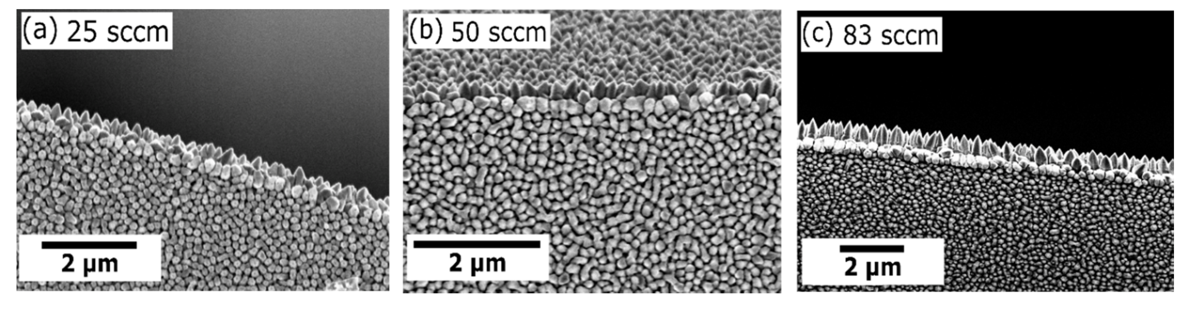
3.3. Oxygen and Argon Flow

By varying the oxygen flow (25, 50, 83 sccm), the surface facets and the nanowhisker tips can be tuned (Figure 4). Zinc oxide has to be deposited from the vapor phase on the substrate to grow as nanowhiskers. The degree of supersaturation of zinc in the vapor phase depends on the oxygen concentration and thus, on the oxygen flow. With increasing flow, sufficient oxygen for the growth of ZnO nanowhiskers is available in the system. The tips and surface facets of the nanowhiskers become sharpened with increasing oxygen flow. The tip angles decreased from 90.0 ± 13.5° (25 sccm O2 flow) to 72.5 ± 7.7° and 65.8 ± 12.4° by increasing the oxygen flow to 50 sccm and 83 sccm, respectively. The relation between the oxygen flow and the nanowhisker morphology reported here is in good agreement with a previous study in which a mixture of ZnO powder and graphite as solid precursors in combination with low oxygen flows (0.25–0.55 sccm) has been used [42].
We also studied the influence of the argon flow, but the changes in the morphology are not as significant as for the variation of the oxygen flow. The corresponding SEM images are shown in the supplementary information (Figure S1).
As already mentioned above in the section about the temperature dependence, an increased nitrogen/oxygen flow can reduce the growth temperatures [23,27]. The carrier gas flow in our experimental setup has much less impact on the nanowhisker morphology than reported elsewhere. The observed lower impact of the argon flow is probably caused by our experimentally limited lower flow of 25–100 sccm in comparison to a previous report by another group (250–500 sccm and 70–200 sccm) [23].

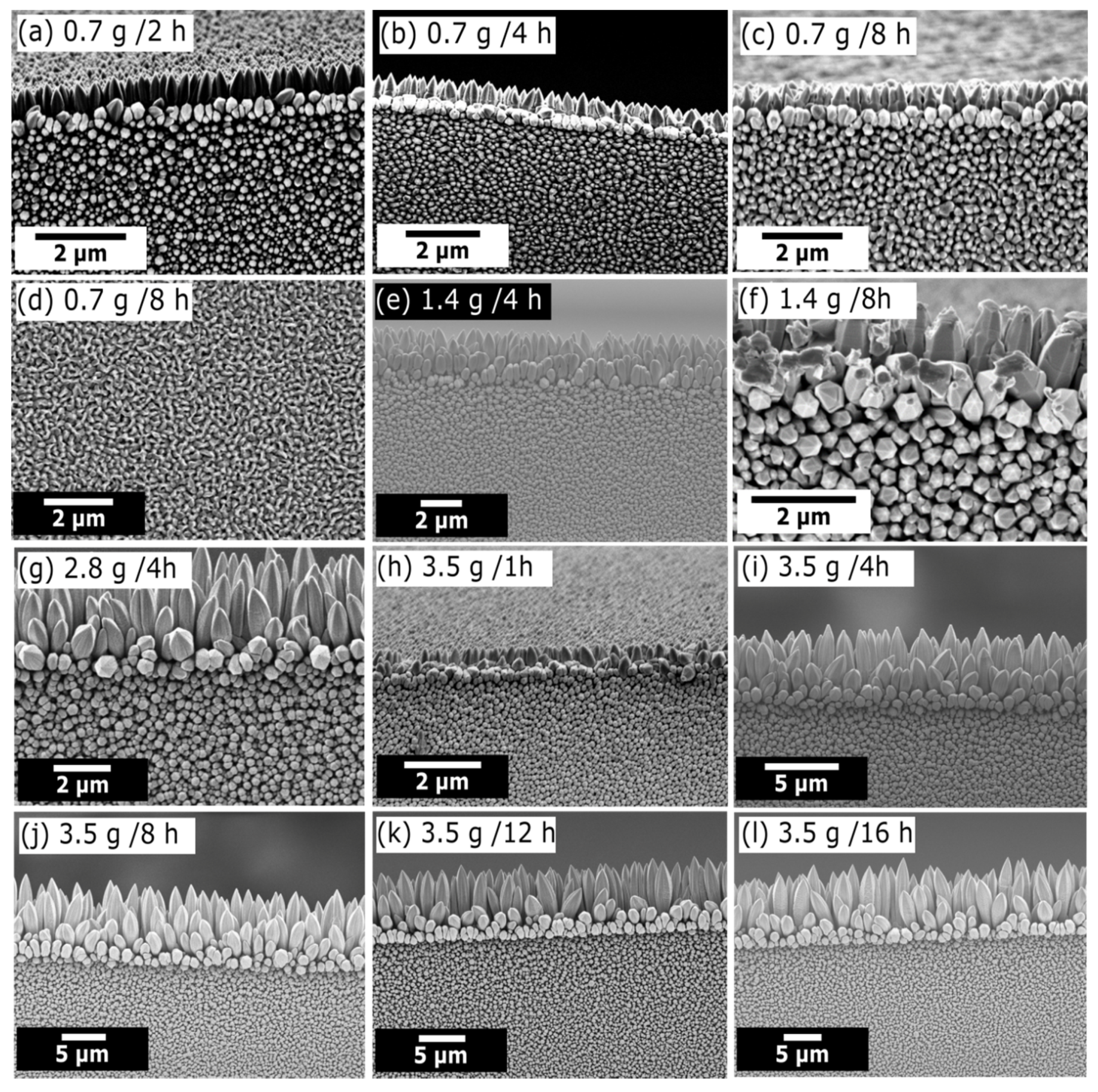
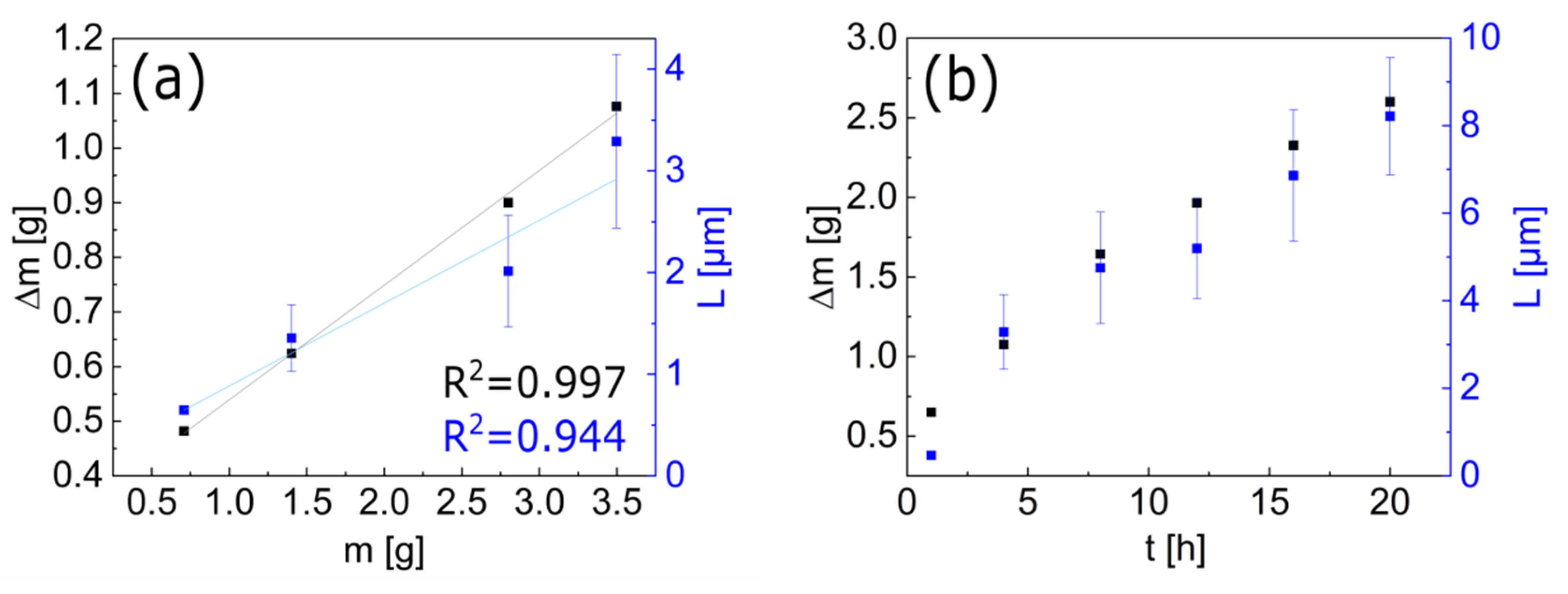
3.4. Precursor Amount and Growth Time
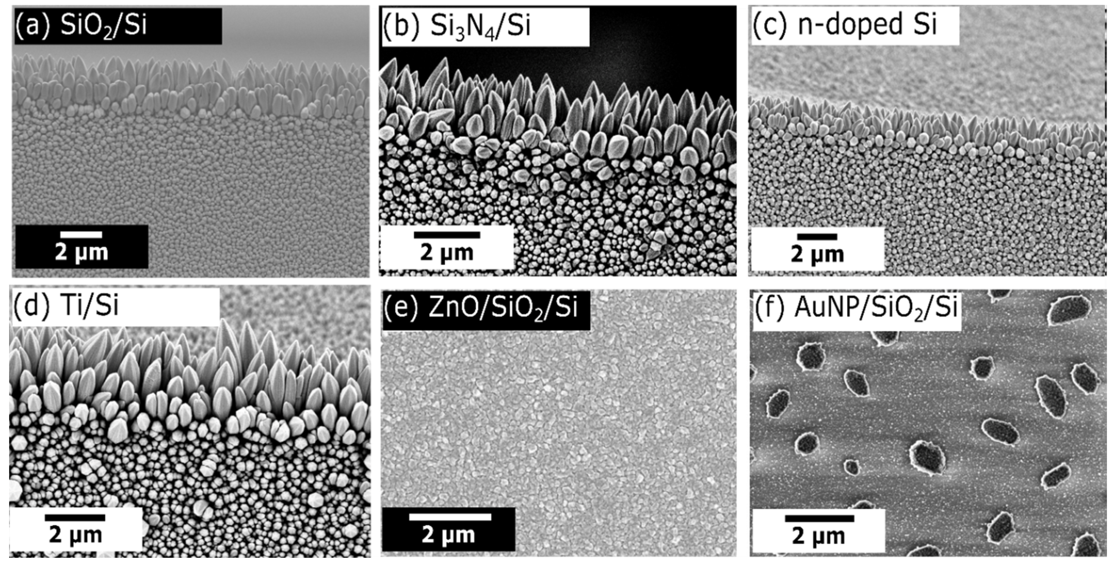
The nanowhisker’s length and diameter can be altered by controlling the amount of the precursor used within the process as well as by adjusting the growth time. On the one hand, changing the growth time (2, 4, 8 h) while using the same amount of zinc precursor (0.7 g) has only a small effect on the morphology of the nanostructures (Figure 5a,b,c). The length and the diameter seem to slightly increase with time but remain within the standard deviation. The lengths are 600 ± 55 nm, 646 ± 41 nm, 697 ± 79 nm and the corresponding diameters were determined to 180 ± 40 nm, 227 ± 55 nm, and 231 ± 48 nm for 2, 4, and 8 h growth time, respectively. Moreover, we found that an increase of the growth time at constant precursor amount (0.7 g) causes the formation of slightly longer nanowhiskers at the edges, but also leads to the growth of a polycrystalline film in the center of the substrate (compare Figure 5c to Figure 5d). On the other hand, doubling the precursor amount (1.4 g) by keeping the growth time constant at 4 h leads to an increase of the nanowhisker’s length to 1.355 ± 0.329 µm (Figure 5e). Another raise of the zinc precursor amount to 2.8 g and 3.5 g results in even longer nanowhiskers (Figure 5g,i). A linear increasing trend of length as a function of precursor amount can be derived as displayed in Figure 6a.
When the precursor amount and the growth time are simultaneously doubled (8 h growth at 1.4 g zinc acetylacetonate hydrate powder), the diameter and the length of the nanowhiskers have a double-fold increase, resulting in 461 ± 171 nm and 1.27 ± 0.11 µm, respectively (Figure 5f). Repeating the study of nanowhisker length vs. growth time with an increased precursor amount (3.5 g) reveals a stronger non-linear increase of the nanowhisker length compared to the former study at a reduced precursor load of 0.7 g (Figure 6b). However, the nanowhiskers morphology and shape remains constant as a function of growth time (Figure 5i–l). The surface facets are clearly visible for all growth times. Note, we could not observe polycrystalline thin film deposition in the center of the sample for all growth times explored herein with the maximum possible precursor load of 3.5 g. To conclude, by using more zinc precursor for the growth process, the absolute value of the precursor amount that vaporizes in the first heating zone and reacts in the third zone is increased. As a consequence, more zinc in quantity is present in the third heating zone which results in an enhancement of the nanowhisker growth in length. The change in the nanowhiskers dimensions occurs even more clearly if the growth time is also increased (Figure 6b). The longest nanowhiskers achieved in our setup within a 20 h growth and an initial precursor amount of 3.5 g reached a length of 8.216 ± 1.34 µm and a diameter of 721 ± 81 nm leading to an aspect ratio of 11.4 (Figure S2).
In detail, we found that precursor consumption is proportional to the initial amount of zinc precursor powder placed in the ceramic crucible (Figure 6a). A high starting precursor amount increases the supersaturation of the vapor phase with the zinc precursor compared to lower precursor amounts and thus, accelerates the growth of the whiskers, which in turn results in faster precursor consumption. To keep the vapor partial pressure constant, more precursor has to evaporate in the first zone. The growth time of course also affects the length of the nanowhiskers, but the proportionality factor is determined by the used amount of zinc precursor, specifically by the vapor partial pressure. The precursor consumption has a non-linear relation to the growth time (Figure 6b) indicating that the growth is faster in the beginning and slows down during the process. This observation explains the deviation of the linearity for whiskers length as a function of time. Note, Baxter et al. reported that an increase in growth time can result in the formation of secondary nanowires, which we cannot confirm in our study [22]. We believe that the increased amount of zinc precursor, compared to their work, keeps the supersaturation of the precursor vapor high enough to allow only the growth of the primary nanowhiskers and suppress secondary nanowire growth [22,46]. However, the morphology turned into a film-like structure when the growth time was increased without adapting the precursor amount. We believe that the axial growth starts to dominate the overall nanowhisker growth at long growth times and reduced precursor partial pressure. As a consequence, the initially free-standing whiskers coalesce forming a nanostructured thin film where the former tips are still apparent at the top surface.

3.5. Substrate Type

With respect to the aforementioned applications, nanowhisker growth has to be achieved on very different substrates. As shown in the previous sections, equally distributed nanowhiskers with clearly observable surface facets and tips grow on SiO2/Si substrates (Figure 7a) by using 1.4 g zinc precursor powder, 580 °C growth temperature, and 4 h growth time. Similar results can be observed on Si3N4 (Figure 7b) and n-doped Si substrates (Figure 7c). The shapes of the surface facets and tips are similar compared to the whiskers on SiO2, while the length and diameter changed to 1.385 ± 0.072 µm and 236 ± 59 nm for Si3N4 and 863 ± 191 nm and 347 ± 77 nm for n-doped Si. Nanowhiskers are also formed on a 40 nm titanium thin film grown by physical vapor deposition on a standard silicon wafer (Figure 7d). The whisker’s length is 1.08 ± 0.37 µm while the diameter is 389 ± 86 nm. However, the tips of these whiskers were more rounded and the surface facets were not as clearly pronounced as on SiO2, Si3N4, and n-doped Si. When running the same process on a pre-defined ZnO buffer layer (deposited by atomic layer deposition), only a polycrystalline film (Figure 7e) without nanowhisker growth was observed. The growth of ZnO nanowires on a ZnO seed layer has been previously reported in the literature [38,47]. However, different precursor combinations have been evaluated in these studies using zinc oxide powder or zinc powder and oxygen for the nanowire growth on a seed layer. Utilizing zinc acetylacetonate hydrate powder and oxygen as precursors as used herein has not been reported for growth on ZnO buffer layers yet, but it might be possible at modified process parameters extending the studied parameter range herein. Lastly, only the growth of ZnO crystallites is obvious in gold nanoparticles (average Au particle diameter 67 ± 25 nm) prepared by dewetting a thin gold film (Figure 7f).
Since the different substrate types have different surface energies, adatom diffusion rates, lattice constants and types and densities of nucleation sites, the morphology of the ZnO nanostructures depends on the used substrate [22]. Therefore, tailoring the morphology from a polycrystalline film or crystallites to nanowhiskers is possible by only changing the substrate while using the same growth parameters. The optimized parameters in this study cause the growth of nanowhiskers with homogeneous dimensions and tip morphology on a SiO2, Si3N4 or n-doped Si substrate.

3.6. Summary of Optimized Growth Parameters

Nanowhiskers can be grown in optimized conditions with aspect ratios from 7.7 to 16.0 depending on the substrate type. It was previously reported in the literature that nanowhiskers with aspect ratios of 4.4 [23], 50.0 [22], and 67.0 [21] have been fabricated by using zinc acetylacetonate and oxygen as precursors. As already discussed above, different experimental setups, as well as substrate types and higher gas flows, might have caused different growth behavior and nanowhiskers with increased dimensions and aspect ratios were fabricated, compared to the structures produced in this work.
The following parameters have been used for the growth of all ZnO nanowhisker samples examined with respect to their field emission properties. A growth temperature of 580 °C, a zinc precursor amount of 3.5 g, and a growth time of 20 h with oxygen and argon flow of 83 sccm and 100 sccm, respectively. The selected growth temperature and gas flow caused the growth of densely packed ZnO nanowhiskers with clearly pronounced surface facets and tips, as described in the growth parameter study. Further, the precursor amount and growth time relation was chosen to attain the largest aspect ratio possible in the tube furnace, which was mostly limited by the size of the precursor boat.
For a sufficient electrical contact to the entire ZnO nanowhisker array needed for the field emission (FE) measurements, the following conductive substrate types have been used: n-doped Si, Ti film on bulk Si, and Ti on a 1.5 µm thick silicon nitride (SiN) membrane. The length and diameter for ZnO nanowhiskers grown on n-doped Si were determined to be 4871 ± 809 nm and 344 ± 115 nm, respectively. For the growth on Ti film, a nanowhisker length of 4392 ± 596 nm and a diameter of 406 ± 255 nm were found, whereas, a length of 2937 ± 493 nm and diameter of 381 ± 224 nm were extracted for nanopillars grown on a Ti-coated SiN membrane. These dimensions have been attained from the nanowhiskers’ cross-section at the center of each sample to get an impression of the geometry of the emitter array at the FE area (Figure 8). These nanowhisker devices are promising candidates for subsequent electron field emission measurements due to their sharp tips and their aspect ratio of about 10 leading to a local electrical field enhancement.

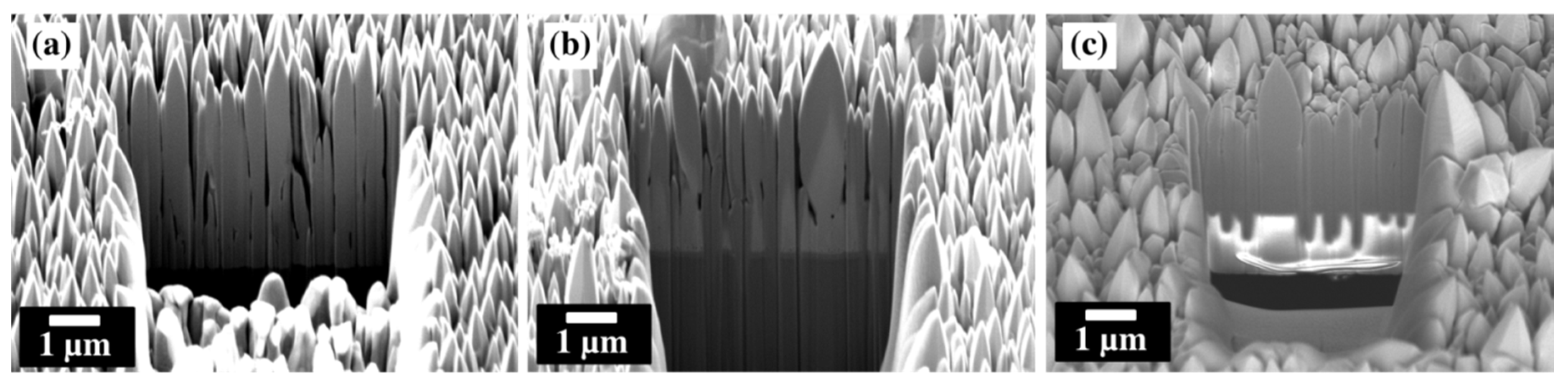
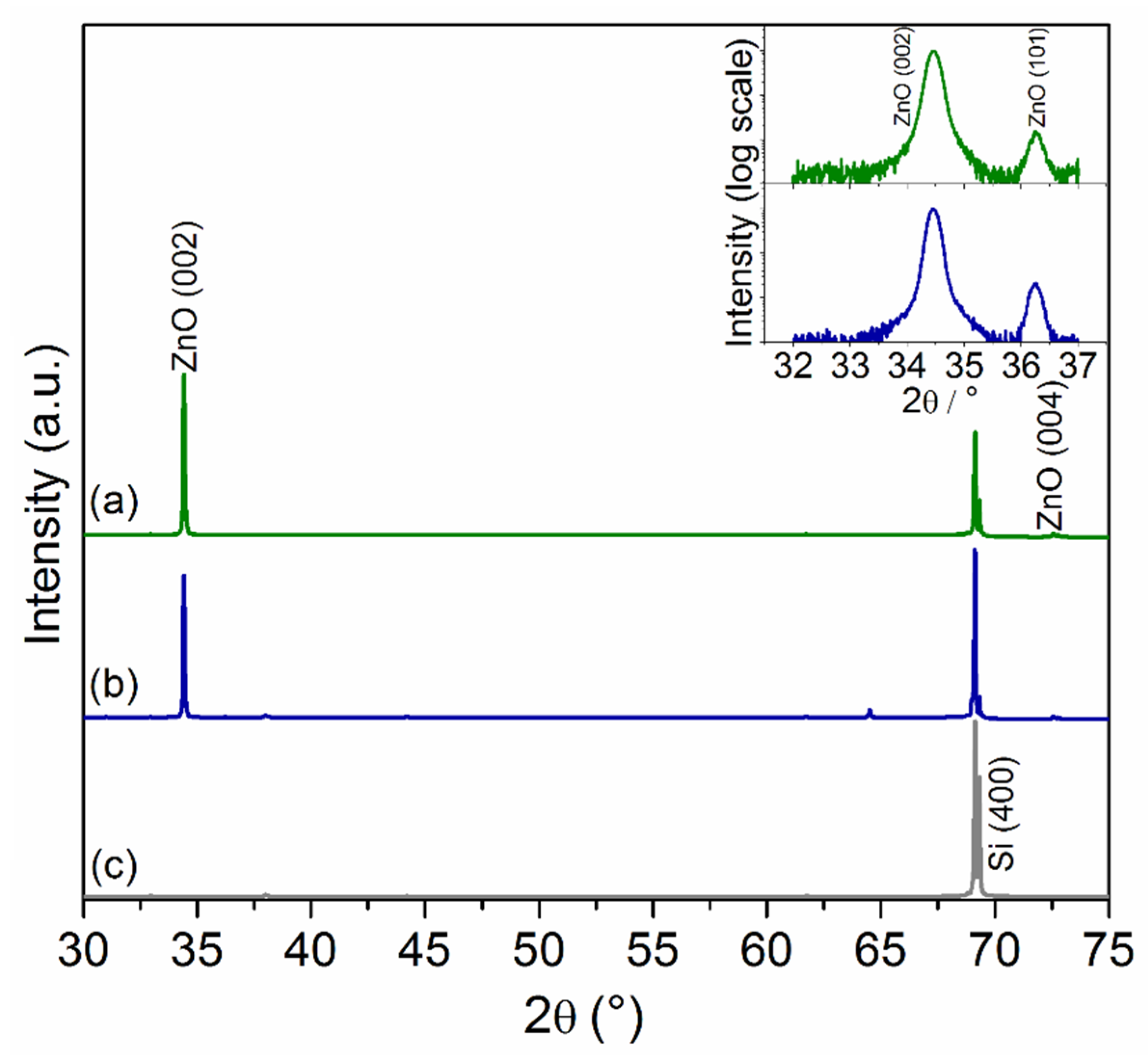
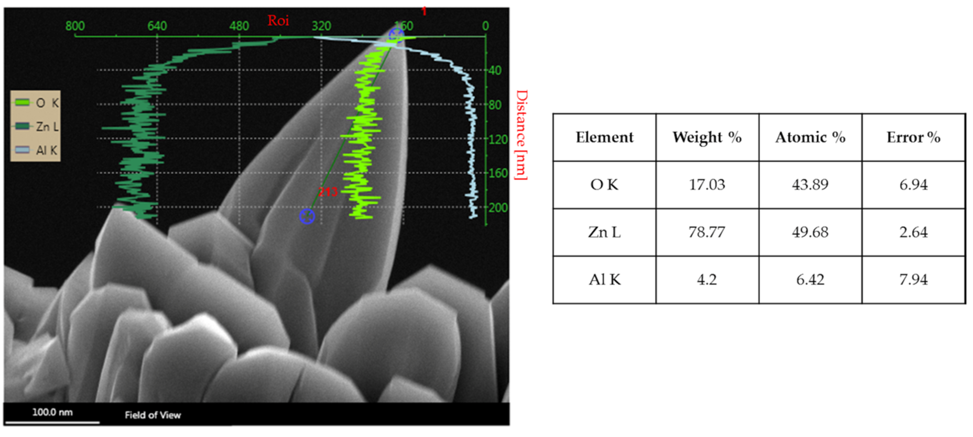
3.7. Structural and Compositional Analysis of Optimized ZnO Nanowhiskers

The XRD spectra (Figure 9) of the optimized nanowhiskers showed diffraction peaks corresponding to the planes (002) and (004) of the hexagonal structure of ZnO (PDF 01-070-2551). The analysis shows a clear preferential alignment of the nanowhiskers into the c-axis direction for both runs. The presence of the low-intensity (101) peak, only possible to be visualized in a log scale (inset of Figure 9), in addition to the (002) and (004) peaks, indicates the occurrence of non-epitaxial growth. XRD scans of two different syntheses run under identical conditions prove the high reproducibility of our synthesis routine.
Energy-dispersive X-ray spectroscopy (Figure 10) of a nanowhisker at the substrate edge revealed a homogenous ratio of zinc and oxygen along the nanowhisker axis. The atomic ratio amounts to 1:1 for Zn:O within the given error.

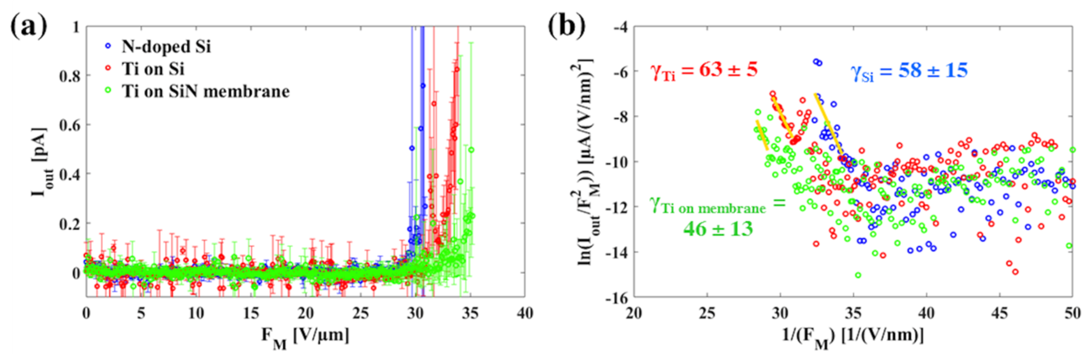
4. Field Emission Measurements

Characteristic field emission—the non-linear increase of emission current—is observed for n-doped Si, Ti film on Si, and a Ti-coated 1.5 µm-thick freestanding SiN membrane upon increasing the applied electrical field (Figure 11a). In detail, the turn-on field—here defined as the applied electric field necessary for the emission current to overcome a 5σ threshold from the data mean—is found to be lower for ZnO nanowhiskers grown on n-doped Si than for nanowhiskers grown on Ti films. Note, the local electric field at the tip of an emitter can be in orders of magnitudes higher than the externally applied electric field, because of the geometrical field enhancement effect, which strongly depends on the emitters’ shape. Linearization of the experimental data according to the Fowler-Nordheim (FN) theory for electron field emission permits the extraction of physical properties of the emitter [45]. By taking a work function of 5.3 eV for ZnO into account [46], the field enhancement factors—describing the ratio between the macroscopic applied electric field and the actual electric field at the surface of the emitter—have been derived for the ZnO nanowhiskers grown on different substrate types (Figure 11b). The field enhancement factor γ for ZnO nanowhiskers grown on n-doped Si and Ti film on bulk Si vary within their standard deviations, which were calculated from the linear fits. However, γ for ZnO nanowhiskers grown on a Ti-coated silicon nitride membrane is lower and will be considered as a separate case in further discussion.
Theoretical calculations based on FN-theory showed that a macroscopic electric field of more than 1700 V/µm would be necessary to permit FE from a flat ZnO film (Figure S2a), which is far above the electrical breakdown strength of a real FE measurement setup. Nevertheless, a field enhancement factor of γ = 58, as derived from the measurements of ZnO nanowhiskers on n-doped Si, enables the emission of electrons at a reasonable applied electric field of less than 35 V/µm (Figure S2b) [48,49].
Several models have been established for the theoretical derivation of the field enhancement factor from the emitter’s geometry [50,51]. The so-called “hemi-ellipsoid on a plane” model can be used to calculate γ for a protrusion having an apex width which is much smaller than the radius of the emitters’ base, as it can be observed for the investigated ZnO nanowhiskers (Figure 8). Specifically, based on determined values of the nanowhisker’s geometry by SEM analysis, theoretical field enhancement factors between 180 and 400 can be calculated for ZnO nanowhiskers grown on bulk substrates being a factor three to eight-fold larger than the extracted γ values from the data fit. However, most models only consider single, free-standing emitters and do not take into account the suppression of the field enhancement effect by electrical field screening arising from neighboring emitters [52,53]. Such a screening effect is rather likely in our case because the distance between neighboring nanowhiskers is rather small (high density) leading to a significant field screening and thus, may explain the deviation of the calculated γ and the field enhancement values, which were derived from the linearized experimental data. As a consequence, one can assume that a less densely packed array of the same ZnO nanowhiskers might have a lower threshold field [54].
The observed small difference in threshold field by about 3 V/µm between ZnO-nanowhiskers on n-doped Si and Ti substrate is in agreement with the field enhancement factors derived from the experimental field emission data by applying the FN model. The aspect ratio of 14 ± 5 for ZnO nanowhiskers grown on n-doped Si is similar to whiskers on Ti with a length-to-diameter ratio of 11 ± 7. Further, the average angle distribution of the nanowhisker tips grown on Ti is only slightly broader with 37 ± 6° than on n-doped Si with 32 ± 4° pointing to an only slightly larger radius of curvature at the emitters’ tip on Ti substrate. Based on the theoretical models, both the aspect ratio as well as the tip curvature should result in a similar enhancement effect. Note, the field emission model by Fowler and Nordheim considers only metal emitters; for semiconducting materials, effects such as electric field penetration, band bending or Schottky barriers at the substrate-electrode interface can alter the electron emission properties and thus, can influence the turn-on field [48].
In literature, turn-on fields for FE from ZnO nanopillars grown without any catalyst vary from about 22.8 V/µm [31] down to 5.3 V/µm [35], depending on the growth setup and substrate type used, but have in common that Zn powder was utilized as precursor [36,37]. The turn-on field is reported to be below 10 V/µm for nanowhiskers grown by vapor-liquid-solid dominated processes because the usage of a catalyst can cause a higher aspect ratio [55] and additionally, offers control about the nanowhisker density, which is essential to reduce the field screening effect [33]. However, the influence of the metal catalyst at the emitters’ tip is often not considered in the analysis of the field emission data.
Finally, ZnO nanowhiskers grown on a Ti-coated, freestanding SiN membrane showed FE at higher turn-on fields than nanowhiskers on bulk substrates. It was expected from earlier reports that the displacement of the membrane under the applied electrostatic field could cause an additional enhancement of the FE [56], however, the contrary effect was observed. On the one hand, the large membrane thickness of 1.5 µm might hinder the bending of the membrane and therefore, suppress any additional enhancement effect. On the other hand, the reduced nanowhisker length on the free-standing silicon nitride membrane might be related to slightly different local temperatures during deposition caused by the low thermal contact between membrane and ceramic boat. As a consequence, a smaller aspect ratio of the nanopillars (8 ± 5) compared to ZnO nanowhiskers grown on bulk substrates is observed. This reduced aspect ratio leads to a smaller field enhancement factor—mirrored in the fitted values (Figure 11b)—which in turn leads to a larger threshold field for electron emission.

5. Conclusions

The effect of the process parameters, such as growth temperature, substrate position and size, gas flow, used amount of zinc precursor, growth time and substrate type on the morphology of ZnO nanowhiskers grown by low-temperature vapor-solid mechanism utilizing zinc acetylacetonate hydrate as a zinc precursor was investigated. The parameters were optimized to receive nanowhiskers with the nearest distribution in dimensions and aspect ratios as high as possible for using them for electron field emission applications.
We showed for the first time, FE measurements from ZnO nanowhiskers grown with the precursors zinc acetylacetonate hydrate and oxygen. Modifications of the turn-on field for FE were observed in dependence on the utilized substrate type (bulk vs. membrane), which were explained by the structural differences of the nanowhiskers, affecting the geometrical field enhancement effect.
Expansion of the accessible experimental parameter range during growth or an additional post-growth treatment, such as thermal annealing or coating by atomic layer deposition, to name a few of them, may give the experimentalist the opportunity to tune the electronic properties of the emitter surface, which could enhance field emission at lower electric fields [57,58,59].
Moreover, nanowhisker growth on thin membranes could potentially be applied in the recently developed nanomembrane detector for MALDI-TOF mass spectrometry, which is a field emission based detection system that has the capability of extending the accessible mass range for a time-of-flight mass spectrometer [56].

Supplementary Materials

The following are available online at https://www.mdpi.com/2079-6412/9/11/698/s1, Table~S1: Overview of the process conditions and the nanowire dimensions including the number of nanowires analyzed. Figure S1: Scanning electron microscope images showing the morphology of ZnO nanowires grown at different argon flows. The used argon flow was (a) 25 sccm. (b) 50 sccm and (c) 100 sccm and (d) 138 sccm. Nanowires grew at all samples and the morphologies of the wires and their surface facets and tips are similar. Figure S2: SEM picture of ZnO nanowires produced by using a Zn precursor amount of 3.5 g and a growth temperature of 20 h. Figure S3: Field emission current over applied electric field for (a) perfectly flat ZnO film and (b) ZnO nanowires. The applied electric field that is necessary to cause electron emission via field emission can tremendously be lowered by the geometrical field enhancement effect [45].

Author Contributions

Conceptualization, C.H., S.H., R.H.B., and R.Z.; Methodology, C.H., S.H., and R.Z.; validation, C.H., S.H., R.H.B., and R.Z.; formal analysis, C.H., and S.H.; investigation, C.H., S.H, L.P. and K.P.F.; resources, R.H.B., and R.Z.; data curation, C.H., S.H., L.P. and K.P.F.; writing—original draft preparation, C.H., and S.H.; writing—review and editing, all authors.; visualization, C.H., and S.H.; supervision, R.H.B., and R.Z.; project administration, R.H.B., and R.Z.

Funding

This research received no external funding.

Acknowledgments

We thank Gerold Schneider (Institute of Advanced Ceramics, Hamburg University of Technology—TUHH, Denickestraße 15, 21073 Hamburg, Germany) for providing the instrumention for X-ray diffraction analysis free of charge.

Conflicts of Interest

The authors declare no conflict of interest.

References

  1. Djurišić, A.B.; Leung, Y.H. Optical Properties of ZnO Nanostructures. Small 2006, 2, 944–961. [Google Scholar] [CrossRef] [PubMed]
  2. Park, W.I. Controlled synthesis and properties of ZnO nanostructures grown by metalorganic chemical vapor deposition: A review. Met. Mater. Int. 2008, 14, 659–665. [Google Scholar] [CrossRef]
  3. Kołodziejczak-Radzimska, A.; Jesionowski, T. Zinc Oxide—From Synthesis to Application: A Review. Materials 2014, 7, 2833–2881. [Google Scholar] [CrossRef] [PubMed]
  4. Ding, M.; Guo, Z.; Zhou, L.; Fang, X.; Zhang, L.; Zeng, L.; Xie, L.; Zhao, H. One-Dimensional Zinc Oxide Nanomaterials for Application in High-Performance Advanced Optoelectronic Devices. Crystals 2018, 8, 223. [Google Scholar] [CrossRef]
  5. Hsu, C.-L.; Chang, S.-J.; Hung, H.-C.; Lin, Y.-R.; Huang, C.-J.; Tseng, Y.-K.; Chen, I.-C. Well-Aligned, Vertically Al-Doped ZnO Nanowires Synthesized on ZnO:Ga/Glass Templates. J. Electrochem. Soc. 2005, 152, G378–G381. [Google Scholar] [CrossRef]
  6. Tynell, T.; Karppinen, M. Atomic layer deposition of ZnO: A review. Semicond. Sci. Technol. 2014, 29, 043001. [Google Scholar] [CrossRef]
  7. Özgür, Ü.; Alivov, Y.I.; Liu, C.; Teke, A.; Reshchikov, M.A.; Doğan, S.; Avrutin, V.; Cho, S.-J.; Morkoç, H. A comprehensive review of ZnO materials and devices. J. Appl. Phys. 2005, 98, 041301. [Google Scholar] [CrossRef] [Green Version]
  8. Gomez, J.L.; Tigli, O. Zinc oxide nanostructures: From growth to application. J. Mater. Sci. 2013, 48, 612–624. [Google Scholar] [CrossRef]
  9. Nasr, B.; Dasgupta, S.; Wang, D.; Mechau, N.; Kruk, R.; Hahn, H. Electrical resistivity of nanocrystalline Al-doped zinc oxide films as a function of Al content and the degree of its segregation at the grain boundaries. J. Appl. Phys. 2010, 108, 103721. [Google Scholar] [CrossRef]
  10. Park, W.I.; Yi, G.-C.; Kim, M.; Pennycook, S.J. ZnO Nanoneedles Grown Vertically on Si Substrates by Non-Catalytic Vapor-Phase Epitaxy. Adv. Mater. 2002, 14, 1841–1843. [Google Scholar] [CrossRef]
  11. Djurišić, A.B.; Ng, A.M.C.; Chen, X.Y. ZnO nanostructures for optoelectronics: Material properties and device applications. Prog. Quantum Electron. 2010, 34, 191–259. [Google Scholar] [CrossRef]
  12. Carretero-Genevrier, A.; Mestres, N.; National, S. Encyclopedia of Nanotechnology; Bhushan, B., Ed.; Springer: Dordrecht, The Netherlands, 2016; ISBN 978-94-017-9779-5. [Google Scholar]
  13. Sui, M.; Gong, P.; Gu, X. Review on one-dimensional ZnO nanostructures for electron field emitters. Front. Optoelectron. 2013, 6, 386–412. [Google Scholar] [CrossRef]
  14. Rivero, P.; Garcia, J.; Quintana, I.; Rodriguez, R. Design of Nanostructured Functional Coatings by Using Wet-Chemistry Methods. Coatings 2018, 8, 76. [Google Scholar] [CrossRef]
  15. Tao, Y.; Pescarmona, P. Nanostructured Oxides Synthesised via scCO2-Assisted Sol-Gel Methods and Their Application in Catalysis. Catalysts 2018, 8, 212. [Google Scholar] [CrossRef]
  16. Greene, L.E.; Law, M.; Goldberger, J.; Kim, F.; Johnson, J.C.; Zhang, Y.; Saykally, R.J.; Yang, P. Low-Temperature Wafer-Scale Production of ZnO Nanowire Arrays. Angew. Chem. Int. Ed. 2003, 42, 3031–3034. [Google Scholar] [CrossRef] [PubMed]
  17. Ko, S.H.; Lee, D.; Hotz, N.; Yeo, J.; Hong, S.; Nam, K.H.; Grigoropoulos, C.P. Digital Selective Growth of ZnO Nanowire Arrays from Inkjet-Printed Nanoparticle Seeds on a Flexible Substrate. Langmuir 2012, 28, 4787–4792. [Google Scholar] [CrossRef]
  18. Ko, S.H.; Lee, D.; Kang, H.W.; Nam, K.H.; Yeo, J.Y.; Hong, S.J.; Grigoropoulos, C.P.; Sung, H.J. Nanoforest of Hydrothermally Grown Hierarchical ZnO Nanowires for a High Efficiency Dye-Sensitized Solar Cell. Nano Lett. 2011, 11, 666–671. [Google Scholar] [CrossRef]
  19. Wan, H.; Ruda, H.E. A study of the growth mechanism of CVD-grown ZnO nanowires. J. Mater. Sci. Mater. Electron. 2010, 21, 1014–1019. [Google Scholar] [CrossRef]
  20. Hamzah, N.A.B.; Pung, S.Y.; Sreekantan, S.; Aziz, S.N.Q.A.B.A. Synthesis and Growth Mechanism of Catalyst-Free ZnO Nanowires Using Chemical Vapour Deposition. Adv. Mater. Res. 2012, 620, 320–324. [Google Scholar] [CrossRef]
  21. Satoh, M.; Tanaka, N.; Ueda, Y.; Ohshio, S.; Saitoh, H. Epitaxial Growth of Zinc Oxide Whiskers by Chemical-Vapor Deposition under Atmospheric Pressure. Jpn. J. Appl. Phys. 1999, 38, L586–L589. [Google Scholar] [CrossRef]
  22. Baxter, J.B.; Aydil, E.S. Metallorganic Chemical Vapor Deposition of ZnO Nanowires from Zinc Acetylacetonate and Oxygen. J. Electrochem. Soc. 2009, 156, H52–H58. [Google Scholar] [CrossRef]
  23. Liu, S.-C.; Wu, J.-J. Low-temperature and catalyst-free synthesis of well-aligned ZnO nanorods on Si (100). J. Mater. Chem. 2002, 12, 3125–3129. [Google Scholar] [CrossRef]
  24. Wagner, R.S.; Ellis, W.C. Vapor-Liquid-Solid Mechanism of Single Crystal Growth. Appl. Phys. Lett. 1964, 4, 89–90. [Google Scholar] [CrossRef]
  25. Wu, Y.; Yang, P. Direct Observation of Vapor−Liquid−Solid Nanowire Growth. J. Am. Chem. Soc. 2001, 123, 3165–3166. [Google Scholar] [CrossRef]
  26. Huang, M.H.; Wu, Y.; Feick, H.; Tran, N.; Weber, E.; Yang, P. Catalytic Growth of Zinc Oxide Nanowires by Vapor Transport. Adv. Mater. 2001, 13, 113–116. [Google Scholar] [CrossRef]
  27. Wu, J.-J.; Liu, S.-C. Low-Temperature Growth of Well-Aligned ZnO Nanorods by Chemical Vapor Deposition. Adv. Mater. 2002, 14, 215–218. [Google Scholar] [CrossRef]
  28. Wu, J.-J.; Liu, S.-C. Catalyst-Free Growth and Characterization of ZnO Nanorods. J. Phys. Chem. B 2002, 106, 9546–9551. [Google Scholar] [CrossRef]
  29. Garry, S.; McCarthy, É.; Mosnier, J.-P.; McGlynn, E. Influence of ZnO nanowire array morphology on field emission characteristics. Nanotechnology 2014, 25, 135604. [Google Scholar] [CrossRef] [Green Version]
  30. Fang, Y.; Wong, K.M.; Lei, Y. Synthesis and field emission properties of different ZnO nanostructure arrays. Nanoscale Res. Lett. 2012, 7, 197. [Google Scholar] [CrossRef]
  31. Kuo, S.-Y.; Lin, H.-I. Field emission characteristics of zinc oxide nanowires synthesized by vapor-solid process. Nanoscale Res. Lett. 2014, 9, 70. [Google Scholar] [CrossRef]
  32. Li, S.Y.; Lin, P.; Lee, C.Y.; Tseng, T.Y. Field emission and photofluorescent characteristics of zinc oxide nanowires synthesized by a metal catalyzed vapor-liquid-solid process. J. Appl. Phys. 2004, 95, 3711–3716. [Google Scholar] [CrossRef] [Green Version]
  33. Wang, X.D.; Zhou, J.; Lao, C.S.; Song, J.H.; Xu, N.S.; Wang, Z.L. In Situ Field Emission of Density-Controlled ZnO Nanowire Arrays. Adv. Mater. 2007, 19, 1627–1631. [Google Scholar] [CrossRef]
  34. Zhu, Y.W.; Zhang, H.Z.; Sun, X.C.; Feng, S.Q.; Xu, J.; Zhao, Q.; Xiang, B.; Wang, R.M.; Yu, D.P. Efficient field emission from ZnO nanoneedle arrays. Appl. Phys. Lett. 2003, 83, 144–146. [Google Scholar] [CrossRef]
  35. Zhang, Z.; Yuan, H.; Zhou, J.; Liu, D.; Luo, S.; Miao, Y.; Gao, Y.; Wang, J.; Liu, L.; Song, L.; et al. Growth Mechanism, Photoluminescence, and Field-Emission Properties of ZnO Nanoneedle Arrays. J. Phys. Chem. B 2006, 110, 8566–8569. [Google Scholar] [CrossRef]
  36. Shen, G.Z.; Bando, Y.; Liu, B.D.; Golberg, D.; Lee, C.-J. Characterization and Field-Emission Properties of Vertically Aligned ZnO Nanonails and Nanopencils Fabricated by a Modified Thermal-Evaporation Process. Adv. Funct. Mater. 2006, 16, 410–416. [Google Scholar] [CrossRef]
  37. Tseng, Y.-K.; Huang, C.-J.; Cheng, H.-M.; Lin, I.-N.; Liu, K.-S.; Chen, I.-C. Characterization and Field-Emission Properties of Needle-like Zinc Oxide Nanowires Grown Vertically on Conductive Zinc Oxide Films. Adv. Funct. Mater. 2003, 13, 811–814. [Google Scholar] [CrossRef]
  38. Li, C.; Fang, G.; Li, J.; Ai, L.; Dong, B.; Zhao, X. Effect of Seed Layer on Structural Properties of ZnO Nanorod Arrays Grown by Vapor-Phase Transport. J. Phys. Chem. C 2008, 112, 990–995. [Google Scholar] [CrossRef]
  39. Schneider, C.A.; Rasband, W.S.; Eliceiri, K.W. NIH Image to ImageJ: 25 years of image analysis. Nat. Methods 2012, 9, 671–675. [Google Scholar] [CrossRef]
  40. Menzel, A.; Goldberg, R.; Burshtein, G.; Lumelsky, V.; Subannajui, K.; Zacharias, M.; Lifshitz, Y. Role of Carrier Gas Flow and Species Diffusion in Nanowire Growth from Thermal CVD. J. Phys. Chem. C 2012, 116, 5524–5530. [Google Scholar] [CrossRef]
  41. Hassan, N.K.; Hashim, M.R.; Mahdi, M.A.; Allam, N.K. A Catalyst-Free Growth of ZnO Nanowires on Si (100) Substrates: Effect of Substrate Position on Morphological, Structural and Optical Properties. ECS J. Solid State Sci. Technol. 2012, 1, P86–P89. [Google Scholar] [CrossRef]
  42. Babu, E.S.; Saravanakumar, B.; Ravi, G.; Yuvakkumar, R.; Ganesh, V.; Guduru, R.K.; Kim, S. Zinc oxide nanotips growth by controlling vapor deposition on substrates. J. Mater. Sci. Mater. Electron. 2018, 29, 6149–6156. [Google Scholar] [CrossRef]
  43. Lupan, O.; Emelchenko, G.A.; Ursaki, V.V.; Chai, G.; Redkin, A.N.; Gruzintsev, A.N.; Tiginyanu, I.M.; Chow, L.; Ono, L.K.; Roldan Cuenya, B.; et al. Synthesis and characterization of ZnO nanowires for nanosensor applications. Mater. Res. Bull. 2010, 45, 1026–1032. [Google Scholar] [CrossRef]
  44. Huber, F.; Puchinger, A.; Ahmad, W.; Madel, M.; Bauer, S.; Thonke, K. Controlled growth of ZnO layers and nanowires using methane as reducing precursor. J. Mater. Res. 2017, 32, 4087–4094. [Google Scholar] [CrossRef]
  45. Mohanta, S.K.; Kim, D.C.; Cho, H.K.; Chua, S.J.; Tripathy, S. Structural and optical properties of ZnO nanorods grown by metal organic chemical vapor deposition. J. Cryst. Growth 2008, 310, 3208–3213. [Google Scholar] [CrossRef]
  46. Menzel, A.; Subannajui, K.; Bakhda, R.; Wang, Y.; Thomann, R.; Zacharias, M. Tuning the Growth Mechanism of ZnO Nanowires by Controlled Carrier and Reaction Gas Modulation in Thermal CVD. J. Phys. Chem. Lett. 2012, 3, 2815–2821. [Google Scholar] [CrossRef]
  47. Cha, S.N.; Song, B.G.; Jang, J.E.; Jung, J.E.; Han, I.T.; Ha, J.H.; Hong, J.P.; Kang, D.J.; Kim, J.M. Controlled growth of vertically aligned ZnO nanowires with different crystal orientation of the ZnO seed layer. Nanotechnology 2008, 19, 235601. [Google Scholar] [CrossRef]
  48. Liang, S.-D. Quantum Tunneling and Field Electron Emission Theories; World Scientific: Singapure, 2014; ISBN 978-981-4440-21-9. [Google Scholar]
  49. Minami, T.; Miyata, T.; Yamamoto, T. Work function of transparent conducting multicomponent oxide thin films prepared by magnetron sputtering. Surf. Coatings Technol. 1998, 108–109, 583–587. [Google Scholar] [CrossRef]
  50. Forbes, R.G.; Edgcombe, C.; Valdrè, U. Some comments on models for field enhancement. Ultramicroscopy 2003, 95, 57–65. [Google Scholar] [CrossRef]
  51. Biswas, D. A universal formula for the field enhancement factor. Phys. Plasmas 2018, 25, 043113. [Google Scholar] [CrossRef]
  52. Jo, S.H.; Lao, J.Y.; Ren, Z.F.; Farrer, R.A.; Baldacchini, T.; Fourkas, J.T. Field-emission studies on thin films of zinc oxide nanowires. Appl. Phys. Lett. 2003, 83, 4821–4823. [Google Scholar] [CrossRef] [Green Version]
  53. Zhao, Q.; Zhang, H.Z.; Zhu, Y.W.; Feng, S.Q.; Sun, X.C.; Xu, J.; Yu, D.P. Morphological effects on the field emission of ZnO nanorod arrays. Appl. Phys. Lett. 2005, 86, 203115. [Google Scholar] [CrossRef]
  54. Ahmad, A.; Tripathi, V.K.; Shang, X.; Wang, M.; Qu, S. Model calculation of the scanned field enhancement factor of CNTs. Nanotechnology 2006, 17, 3798–3801. [Google Scholar] [CrossRef]
  55. Lee, C.J.; Lee, T.J.; Lyu, S.C.; Zhang, Y.; Ruh, H.; Lee, H.J. Field emission from well-aligned zinc oxide nanowires grown at low temperature. Appl. Phys. Lett. 2002, 81, 3648–3650. [Google Scholar] [CrossRef]
  56. Park, J.; Qin, H.; Scalf, M.; Hilger, R.T.; Westphall, M.S.; Smith, L.M.; Blick, R.H. A mechanical nanomembrane detector for time-of-flight mass spectrometry. Nano Lett. 2011, 11, 3681–3684. [Google Scholar] [CrossRef]
  57. Huang, J.-M.; Tsai, S.-Y.; Ku, C.-S.; Lin, C.-M.; Chen, S.-Y.; Lee, H.-Y. Enhanced electrical properties and field emission characteristics of AZO/ZnO-nanowire core–shell structures. Phys. Chem. Chem. Phys. 2016, 18, 15251–15259. [Google Scholar] [CrossRef]
  58. Yang, J.H.; Lee, S.Y.; Song, W.S.; Shin, Y.S.; Park, C.; Kim, H.-J.; Cho, W.; An, K.-S. Field emission properties of ZnO nanorods coated with NiO film. J. Vac. Sci. Technol. B 2008, 26, 1021. [Google Scholar] [CrossRef]
  59. Henkel, C.; Zierold, R.; Kommini, A.; Haugg, S.; Thomason, C.; Aksamija, Z.; Blick, R.H. Resonant Tunneling Induced Enhancement of Electron Field Emission by Ultra-Thin Coatings. Sci. Rep. 2019, 9, 6840. [Google Scholar] [CrossRef]
Figure 1. Schematic (a) of the vapor-solid growth process and (b) of the tube furnace including the connected gas lines, the ceramic boat with the precursor, and the ceramic boat with the substrate.
Coatings 09 00698 g001
Figure 2. Top-view SEM images of the ZnO nanostructures morphology according to the substrate position during the growth process: (a) in the front, (b) in the center and (c) in the back of the ceramic boat. The structures have been grown within the same process at 550 °C, 50 sccm Ar and 25 sccm O2 flow.
Coatings 09 00698 g002
Figure 3. SEM images of ZnO nanostructures formed at different growth temperatures. The morphology of the structures varied from polycrystalline films (a,e) to nanowhiskers (bd) with different characteristics of the surface facets and tips as a function of temperature. The structures are fabricated by using 50 sccm Ar and 25 sccm O2. (f) The consumption of the zinc acetylacetonate hydrate powder showed a linear dependence in the temperature range with a rate of 0.83 ± 0.04 mg/°C.
Coatings 09 00698 g003
Figure 4. SEM images showing the morphology of ZnO nanowhiskers grown at different oxygen flows (a) 25 sccm, (b) 50 sccm, and (c) 83 sccm. Nanowhiskers facets and tips become more pronounced with increasing flow.
Coatings 09 00698 g004
Figure 5. Scanning electron micrographs of the nanowhiskers’ morphology as a function of the amount of zinc precursor and the growth time. By using 0.7 g zinc precursor powder, the nanowhiskers grow for (a) 2 h, (b) 4 h, and (c,d) 8 h. The results of nanowhisker growth for a zinc precursor amount of 1.4 g at growth times for 4 h and 8 h are shown in (e) and (f), respectively. By using 2.8 g zinc precursor and 4 h growth time, the nanowhiskers in (g) are formed. A zinc precursor amount of 3.5 g is used for the samples (h)–(l), while the growth time is varied between (h) 1 h, (i) 4 h, (j) 8 h, (k) 12 h, and (l) 16 h, respectively.
Coatings 09 00698 g005
Figure 6. Correlations between the used and consumed amount of zinc precursor, the growth time, and the nanowhiskers’ lengths. (a) The zinc precursor consumption is proportional to the used amount of precursor at 4 h growth leading to a precursor usage of 0.210 ± 0.007 g/g of employed precursor (black squares). Also, the length of the nanowhiskers is proportional to the used precursor amount within a 4 h growth process with a factor of 0.815 ± 0.114 µm/g (blue squares). (b) The precursor consumption (black squares), as well as the whiskers’ lengths (blue squares), show a non-linear dependence on the growth time when using a precursor amount of 3.5 g.
Coatings 09 00698 g006
Figure 7. SEM pictures of nanowhiskers grown on different substrate types. The material of the substrate was (a) 100 nm SiO2/Si, (b) 100 nm Si3N4/Si, (c) n-doped Si, (d) 40 nm Ti/Si, (e) 30 nm ZnO/100 nm SiO2/ Si and (f) gold nanoparticles (average diameter 67 ± 25 nm) on 100 nm SiO2/Si. Depending on the type of the substrate, nanowhiskers, polycrystalline films or crystallites have formed.
Coatings 09 00698 g007
Figure 8. Cross-sectional SEM micrographs after focused ion beam milling of ZnO nanowhiskers grown on (a) n-doped Si, (b) Ti, and (c) a Ti-coated SiN membrane. The SEM images were taken with a tilting angle of 54°.
Coatings 09 00698 g008
Figure 9. XRD spectra of ZnO nanowhiskers grown in optimized conditions at different runs (a), (b) on silicon wafers (c). Reflections at 2θ ≈ 38° and 64° arise from the equipment sample holder of aluminum. Inset spectra were obtained via GI-XRD (1° incident angle).
Coatings 09 00698 g009
Figure 10. EDX line scan of a ZnO nanowhisker at the substrate edge grown in optimized conditions. The intensity profile reveals a constant ratio of Zn and O in 1:1 stoichiometry along the nanowhiskers axis. The aluminum originates from the sample holder.
Coatings 09 00698 g010
Figure 11. (a) For each sample type, the mean of two subsequent measurements of the output current (Iout) in dependence on the macroscopic electric field (FM) is shown, with the standard deviation as an error bar. Offset and slope—caused by the transimpedance amplifier and the ohmic resistance of the plate-capacitor like measurement assembly, respectively—have already been subtracted from the data. (b) FN theory was used to derive γ from the linearized experimental data [45] and the errors were calculated from the standard deviations of the linear fits.
Coatings 09 00698 g011

