Article

Surface Texture Evolution of Fused Silica in a Combined Process of Atmospheric Pressure Plasma Processing and Bonnet Polishing

1
Centre for Precision Engineering, Harbin Institute of Technology, Harbin 150001, China
2
National Facility for Ultra Precision Surfaces, University of Huddersfield, Saint Asaph LL17 0JD, UK
3
Department of Physics and Astronomy, University College London, London WC1E 6BT, UK
4
Zeeko Ltd, Colville, Leicestershire LE67 3WF, UK
5
Research Center for Space Optical Engineering, Harbin Institute of Technology, Harbin 150001, China
*
Authors to whom correspondence should be addressed.
Coatings 2019, 9(10), 676; https://doi.org/10.3390/coatings9100676
Submission received: 30 August 2019 / Revised: 11 October 2019 / Accepted: 15 October 2019 / Published: 18 October 2019
(This article belongs to the Section Surface Characterization, Deposition and Modification)

Abstract

:
The increasing demand for precision optical components invokes the requirement of advanced fabrication techniques with high efficiency. Atmospheric pressure plasma processing (APPP), based on chemical etching, has a high material removal rate and a Gaussian-shaped influence function, which is suitable to generate complex structures and correct form errors. Because of the pure chemical etching, an optically smooth surface cannot be achieved using only APPP. Thus, bonnet polishing (BP) with a flexible membrane tool, also delivering a Gaussian influence-function, is introduced to smooth the surface after APPP. In this paper, the surface texture evolution in the combined process of APPP and BP is studied. The etched texture with increased removal depth of APPP is presented and analyzed. Subsequently, the processed substrates are smoothed by BP. The texture smoothing and the roughness improvement is investigated in detail. The experimental results show that the APPP etched pits coalesce with each other and transform into irregular convex-concave structures, with roughness degraded to about 25 nm arithmetical mean deviation (Ra). The APPP etched texture can be successfully smoothed to 1.5 nm Ra, with 0.2–1 μm material removal of BP.

1. Introduction

Fused silica has excellent optical properties, mechanical properties and high chemical durability, which make it widely used in advanced optical systems. In particular, there are thousands of aspherical lenses and window mirrors made of fused silica in high-power laser projects, such as the National Ignition Facility [1]. To meet the huge demands for such optics, many state-of-the-art optical fabrication techniques have been developed. ‘Precessions’ polishing technology, originally developed by the Optical Science Laboratory, has been further developed and commercialized by Zeeko Ltd. [2]. The standard polishing tool of the ‘Precessions’ technology is an inflated spherical membrane (the ‘bonnet’) covered with a standard polishing cloth. The compliance of such a tool allows it to conform along a tool path to the varying local topography of aspheric or freeform surfaces, avoiding tool-misfit [3,4,5,6]. The presence of a physical pad in this process is important in “bridging the peaks of micro-roughness”, allowing polishing of ground or rough surfaces, as well correcting form-errors. Magnetorheological finishing (MRF) was invented at the Luikov Institute of Heat and Mass Transfer in Minsk and then developed at the Center for Optics Manufacturing [7]. The polishing tool of MRF is a ribbon of magnetorheological fluid locally stiffened by a magnetic field. This process does not suffer misfit issues on aspheres and freeforms [8], but the absence of a pad renders it unsuitable for pre-polishing a rough surface: it is a finishing process, as the name implies. For ultra-precision finishing, ion beam figuring (IBF) provides nanometer-scale material removal [9,10], but again, without polishing capability. In addition, the shear-thickening polishing (STP) [11,12], elastic emission machine (EEM) [13] and fluid jet polishing (FJP) [14] also draw much research attention.
In the last decades, plasma processing techniques utilizing chemical etching by fluorine radicals were proposed. Based on multiple plasma generation methods, various plasma processing techniques have been developed for different applications. Inductively coupled plasma (ICP) is utilized in reactive atom plasma (RAP) processing [15] and arc-enhanced plasma machining (AEPM) [16] to generates reactive plasma jet, which is available for fast figuring and removing subsurface damage. Capacitively coupled plasma (CCP) is used in chemical vaporization machining (CVM) and atmospheric pressure plasma processing (APPP), which offer various machining modes, such as flat machining with rotatory electrodes [17], slicing machining with wire electrodes [18] and contact machining mode [19]. Based on microwave plasma technology, plasma jet machining (PJM) was developed and applied for fabricating aspherical and free from surfaces [20].
However, plasma processing cannot pre-polish a rough surface, and in fact, tends to degrade the input surface texture due to the nature of chemical etching [21,22]. Consequently, post-polishing methods have been introduced to obtain optical smooth surfaces after the plasma processing step. Subrahmanyan et al. proposed the integrated manufacturing process (IMP) including RAP and post-polishing using flexible laps. Such polishing acts as a low-pass spatial filter to improve the surface roughness down to circa 1 nm [23]. Mori et al. combined elastic emission machining (EEM) and CVM for fabricating coherent X-ray optics, in which roughness in the spatial-wavelength range <1 μm was removed rapidly by EEM [24,25]. Based on the thermal effect of the plasma jet, Arnold et al. developed plasma jet polishing (PJP) to improve surface quality before PJM [26]. Su et al. combined APPP and BP for fabricating freeform surfaces [27,28]. APPP was used to generate surface form firstly, and then BP was used to smooth the surface without damaging the generated form [29]. These studies indicate that post-polishing of some kind is inevitable for plasma processing to be widely used. Furthermore, understanding the surface texture evolution in plasma processing and post-polishing is critical to optimize the end-to-end process.
In this paper, we focus on the surface texture evolution in the combined process of APPP and BP. The fused silica substrates were processed by APPP with increased depth. The formation process of the plasma etched texture was presented and analyzed. Then, the APPP processed substrates were polished layer by layer to investigate the smoothing process. In addition, the roughness change-law in the whole combined process was obtained.

2. Combined Process and Experimental Details

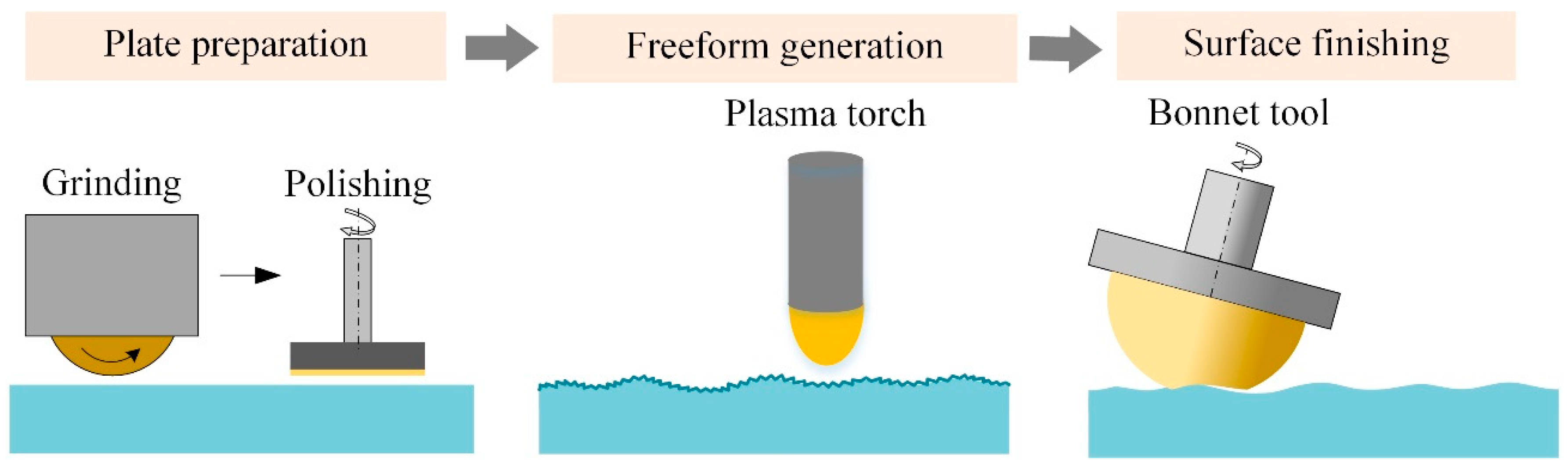
2.1. Combination of APPP and BP

The combination of APPP and BP can be used to generate freeform surfaces [29] and correct form errors on fused silica. Figure 1 shows the schematic diagram of freeform generation. The plate is prepared using conventional grinding and polishing. For conventional optical fabrication techniques, the material removal is realized mainly through mechanical processes, which introduces subsurface damage (SSD) inevitably. It is commonly thought that a high removal rate (exemplified by grinding) and low SSD (exemplified by polishing) are mutually contradictory. Based on chemical etching, APPP can deliver high material removal rates and narrow influence functions to generate freeform surfaces, without introducing SSD, but at the expense of a degraded texture. The texture degradation brings form error measurement difficulty in iterative fabrication process, and also makes the surface quality unacceptable for optical systems. Hence, BP is introduced to post-polish the plasma etched substrates to a measurable quality or final desired texture. This finishing step is conducted at a constant feed rate with the aim of removing a uniform ‘skin’ over the substrate. To understand the combined process, the texture evolution needs to be investigated.

2.2. Preparation of Sample Substrates

The sample substrates were fused silica (JGS2) with a thickness of 3 mm provided by the China Building Materials Academy (Beijing, China). The samples were pre-polished using a conventional pitch lap with CeO2 slurry to about 2 nm Ra. They were then fully cleaned in anhydrous alcohol and deionized water using an ultrasonic cleaner, and dried at room temperature.

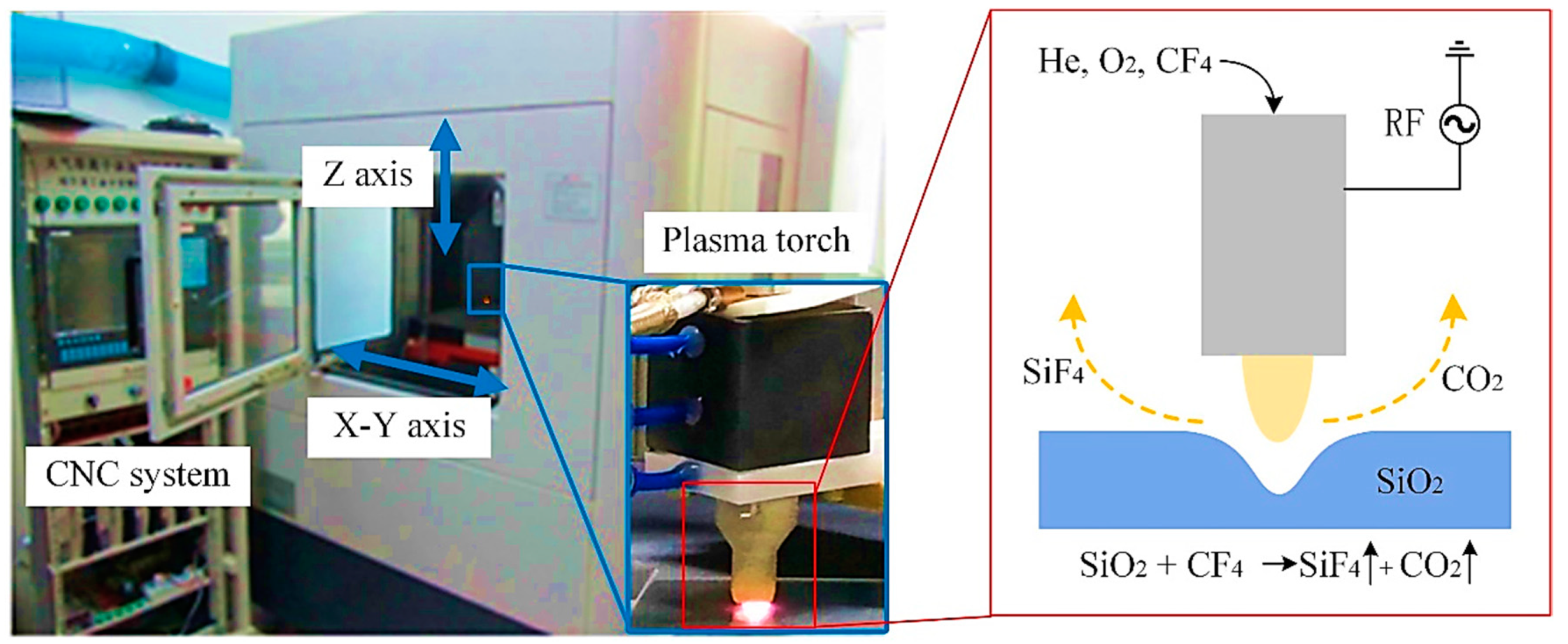
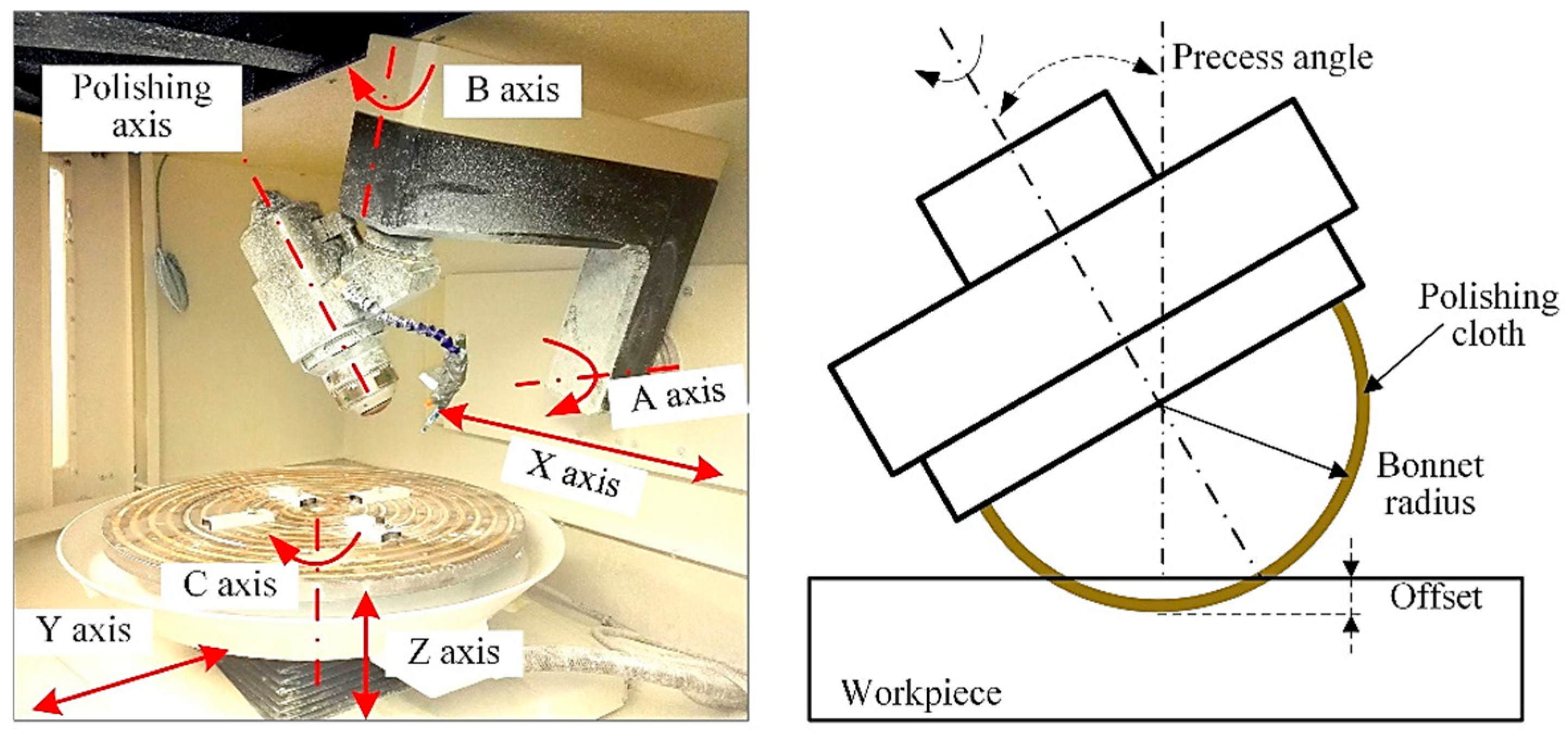
2.3. Experimental Setup

Figure 2 shows the APPP experimental setup and the material removal mechanism. In APPP, working gases, such as He, CF4 and O2, are introduced into the plasma torch. The plasma jet, including reactive fluorine radicals, is generated excited by the radio-frequency (RF) supply. The fluorine radicals react with SiO2 to produce volatile SiF4, removing material. The APPP processing parameters are given in Table 1.
The flexible membrane tools of BP can rapidly achieve ultra-smooth surface texture. A IRP600 7-axis CNC polishing machine (Zeeko Ltd., Leicestershire, UK) was used in this study, shown in Figure 3. Table 2 gives the polishing parameters.
The profilometer (Form Talysurf PGI 1240, Taylor Hobson, Leicester, UK) and interferometer (μPhase 2 HR, Fisba, Gallen, Switzerland) were used to measure removal depth. A white-light interferometer (MicroAXM, ADE Phase Shift, Tucson, AZ, USA) was used to measure the surface texture. The scanning electron microscope (SEM, ZEISS Merlin Compact, Zeiss, Oberkochen, Germany) was used to analyze the chemical composition on substrate in the combined process.

3. Results

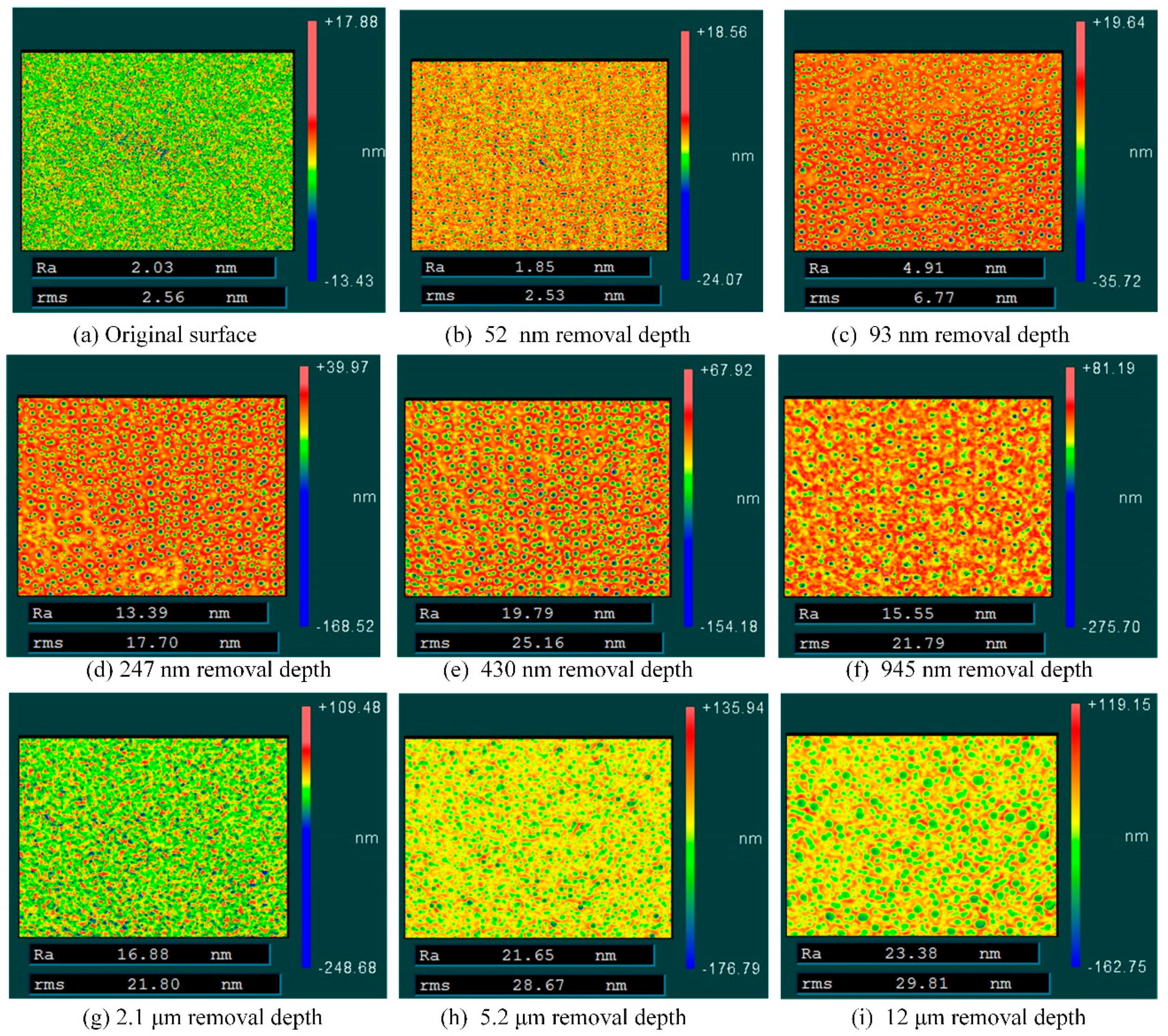
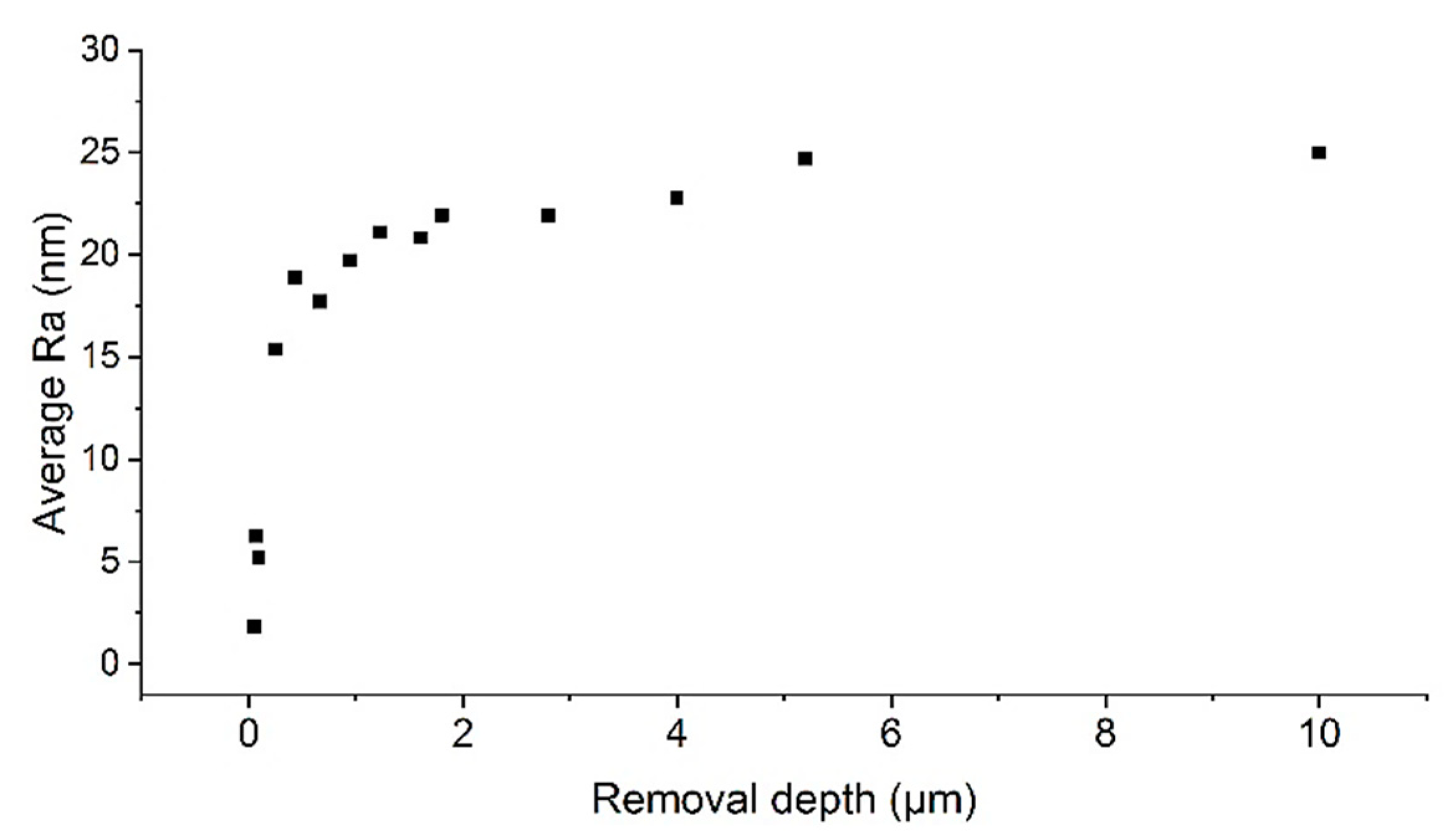
3.1. Surface Texture Evolution after APPP

To investigate the surface texture after APPP, trenches were processed under different feed rates. The trench depth was controlled from tens of nanometers to tens of microns. Figure 4 shows the measurement results for the trenches. The textures at the measurement points in Figure 4 were obtained using the white light interferometer. The measurements were conducted three times for each trench to obtain the average roughness. In this way, the correlation between the surface texture and the removal depth of APPP was obtained.
Figure 5 shows a series of surface texture under different removal depth after APPP. The original surface before APPP exhibited a typical polished texture with 2 nm Ra, as shown in Figure 5a. After 52 nm material removal etched by APPP, the smooth surface was degraded and some etched pits appeared, as shown in Figure 5b. It is known that in polishing the material removal is realized through the mechanical and chemical effect. Even though the load exerted by individual abrasive particles is much smaller than that in grinding, some micro-cracks can remain after polishing [30]. When the plasma jet contacts the substrate surface, the reactive fluorine radicals react with the sidewalls of the micro-cracks. Thus, the micro-cracks open and etched pits form. Compared with that on ground fused silica after APPP [31], these etched pits are much smaller and shallower, with the width of only tens of nanometers. With the material removal increasing from 52 to 945 nm, these etched pits become wider and deeper, as shown in Figure 5b–e. At 945 nm, the etched pits start to intersect gradually and coalesce with each other, shown in Figure 5f. After coalescing of the separated pits, the surface texture transfers to irregular concave-convex structures, shown in Figure 5g. With further material removal, the irregular texture almost keeps unchanged shown in Figure 5g–i.
Depending on several series of experiments, the correlation between the roughness and the removal depth of APPP was summarized, as shown in Figure 6. Overall, the Ra increases with the removal depth and then plateaus. In the first stage, the Ra rises rapidly from several nanometers to above 20 nm, as the removal depth increases from 0 to 2 μm. The process corresponds to Figure 5a–g, in which the etched pits appeared and developed. Thus, the roughness deterioration can be attributed to the increasing depth of the etched pits. In the second stage, the Ra fluctuates when the removal depth increases from 2 to 10 μm, corresponding to Figure 5g–i. It can be seen that the irregular surface structures are formed after the coalescing of the separated pits. Furthermore, the surface structures mainly duplicate with additional material etched, due to the isotropic chemical reaction process. Hench, the Ra value remains almost unchanged.

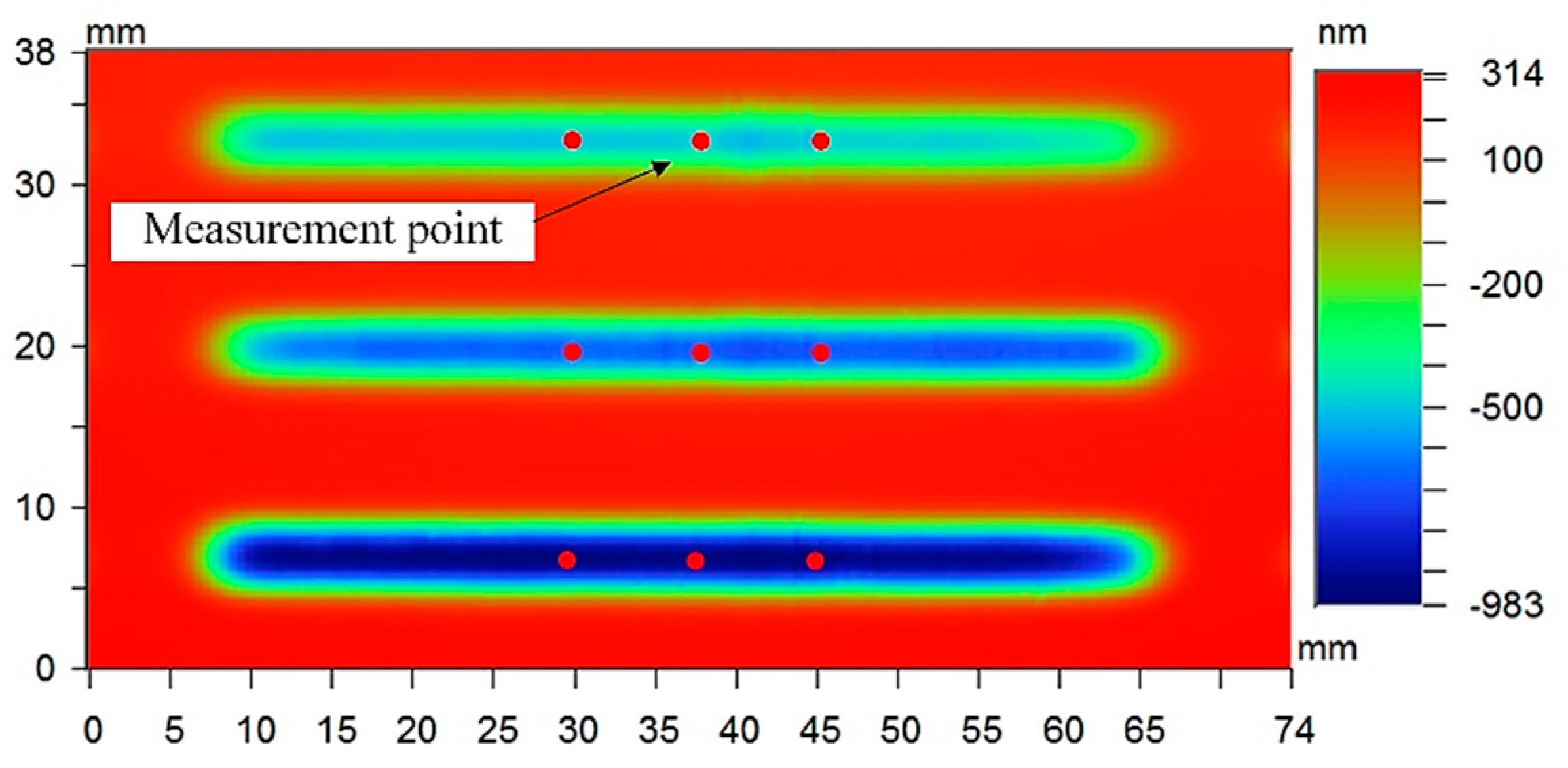
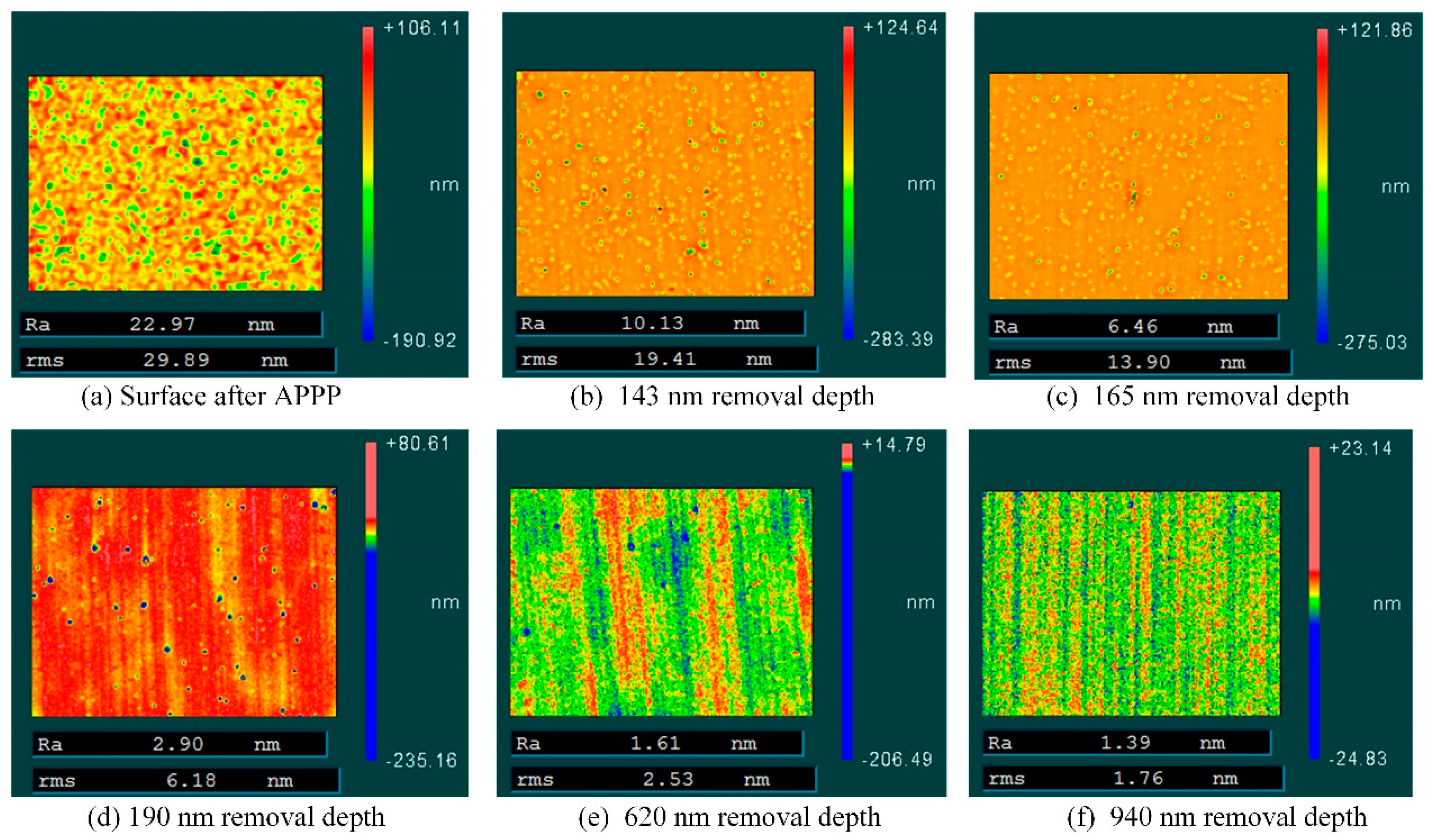
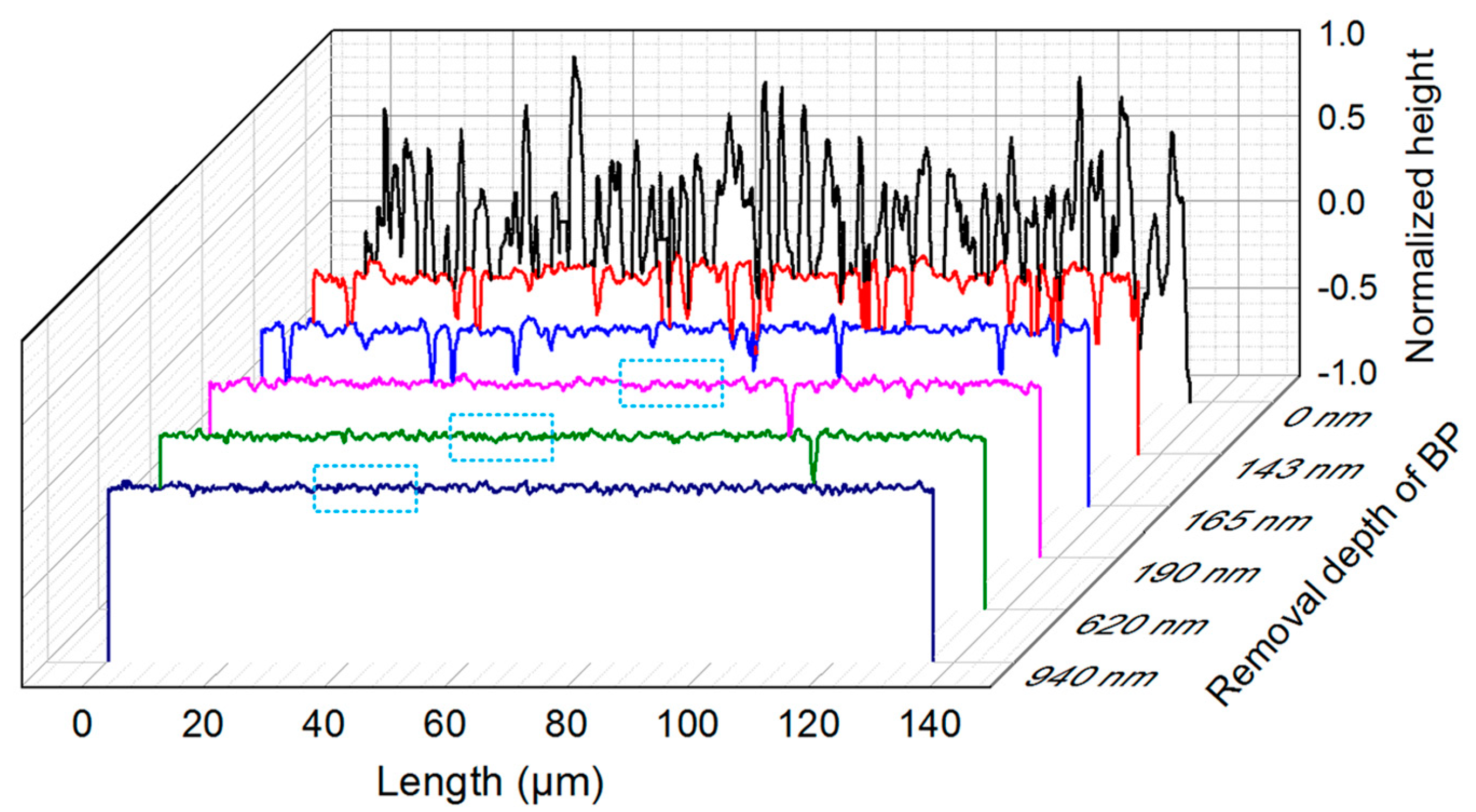
3.2. Finishing of the Plasma Etched Surface Using BP

To investigate the texture evolution in BP, fused silica substrates with different plasma etched texture were prepared. Firstly, the substrates were processed at different removal depth by APPP. The details are given in Table 3. Then, the uniform ‘skin’ over substrates were removed using BP one run and another, in which the polishing removal depth increased until a smooth texture was achieved and unchanged. After each polishing run, the texture was measured using the white light interferometer. Thus, the texture evolution in BP was obtained.
Figure 7 shows the surface texture of substrate F under different removal depth of BP. The original surface after APPP has 22.97 nm Ra, shown in Figure 7a. A series of polishing experiments on the Zeeko machine was conducted with removal depths of 143, 165, 190, 620 and 940 nm and the measurement results are shown in Figure 7b–f. After 143 nm polishing removal, the surface texture becomes relatively flat with the protrusions removed. Besides, many pits etched by APPP appear, which still leaves a high level of roughness. With additional polishing, the number of the etched pits decreases, as shown in Figure 7b–e. Note that, the etched pits almost disappear at removal depth 620 nm, shown in Figure 7e. Finally, the etched pits are eliminated and the typical polished texture is obtained after 940 nm polishing removal, shown in Figure 7f. It can be found that BP smoothed the APPP etched texture by suppressing the protrusions and removing the etched pits.
To elaborate on the texture evolution process more intuitively, Figure 8 presents the cross-section profiles, corresponding to Figure 7. To present the evolution process more clearly, the profile height was normalized. Note that, the cross-section profiles show the surface micro textures. And the depths of the cross-section profiles do not correlate with the removal depth of BP, which is on macroscopic scale. The profile with 0 nm removal of BP has irregular peaks and valleys. After the first polishing run with 143 nm removal, most peaks were removed, leaving an improved texture profile but with many pits. Then, the pits become shallower and disappear gradually with additional polishing. Notably, the local areas avoiding the etched pits in the dotted-line boxes have relatively smooth texture. This indicates that the polishing removal is mainly for removing the etched pits in the surface finishing process.
For the substrate B, the texture smoothing process is faster and needs less polishing removal, as shown in Figure 9. The removal depths after BP were 123, 155, 200 and 520 nm, respectively. After polishing removal of 123 nm, the irregular texture etched by APPP became flat, leaving a few etched pits, similar to Figure 7b. Differently, the etched pits disappeared after only 200 nm polishing removal, shown in Figure 9d. Then, additional polishing did not change the surface texture, which indicates that the polishing removal of less than 200 nm can remove the plasma etched structures to accomplish surface finishing.
Summarizing the measured results of the substrates in Table 3, the correlation between the roughness and the polishing removal depth is given in Figure 10. At the beginning of polishing, the roughness decreases rapidly, which corresponds to removing the protrusions of the etched texture. When the polishing removal exceeds about 200 nm, the roughness decreases slowly and converges to a constant value, about 1.5 nm Ra. In this process, the etched pits are removed gradually and the smooth surface is achieved finally. More specially, different original texture requires different polishing removal to achieve a smooth surface. For substrates A and B, the APPP etched texture with roughness less than 15 nm Ra can be smoothed to 1.5 nm Ra only after 200 nm polishing removal. Meanwhile, the other substrates require more polishing to smooth the surface texture. The 1.5 nm Ra, representing the desired smooth texture, can be regarded as the stop condition of the surface finishing by BP. Thus, the relationship between the required BP removal to smooth and the roughness after APPP is obtained, shown in Figure 11.
Furthermore, irregular concavo-convex structures form and the roughness does not change after about 2 um material etched by APPP, according to the findings described in Section 3.1. Therefore, the substrates E and F represent the worst surface textures processed by APPP in the combined process. It can be concluded that the substrate processed by APPP can be certainly smoothed to 1.5 nm Ra with less than one micron of polishing removal by BP.

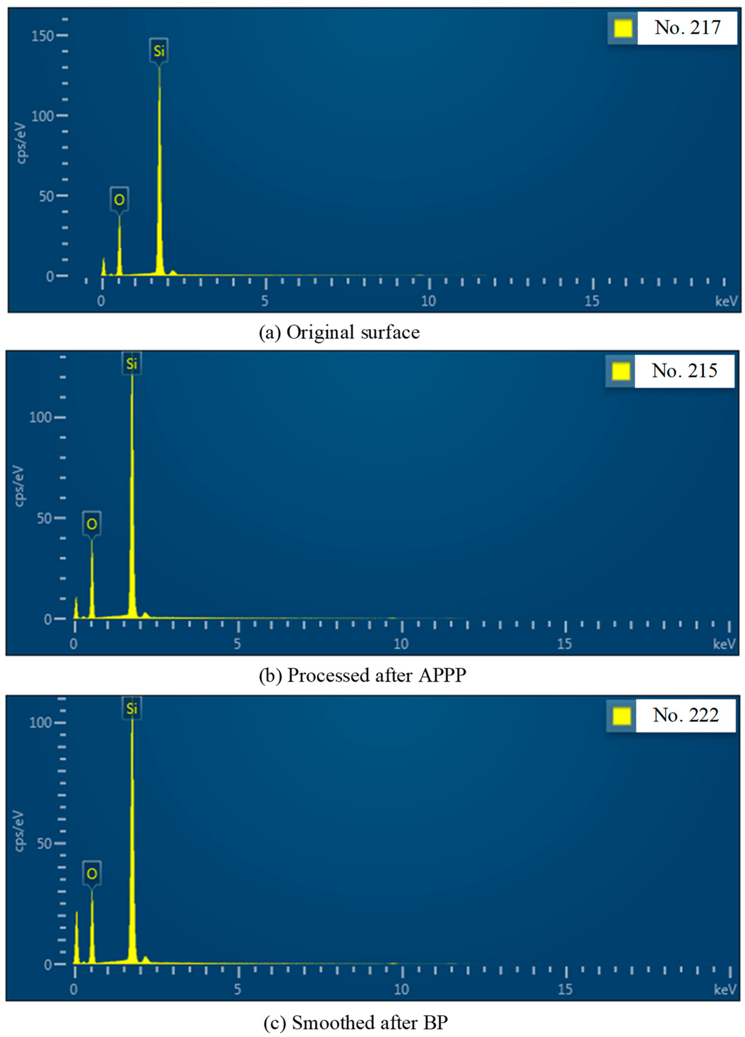
3.3. Chemical Composition Analysis in the Combined Process

To investigate the chemical composition on substrate surface in the combined process, three substrates were analyzed, as shown in Figure 12. Figure 12b presents the surface processed after APPP. The SEM result is similar to Figure 5i, showing a typical plasma-etched texture. Figure 12c is the surface smoothed after BP. It can be seen that the etched texture is totally removed. Energy dispersive spectroscopy (EDS) was also conducted on the three surfaces, as shown in Figure 13. The energy distribution on the three surfaces is basically the same. The two peaks correspond to Si and O. Table 4 gives the atom percent of different elements. The atom percent of O is about twice that of Si, indicating that the main component is SiO2. Overall, in the whole combined process, the chemical component on substrate surface keeps constant.

4. Discussion

The results in Section 3 provide the experimental change law of the surface roughness in the combination process. In practical machining of optical mirrors or windows, the roughness after a certain removal depth of APPP can be predicated using Figure 6, then the required removal depth of BP can be obtained based on Figure 11. In this way, there is no need to measure the surface roughness after APPP, which speeds up the end-to-end process. It is also important to point out that the relationship in Figure 11 is related to substrate material, pre-preparing processing and ambient effects. These conditions were kept consistent in this study, which makes the relationship significant and predictive. When the conditions change, the relationship should be calibrated based on new experiments. Since the chemical etching mechanism is the same in APPP, the surface characteristics should be similar under different conditions. Thus, the change tendency of the relationship can be the same.
As shown in Figure 7b and Figure 9b, the etched pits become visible after slight polishing and remain through subsequent polishing. The subsequent polishing is for removing these etched pits, which affects the finishing efficiency. Thus, the formation mechanism, the related influence factors and the characteristics of the etched pits should be investigated in the future work.
In another respect, APPP opens the micro-cracks and generates the etched pits, similar to the effect of hydrofluoric acid [30]. Because the chemical etching does not induce new SSD, the etched pits should be related to the original sub-surface quality. Hence, the combination of APPP and BP may provide an alternative observation method for sub-surface quality.

5. Conclusions

This paper focuses on the surface texture evolution in the combination of APPP and BP. The fused silica substrates were processed by APPP and then smoothed by BP, the surface texture and roughness in the process were presented and analyzed. The main conclusions are drawn as follows:
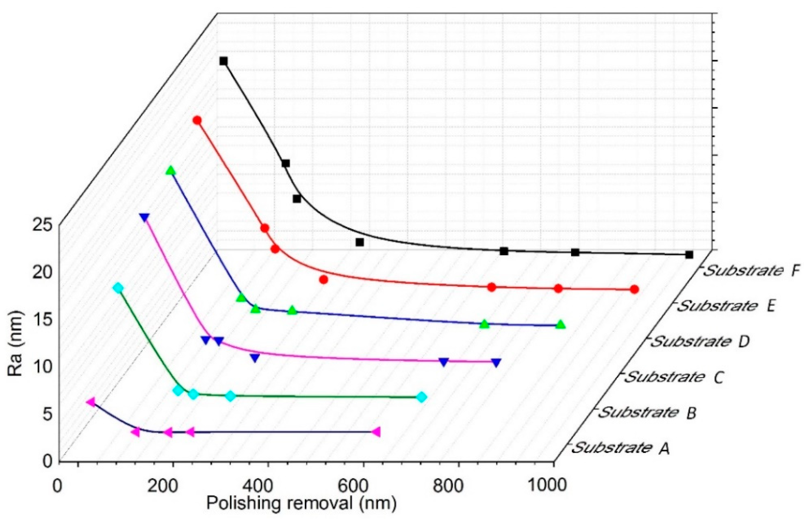
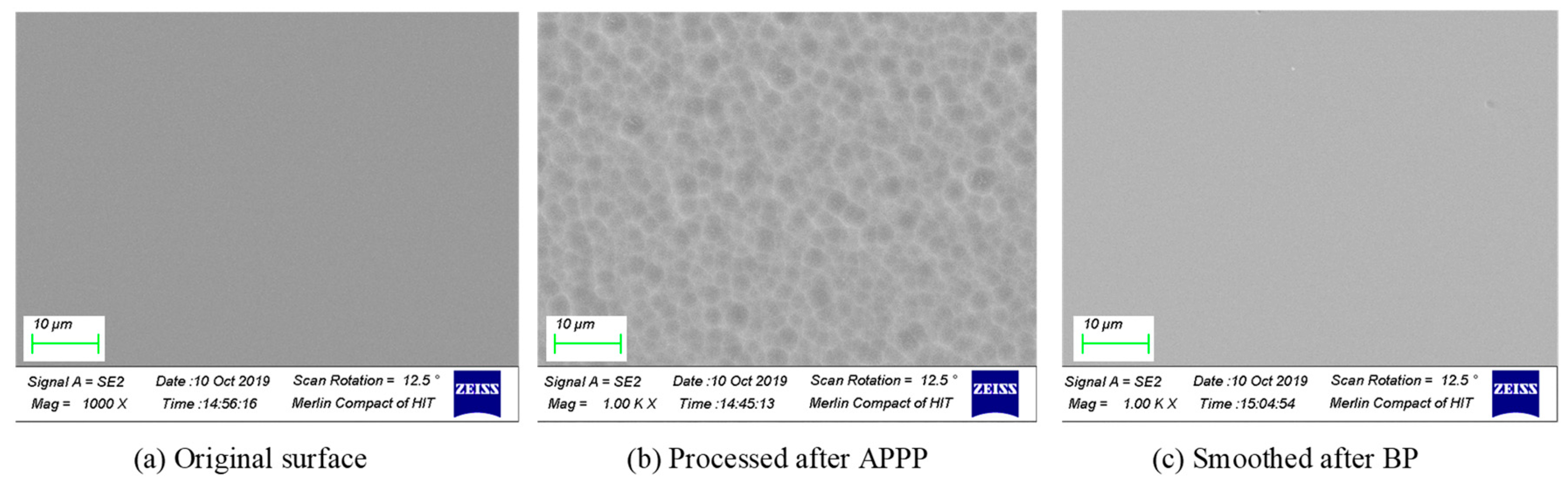
  • The surface texture development in APPP can be divided into two stages. In the beginning, separated etched pits appear and become larger and increase in number. With further removal, the etched pits coalesce with each other and irregular convex-concave structures are formed. In addition, the roughness rises rapidly in the first stage and plateaus at about 25 nm Ra.
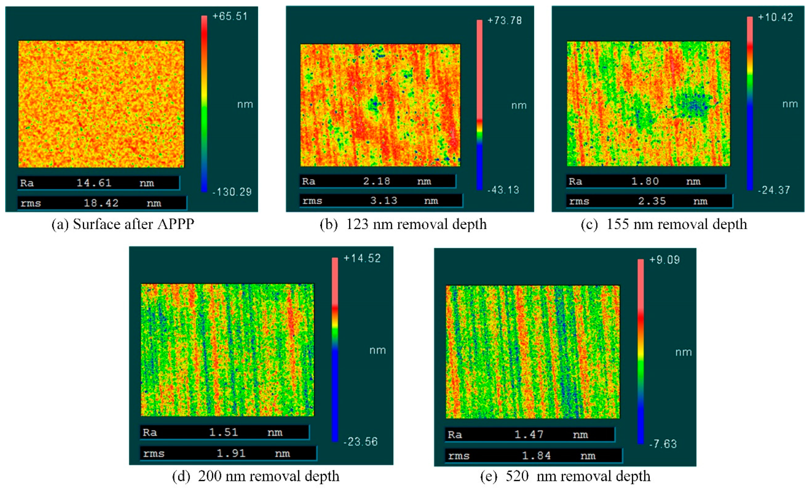
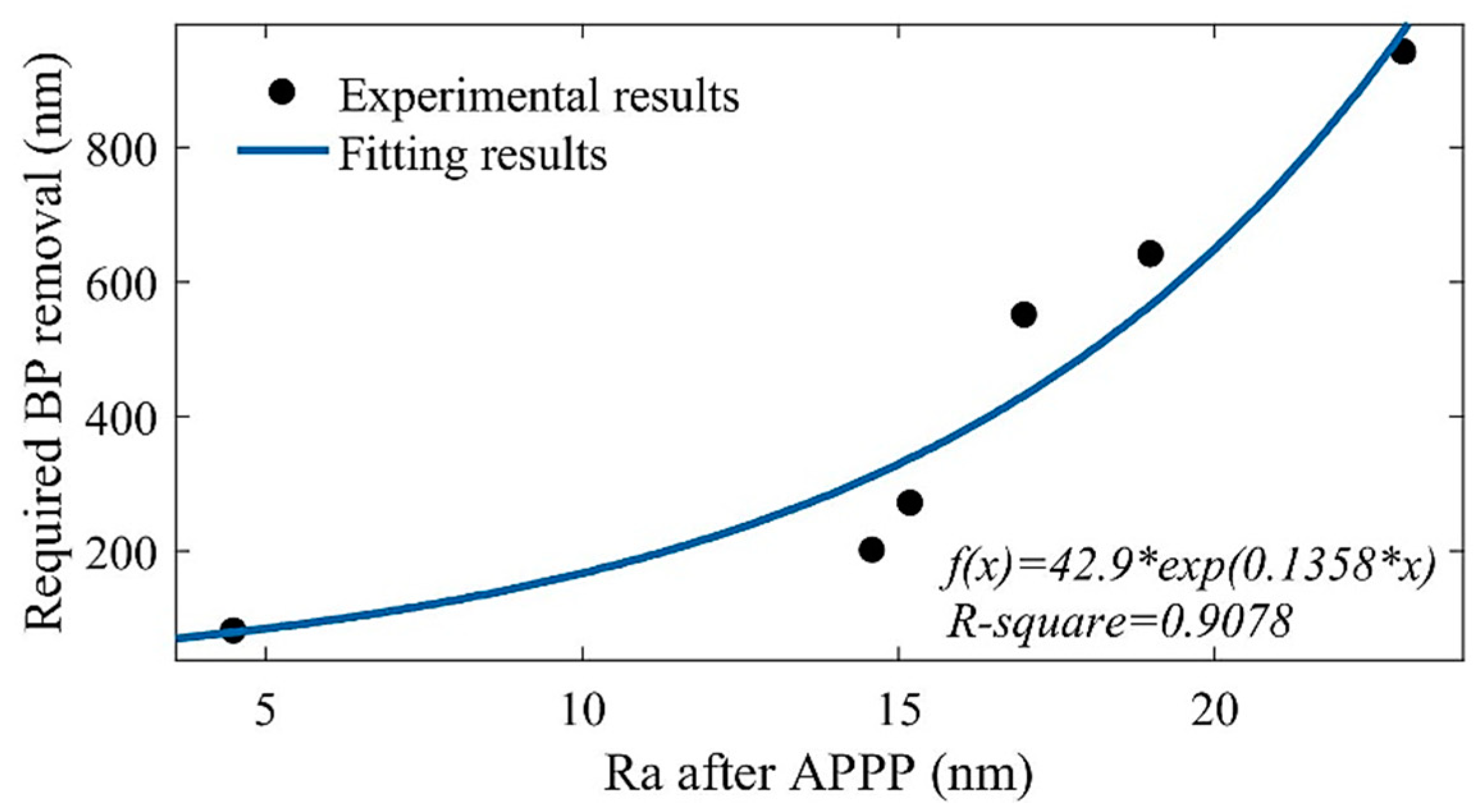
  • For the convex-concave structures on the APPP etched substrates, the protruding peaks can be removed easily with only very modest removal by BP, and the etched pits appeared on the relative flat texture. More additional removal by BP was needed to remove the etched pits, which affects the smoothing efficiency. Overall, the texture etched by APPP can be successfully smoothed to 1.5 nm Ra using BP.

Author Contributions

Conceptualization, X.S.; Investigation, X.S., C.J. and Y.X.; Validation, G.Y. and H.L.; Writing for Original Draft, X.S.; Writing for Review and Editing, D.W., D.L. and B.W.

Funding

This research was funded by National Natural Science Foundation of China (Nos. 51175123, 51105112 and 51905130), National Science and Technology Major Project (No. 2013ZX04006011-205) and China Postdoctoral Science Foundation (Nos. 2019M651276 and 2019TQ0078).

Acknowledgments

The lead author would like to thank the China Scholarship Council (CSC) for its financial support in studying at University of Huddersfield, the National Facility for Ultra Precision Surfaces, North Wales, UK. The UK-based authors acknowledge support from the UK Engineering and Physical Sciences Research Council, the Science and Technology Facilities Council, and the Future Metrology Hub.

Conflicts of Interest

The authors declare no conflict of interest.

References

  1. Campbell, J.H.; Hawley-Fedder, R.A.; Stolz, C.J.; Menapace, J.A.; Borden, M.R.; Whitman, P.K.; Yu, J.; Runkel, M.J.; Riley, M.O.; Feit, M.D.; et al. NIF optical materials and fabrication technologies: An overview. In Proceedings of the Optical Engineering at the Lawrence Livermore National Laboratory II: The National Ignition Facility, San Jose, CA, USA, 28 May 2004; Volume 5341, pp. 102–105. [Google Scholar] [CrossRef]
  2. Bingham, R.G.; Walker, D.D.; Kim, D.H.; Brooks, D.; Freeman, R.; Riley, D. Novel automated process for aspheric surfaces. In Current Developments in Lens Design and Optical Systems Engineering; International Society for Optics and Photonics: San Diego, CA, USA, 2000. [Google Scholar]
  3. Li, H.; Walker, D.; Yu, G.; Zhang, W. Modeling and validation of polishing tool influence functions for manufacturing segments for an extremely large telescope. Appl. Opt. 2013, 52, 5781–5787. [Google Scholar]
  4. Su, X.; Ji, P.; Jin, Y.; Li, D.; Walker, D.; Yu, G.; Li, H.; Wang, B. Simulation and experimental study on form-preserving capability of bonnet polishing for complex freeform surfaces. Precis. Eng. 2019, 60, 54–62. [Google Scholar] [CrossRef]
  5. Cao, Z.C.; Chi, F.C.; Zhao, X. A theoretical and experimental investigation of material removal characteristics and surface generation in bonnet polishing. Wear 2016, 360–361, 137–146. [Google Scholar] [CrossRef]
  6. Cao, Z.C.; Cheung, C.F.; Liu, M.Y. Model-based self-optimization method for form correction in the computer controlled bonnet polishing of optical freeform surfaces. Opt. Express. 2018, 26, 2065–2078. [Google Scholar] [CrossRef]
  7. Harris, D.C. History of magnetorheological finishing. In Proceedings of the Window and Dome Technologies and Materials XII, Orlando, FL, USA, 20 May 2011; Volume 8016, pp. 561–566. [Google Scholar] [CrossRef]
  8. Menapace, J.A.; Dixit, S.N.; Genin, F.Y.; Brocious, W.F. Magnetorheological finishing for imprinting continuous phase plate structure onto optical surfaces. In Proceedings of the Laser-Induced Damage in Optical Materials: 2003, Boulder, CO, USA, 10 June 2004; Volume 5273, pp. 220–230. [Google Scholar]
  9. Xu, M.; Dai, Y.; Xie, X.; Zhou, L.; Peng, W. Fabrication of continuous phase plates with small structures based on recursive frequency filtered ion beam figuring. Opt. Express 2017, 25, 10765–10778. [Google Scholar]
  10. Drueding, T.W.; Fawcett, S.C.; Wilson, S.R.; Bifano, T.G. Ion beam figuring of small optical components. Opt. Eng. 1995, 34, 3565–3572. [Google Scholar] [CrossRef]
  11. Lyu, B.H.; He, Q.K.; Chen, S.H.; Shao, Q.; Chen, Y.; Geng, Z.Y. Experimental study on shear thickening polishing of cemented carbide insert with complex shape. Int. J. Adv. Manuf. Technol. 2019, 103, 585–595. [Google Scholar] [CrossRef]
  12. Li, M.; Lyu, B.; Yuan, J.; Dong, C.; Dai, W. Shear-thickening polishing method. Int. J. Mach. Tools Manuf. 2015, 94, 88–99. [Google Scholar] [CrossRef]
  13. Mori, Y.; Yamauchi, K.; Endo, K. Elastic emission machining. Precis. Eng. 1987, 9, 123–128. [Google Scholar] [CrossRef]
  14. Fähnle, O.W.; Brug, H.V.; Frankena, H.J. Fluid jet polishing of optical surfaces. Appl. Opt. 1998, 37, 6771–6773. [Google Scholar] [CrossRef] [PubMed] [Green Version]
  15. Castelli, M.; Jourdain, R.; Morantz, P.; Shore, P. Rapid optical surface figuring using reactive atom plasma. Precis. Eng. 2012, 36, 467–476. [Google Scholar] [CrossRef]
  16. Shi, B.; Dai, Y.; Xie, X.; Li, S.; Zhou, L. Arc-enhanced plasma machining technology for high efficiency machining of silicon carbide. Plasma Chem. Plasma Process. 2016, 36, 891–900. [Google Scholar] [CrossRef]
  17. Yamamura, K. Improvement of thickness uniformity of quartz crystal wafer by numerically controlled plasma CVM. J. Jpn. Soc. Precis. Eng. Contrib. Pap. 2005, 72. [Google Scholar] [CrossRef]
  18. Mori, Y.; Yamamura, K.; Yamauchi, K.; Yoshii, K.; Kataoka, T.; Endo, K.; Inagaki, K.; Kakiuchi, H. Plasma CVM (chemical vaporization machining): An ultra precision machining technique using high-pressure reactive plasma. Nanotechnology 1993, 4, 225. [Google Scholar] [CrossRef]
  19. Li, N.; Xin, Q.; Zhang, P.; Wang, B. Atmospheric pressure plasma processing of fused silica in different discharge modes. Plasma Sci. Technol. 2015, 17, 567–573. [Google Scholar] [CrossRef]
  20. Dr, T.A.; Boehm, G.; Eichentopf, I.M.; Janietz, M.; Meister, J.; Schindler, A. Plasma jet machining. Vak. Forsch. Und Prax. 2010, 22, 10–16. [Google Scholar] [CrossRef]
  21. Li, D.; Li, N.; Su, X.; Liu, K.; Ji, P.; Wang, B. Characterization of fused silica surface topography in capacitively coupled atmospheric pressure plasma processing. Appl. Surf. Sci. 2019, 489, 648–657. [Google Scholar] [CrossRef]
  22. Li, D.; Li, N.; Su, X.; Liu, K.; Ji, P.; Wang, B. Modelling of removal characteristics and surface morphology formation in capacitively coupled atmospheric pressure plasma processing of fused silica optics. Opt. Mater. Express 2019, 9, 1893–1906. [Google Scholar] [CrossRef]
  23. Subrahmanyan, P.; Gardopee, G.; Verma, Y.; Ning, L.; Yu, T.; Kyler, T.; Fiske, P.; Sommer, P. Rapid fabrication of lightweight SiC aspheres using reactive atom plasma (RAPTM) processing. In Proceedings of the Society of Photo-optical Instrumentation Engineers Conference Series; International Society for Optics and Photonics: San Diego, CA, USA, 2007. [Google Scholar]
  24. Yamamura, K.; Mimura, H.; Yamauchi, K.; Sano, Y.; Saito, A.; Kinoshita, T.; Enso, K.; Mori, Y.; Souvorov, A.; Yabashi, M.; et al. Aspheric surface fabrication in nm-level accuracy by numerically controlled plasma chemical vaporization machining (CVM) and elastic emission machining (EEM). In Proceedings of the X-Ray Mirrors, Crystals, and Multilayers II, Seattle, WA, USA, 24 December 2002; Volume 4782, pp. 265–270. [Google Scholar] [CrossRef]
  25. Mori, Y.; Yamauchi, Y.; Yamamura, K.; Mimura, H.; Saito, A.; Kishimoto, H.; Sekito, Y.; Kanaoka, M.; Souvorov, A.; Yabashi, M. Development of plasma chemical vaporization machining and elastic emission machining systems for coherent X-ray optics. In X-Ray Mirrors, Crystals, and Multilayers; International Society for Optics and Photonics: San Diego, CA, USA, 2001. [Google Scholar]
  26. Arnold, T.; Boehm, G.; Paetzelt, H. New freeform manufacturing chain based on atmospheric plasma jet machining. J. Eur. Opt. Soc. Rapid Publ. 2016, 11. [Google Scholar] [CrossRef]
  27. Su, X.; Xia, L.; Liu, K.; Zhang, P.; Li, P.; Zhao, R.; Wang, B. Fabrication of a large-aperture continuous phase plate in two modes using atmospheric pressure plasma processing. Chin. Opt. Lett. 2018, 16, 102201. [Google Scholar] [CrossRef]
  28. Su, X.; Zhang, P.; Liu, K.; Xia, L.; Li, P.; Zhao, R.; Wang, B. Fabrication of continuous phase plate using atmospheric pressure plasma processing. Int. J. Adv. Manuf. Technol. 2019, 1–12. [Google Scholar] [CrossRef]
  29. Su, X.; Ji, P.; Liu, K.; Walker, D.; Yu, G.; Li, H.; Li, D.; Wang, B. Combined processing chain for freeform optics based on atmospheric pressure plasma processing and bonnet polishing. Opt. Express 2019, 27, 17979–17992. [Google Scholar] [CrossRef]
  30. Carr, J.W.; Fearon, E.; Haack, J.; Hoskins, S.; Hutcheon, I.; Summers, L. Subsurface Structure in Polished Fused Silica and Diamond Turned Single Crystal Silicon; Lawrence Livermore National Lab.: Livermore, CA, USA, 1999. [Google Scholar]
  31. Xin, Q.; Li, N.; Wang, J.; Wang, B.; Li, G.; Ding, F.; Jin, H. Surface roughening of ground fused silica processed by atmospheric inductively coupled plasma. Appl. Surf. Sci. 2015, 341, 142–148. [Google Scholar] [CrossRef]
Figure 1. Combining APPP and BP for freeform generation.
Coatings 09 00676 g001
Figure 2. Experimental setup of APPP.
Coatings 09 00676 g002
Figure 3. Experimental setup of BP.
Coatings 09 00676 g003
Figure 4. Trenches with different removal depth after APPP.
Coatings 09 00676 g004
Figure 5. Surface texture under different removal depth after APPP. (a) original surface; (b) 52 nm; (c) 93 nm; (d) 247 nm; (e) 430 nm; (f) 945 nm; (g) 2.1 μm; (h) 5.2 μm and (i) 12 μm.
Coatings 09 00676 g005
Figure 6. Roughness versus removal depth of APPP.
Coatings 09 00676 g006
Figure 7. Surface texture of substrate F under different removal depth of BP. (a) Surface after APPP; (b) 143 nm; (c) 165 nm; (d) 190 nm; (e) 620 nm and (f) 940 nm.
Coatings 09 00676 g007
Figure 8. Cross-section profiles of substrate F under different removal depth of BP.
Coatings 09 00676 g008
Figure 9. Surface texture of substrate B under different removal depth of BP. (a) Surface after APPP; (b) 123 nm; (c) 155 nm; (d) 200 nm and (e) 520 nm.
Coatings 09 00676 g009
Figure 10. Roughness improvement after different removal depth by BP.
Coatings 09 00676 g010
Figure 11. The required BP removal to smooth the etched texture versus the Ra after APPP.
Coatings 09 00676 g011
Figure 12. SEM images on different substrate surfaces. (a) Original surface; (b) Processed after APPP and (c) Smoothed after BP.
Coatings 09 00676 g012
Figure 13. The energy dispersive spectroscopy on different substrate surfaces. (a) Original surface; (b) Processed after APPP and (c) Smoothed after BP.
Coatings 09 00676 g013
Table 1. Processing parameters of APPP.
RF Power (W)He Flow Rate (sccm)CF4 Flow Rate (sccm)O2 Flow Rate (sccm)
10012204820
Table 2. Processing parameters of BP.
Bonnet Radius
(mm)
Rotational
Speed (rpm)
Inner Pressure
(bar)
Polishing
Cloth
Offset
(mm)
Precess
Angle (°)
Slurry
4010001Uninap0.515CeO2
Table 3. Substrates details after APPP.
SubstrateABCDEF
APPP removal depth (μm)0.150.40.61.02.110.4
Ra after APPP(nm)4.514.615.21719.022.9
Table 4. Chemical component on different substrate surfaces.
SubstrateOriginal SurfaceProcessed after APPPSmoothed after BP
Atom percent of Si (%)37.4837.0837.55
Atom percent of O (%)62.5262.9262.45

