1. Introduction
The thickness of a coating layer can be measured with various methods, including a crater grinding test, an electrical resistance measurement, an optical cross-section measurement, and a razor blade indentation test. Among such conventional methods, crater grinding and razor blade indentation tests are destructive methods to break a coating layer [
1,
2]. Electrical resistance measurement is a nondestructive method and the substrate should be conductive and flat [
3]. This method is widely used to measure the thickness of paint coating on steel. Optical cross-section measurement is done with an optical microscope. For the measurement, a coated specimen cut in the cross-sectional direction should be prepared [
4]. Energy dispersive X-ray spectroscopy is used to measure the thickness of an electrodeposited coating layer as another technique [
5]. The X-ray spectroscopy technique enables determination of the thickness and composition of electrodeposited thin film. However, the method using X-ray spectroscopy is more expensive than the other ones described above.
Electrodeposited coating used for automotive components maintains the variance of its thickness [
6,
7]. Initial coating thickness in a single specimen ranges from a few microns to a few dozen microns. In order to minimize the effect of this variance on wear lifetime, it is necessary to measure coating thickness in the vicinity of a contact region after wear testing. However, it is difficult to use conventional methods that measure coating thickness near a contact region or on a worn surface.
Electrical contact resistance is a useful indicator to check the electrical contact rate on conductive materials. Thus, it has been used to determine the fretting lifetime of electrical connectors [
8,
9]. Electrical contact resistance in an electrical connector was found to be increased with respect to fretting cycle. Failure of an electroplated coating on an electrical connector was defined as the cycle at which the electrical contact resistance reached a critical value. A four-wire resistance measurement was used with an electroplated connector during a fretting test. Meanwhile, electrical contact conductance, the inverse quantity of electrical contact resistance, may be used to distinguish between conductive and nonconductive regions in a coated system; for example, the contact between a metal and a nonconductive material has almost zero electrical contact conductance, while metal-to-metal contact maintains a nonzero value. The actual electrical contact conductance between metals can be affected by the real area of contact consisting of a large number of microcontacts [
10]. Microcontact geometry, the mechanical property of contacting materials, and contact load determine the real area of contact.
In this study, a method to determine the thickness of a nonconductive coating on a metallic substrate was developed. The principle of the developed method is to identify the transition of material by a change in electrical properties. For the purpose of identifying the transition, a slide-hold-slide test using a metallic stylus tip was performed with a worn surface. Vertical displacement of the stylus tip and electrical contact resistance were measured and then analyzed.
2. Materials and Methods
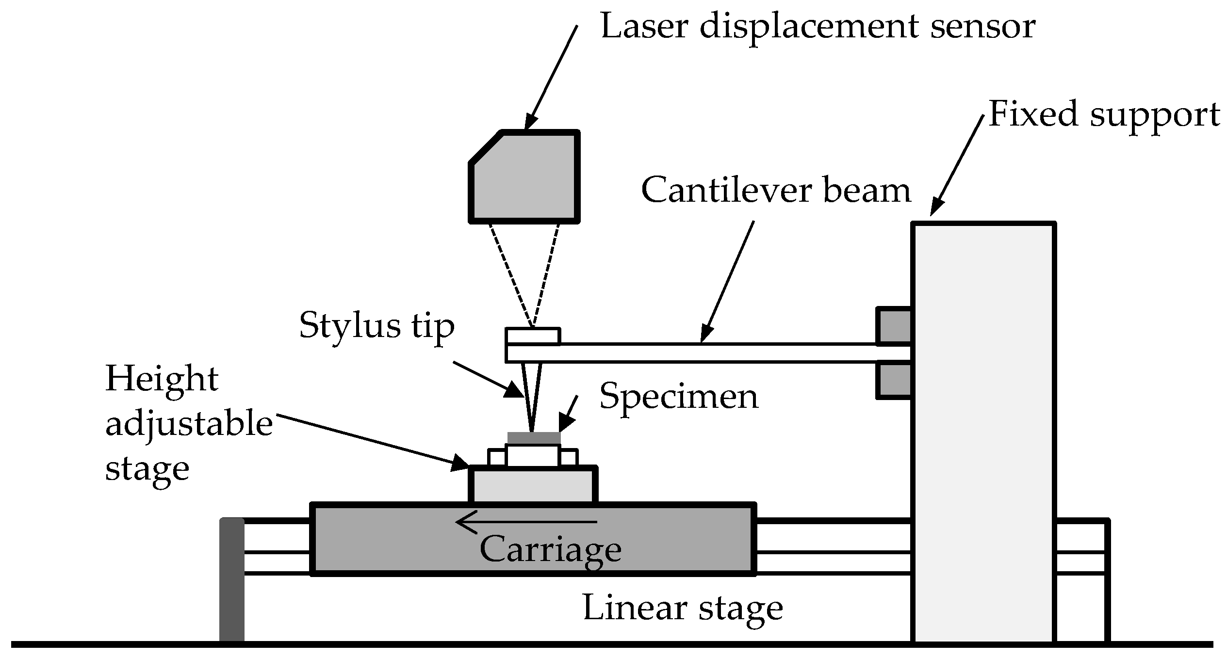
To measure surface profile and electrical contact conductance, a cantilever beam-type tester was developed, as shown in
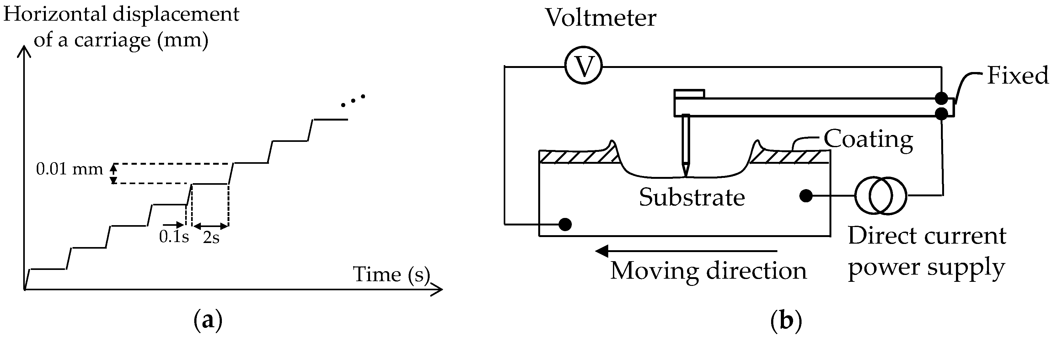
Figure 1. A stylus tip made of stainless steel was fixed on the end of a cantilever beam. The stylus tip, with a diameter of 12 μm, came into contact with the worn surface of the specimen. Contact load was maintained at 8–10 mN during the test to minimize coating removal due to the tip. Vertical displacement of the stylus tip was measured with a laser displacement sensor (Model LK-081, Keyence Corp., Itasca, IL, USA). The specimen was mounted on a height-adjustable stage attached on the carriage of a linear stage. The carriage moved the specimen in the horizontal direction. The horizontal motion of the specimen is presented in
Figure 2a. The specimen was permitted to slide at a sliding velocity of 0.1 mm/s. After 0.01 mm of sliding, the specimen was held for 2 s to measure electrical contact resistance. Then, the specimen was slid to the next position (so-called slide-hold-slide test).
In order to measure electrical contact resistance between the tip and the worn surface, a 4-wire resistance method was used, as shown in
Figure 2b. A resistance meter maintained a resolution of 0.1 Ω and a sampling rate of 1 Hz. Measurement was carried out at a test current of 0.1 mA DC and an open circuit voltage of about 3.08 V DC. After measurement, electrical contact conductance was calculated and recorded along with the vertical displacement of the tip.
If the metallic tip is placed on a coating layer that is nonconductive, electrical contact conductance is zero. If the metallic tip comes into contact with the conductive substrate, electrical contact conductance becomes nonzero. That is, at the transition from the coating to the substrate, the conductance changes from zero to nonzero. The relative vertical displacement of the tip at the transition of the conductance can be used to determine the thickness of a nonconductive coating.
3. Results and Discussion
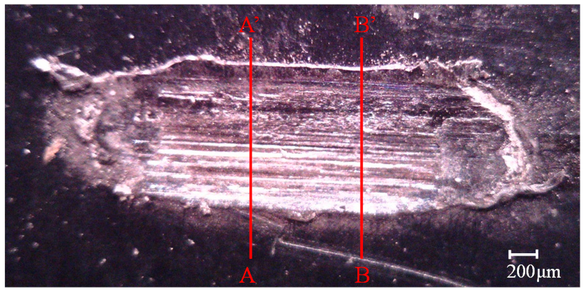
Slide-hold-slide tests using a mechanical stylus tip were conducted at 25 °C and 60% relative humidity (RH). Relative displacement was imposed between a stainless steel stylus tip and a worn surface in the cross-sectional direction, as shown in
Figure 3. The worn surface was obtained via a sliding test with electrodeposited high-strength steel. A test apparatus used for the worn surface was described in the author’s earlier paper [
11]. A Φ5 mm AISI52100 ball was slid on a coated steel specimen at the displacement amplitude of 0.5 mm, a normal force of 50 N, and a frequency of 1 Hz. Sliding test was terminated at the 800th cycle and a kinetic friction coefficient of 0.5. It was observed that the substrate was roughened and scratches were generated along the sliding path within the contact zone.
After initial sliding, the specimen was held for two seconds to measure the electrical contact resistance between the tip and the surface of the specimen. Then, it was permitted to move to the next location (a sliding distance of 0.02 mm with a sliding velocity of 0.2 mm/s). During sliding, the vertical displacement of the tip was measured. Tip vertical displacement and electrical contact resistance were used to calculate the surface profile and electrical contact conductance, respectively.
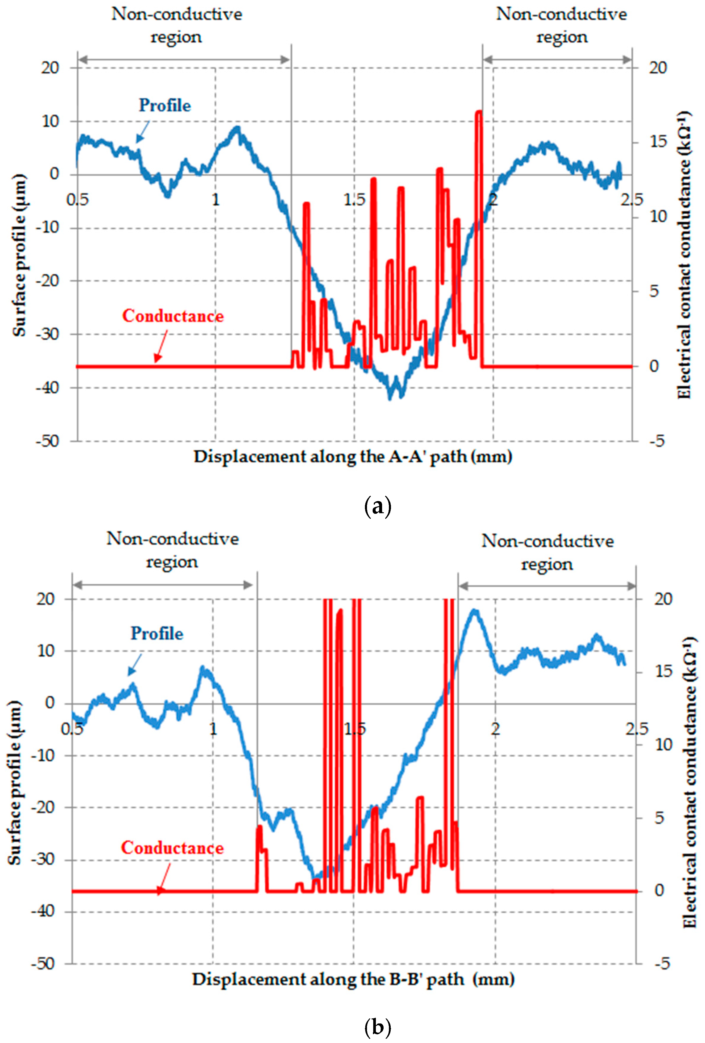
Figure 4 shows the surface profile and electrical contact conductance in the cross-sectional direction. Values of the surface profile close to zero corresponded to the nondamaged coating surface. That is, because the coating was nonconductive, electrical contact conductance remained zero at the contact between the tip and the surface of the coating. The variance in the profile was attributed to coating roughness. Within the displacement range of 1.2–2.0 mm, the profile remained below zero, indicating a worn area. The worn area included the worn coating region and the substrate region. If the metallic tip contacted a coating layer remaining in the worn area, electrical contact conductance was zero. Once the tip came into contact with the substrate surface, electrical contact conductance increased. As shown in
Figure 4a, the nonzero electrical contact conductance appeared at a displacement of 1.28 mm in the A–A’ direction. Electrical contact conductance was observed in various ranges according to location. Assuming Hertz contact between a tip with a radius of 6 μm and a flat steel surface, real contact radius (
a) was approximated as 0.7 μm at a normal force of 8 mN [
12]. Electrical contact resistance,
Rc, was calculated as 0.1 Ω (that is,
Rc = ρ/2
a, where ρ is resistivity [
13]). Electrical contact conductance was then determined as 10 Ω
−1. As shown in
Figure 4, some electrical contact conductance values were found to be much higher than 10 Ω
−1. This meant that some plastic deformations might occur, leading to higher contact area and lower electrical resistance.
At a displacement of 1.28 mm, the surface profile value was −10 μm and the conductance changed from zero to 1 kΩ
−1. In this study, it is proposed that coating layer thickness is defined as the wear depth at the transition of electrical contact conductance. In
Figure 4a, two values corresponding to coating thickness can be obtained from the displacements of 1.28 mm and 1.96 mm. Thus, the average value was used for the coating thickness.
Figure 4b shows the surface profile and electrical contact conductance along the B–B’ direction. The profile values were close to zero in the displacement range from 0.5–1.0 mm, while the values were about 10 μm in the range of 2.0 –2.5 mm. This was associated with the waviness of the coating surface. When electrical contact conductance became nonzero, the surface profile value was −16.24 μm at a displacement of 1.14 mm. Meanwhile, when electrical conductance became zero from a nonzero state, the surface profile was found to be 1.83 μm. Note that the surface profile for the nondamaged coating surface was 10 μm for a displacement of greater than 2.0 mm. This meant that coating thickness can be calculated as the difference (i.e., 8.17 μm).
Table 1 shows the calculated coating thickness in both directions, ranging from 10.11 μm to 12.21 μm.
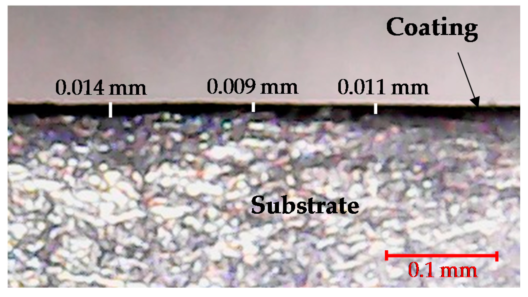
In order to identify the small variance in the calculated coating thickness, the cross-sectional area of a specimen was captured with an optical microscope.
Figure 5 shows the cross-sectional area of the nondamaged electrodeposited substrate. The dark area indicates an electrodeposited coating layer, and the bright area shows the substrate made of high-strength steel, identified from the image with coating thickness ranging from 9 μm to 14 μm. The calculated coating thickness in
Table 1 is included in the measured thickness range.
In this study, a comparison was made between the initial coating thickness of the unworn specimen and the calculated one on the worn surface. Note that there remains difficulty in precisely measuring coating thickness on the path of a slide-hold-slide test. Thus, further work needs to include direct comparisons between coating thicknesses at the same location.
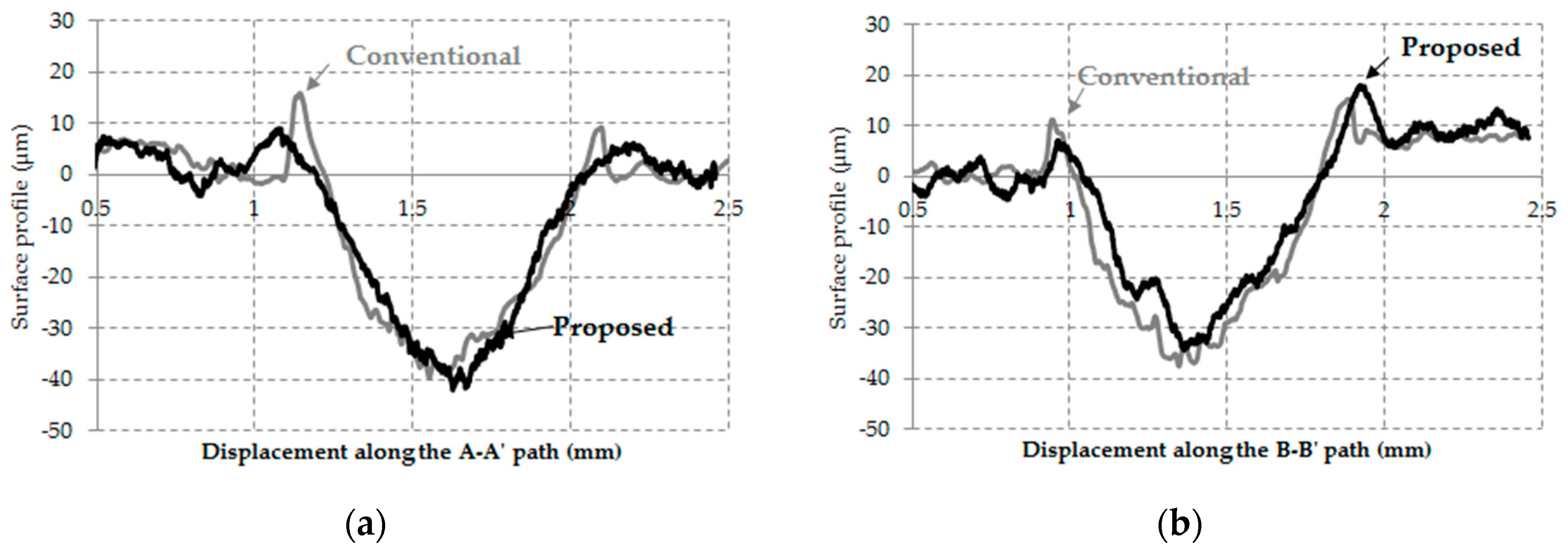
Surface profile was measured with a metallic stylus tip with a diameter of 12 μm. A conventional mechanical stylus tip provides smaller diameter for accurate profile measurement.
Figure 6 shows surface profiles with a conventional mechanical stylus method (Mitutoyo SJ-210, tip diameter of 4 μm; Mitutoyo Corp., Takatsuku, Kawasaki, Japan). It was seen that surface profiles measured by the proposed method were in good agreement with those by the commercial surface profile tester. The small difference in surface profile was attributed to the diameter of the stylus tip; note that the stylus tip in the proposed method had a diameter of 12 μm, bigger than the tip of a commercial mechanical stylus.
In this study, an electrodeposited coating was selected to verify the proposed method. Further work needs to include measurements with other coatings. Additionally, a metallic stylus tip with a diameter of 12 μm was used. A smaller stylus tip will provide more accurate measurement of surface profile. In addition, the surface of the tip needs to be treated for good anticorrosive property and against the growth of thin oxide films at the contact. In order to obtain high reliability, various paths per specimen will be taken into account. For the purpose of reducing conductivity signal noise, a forward-backward scanning mode will be considered in future work. The proposed method may enable measurement of the layer thickness of multilayer coatings containing different materials. Therefore, an attempt to determine multilayer coating thickness will be made with the proposed method.


