Article

Effects of Decaphenylcyclopentasilane Addition on Photovoltaic Properties of Perovskite Solar Cells

1
Department of Materials Science, The University of Shiga Prefecture, 2500 Hassaka, Hikone, Shiga 522-8533, Japan
2
Frontier Materials Laboratories, Osaka Gas Chemicals Co., Ltd., Osaka 554-0051, Japan
*
Author to whom correspondence should be addressed.
Coatings 2018, 8(12), 461; https://doi.org/10.3390/coatings8120461
Submission received: 8 November 2018 / Revised: 4 December 2018 / Accepted: 10 December 2018 / Published: 13 December 2018

Abstract

:
Perovskite solar cells, in which decaphenylcyclopentasilane (DPPS) layers were formed on the surface of the perovskite layer, were fabricated, and the influence on photovoltaic characteristics was investigated. The devices were fabricated by a spin-coating technique, and the surface morphology and crystal structures were investigated by scanning electron microscopy and X-ray diffraction. By adding the DPPS, the fill factor and open circuit voltage were increased, and the photoelectric conversion efficiency was improved. A stability test in ambient air was carried out for seven weeks, and the photoelectric conversion efficiencies were remarkably improved for the devices with DPPS.

1. Introduction

The organic–inorganic metal halide perovskite-type solar cells (PSCs) are the most promising devices for renewable energy because they have characteristics of high optical absorption coefficient, long exciton diffusion length, and high carrier mobility [1,2,3,4,5,6]. In recent years, the photoelectric conversion efficiencies of the perovskite solar cells have reached more than 20% [7,8,9,10]. However, perovskite solar cells have several problems, including stability, reproducibility, and abnormal hysteresis [11,12]. In order to solve such problems, researches and developments of perovskite solar cells using polymeric materials have been conducted [13,14,15,16,17,18]. Although 2,2′,7,7′-tetrakis-(N,N-di(p-methoxyphenyl)amine)-9,9′-spirobifluorene (spiro-OMeTAD) are quite often used as a hole transport layer (HTL) for the perovskite cells, there are problems in the cost and stability. Alternative hole transport materials and improvement of the stability have also been reported [19,20,21,22,23]. Recently, many researches on perovskite solar cells using poly(methyl methacrylate) (PMMA) have been reported [24,25,26,27]. By depositing the PMMA layer on the perovskite layer, the PMMA forms a compact layer based on the cross-linking network and protects the device from oxygen and moisture [28]. However, since PMMA is an insulating material, accurate control of film thickness is mandatory. If even just a little thick film is formed, the resistance value increases and the conversion efficiency decreases [27]. Other polymer materials, including polysilane derivatives, have been applied to organic solar cells [29,30,31]. The polysilanes were also applied as a hole transport layer for perovskite solar cells [32,33], and the photovoltaic performance was improved for a device using decaphenylcyclopentasilane (DPPS). However, there are few reports on the application of the polysilane derivatives to the perovskite photoactive layers [34], except for the hole transport layers [32].
The purpose of the work presented was to investigate photovoltaic properties of CH3NH3PbI3 (MAPbI3) perovskite-type solar cells with DPPS prepared by a simple spin-coating technique in ambient air. There are two advantages for the DPPS. The first is that the DPPS is a p-type semiconductor, and this facilitates hole transfer and rectification at the pn junction. The second is that the DPPS has high stability and acts as a protective layer on the photoactive layer. In previous research, DPPS has been used for the HTLs or additives to the perovskite precursor solutions. Here, the DPPS layer was formed on the perovskite layer during spin-coating of the perovskite layer, which enabled formation of an intermediate layer between the spiro-OMeTAD HTL and the photoactive perovskite layer. The effects of DPPS addition on the top of perovskite layer on the photovoltaic properties and microstructures were investigated using light-induced current density voltage (JV) characteristics, external quantum efficiency (EQE) measurements, XRD, optical microscopy (OM), and SEM.

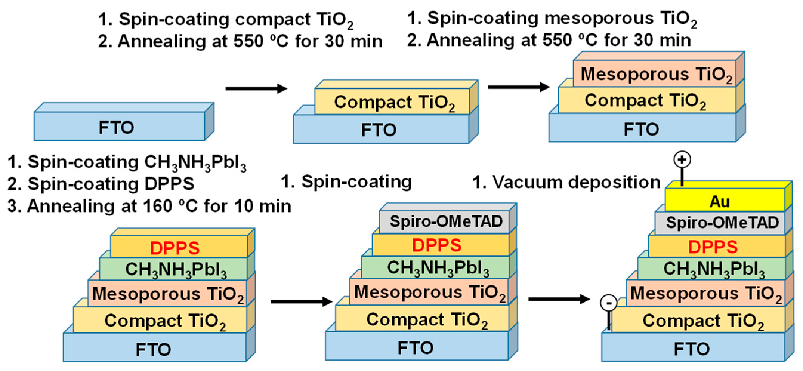
2. Materials and Methods

A schematic illustration of the fabrication process of the proposed MAPbI3/(DPPS) (X mg mL−1) photovoltaic cells is shown in Figure 1. The detailed fabrication process was described in previous reports [35,36,37]. Each layer was formed by the spin-coating method. F-doped tin oxide (FTO) substrates were cleaned using an ultrasonic bath with acetone and methanol and dried under nitrogen gas. Precursor solutions of 0.15 and 0.30 M TiO2, respectively, were prepared from titanium diisopropoxide bis (acetyl acetonate) (0.055 and 0.11 mL, Sigma Aldrich, Tokyo, Japan) with 1-butanol (1 mL, Nacalai Tesque, Kyoto, Japan). The 0.15 M TiO2 precursor solution was spin-coated on the FTO substrate at 3000 rpm for 30 s and annealed at 125 °C for 5 min. This process of 0.30 M solution was performed twice, and the FTO substrate was sintered at 550 °C for 30 min to form a compact TiO2 layer. For the mesoporous TiO2 layer, the TiO2 paste was prepared with TiO2 powder (P-25, Aerosil, Tokyo, Japan) with poly(ethylene glycol) (PEG #20000, Nacalai Tesque, Kyoto, Japan) in ultrapure water [38]. The solution was mixed with acetylacetone (10 μL, Fujifilm Wako Pure Chemical Corporation, Osaka, Japan) and triton X-100 (5 μL, Sigma Aldrich, Tokyo, Japan) for 30 min, and left for 24 h to suppress bubbles in the solution. After that, TiO2 paste was coated on the substrate by spin-coating at 5000 rpm for 30 s. The cells were annealed at 125 °C for 5 min and sintered at 550 °C for 30 min to form the mesoporous TiO2 layer [39]. For preparation of the perovskite compounds, solutions of CH3NH3I (190.7 mg, Tokyo Chemical Industry, Tokyo, Japan), PbCl2 (111.2 mg, Sigma Aldrich, Tokyo, Japan) with the desired molar ratio in N,N-dimethylformamide (0.5 mL, Sigma Aldrich, Tokyo, Japan), was mixed at 60 °C for 24 h. The perovskite precursor solutions were normally spin-coated during the first experiments. During the second and third experiments, an air flow method was applied and spin-coating at 2000 rpm for 60 s was carried out [40]. The standard cells were annealed at 140 °C, and the cells with added DPPS were annealed at 160 °C for 10 min (when the starting materials are CH3NH3I + PbI2, the 100 °C annealing is better, which was also confirmed in the previous works [34,35]; here, the starting materials are 3CH3NH3I + PbCl2, and CH3NH3PbI3 + 2CH3NH3Cl(gas) were formed after the reaction at 140 °C [41]). DPPS (Osaka Gas Chemicals, Osaka, Japan) solutions with different DPPS concentrations were prepared using chlorobenzene (0.5 mL, Fujifilm Wako Pure Chemical Corporation, Osaka, Japan). The concentration of DPPS was adjusted to X = 0–20 mg mL−1. The DPPS solution was dropped onto the perovskite layer during the last 15 s of spin-coating of the perovskite precursor solutions. Then, a HTL was prepared by spin-coating at 4000 rpm for 30 s. For the HTL, a solution of 2,2′,7,7′-tetrakis-(N,N-di(p-methoxyphenyl)amine)-9,9′-spirobifluorene (36.1 mg, Spiro-OMeTAD, Sigma Aldrich, Tokyo, Japan) in chlorobenzene (0.5 mL, Fujifilm Wako Pure Chemical Corporation, Osaka, Japan) was mixed with a solution of lithium bis (trifluoromethylsulfonyl) imide (260 mg, Li-TFSI, Tokyo Chemical Industry, Tokyo, Japan) in acetonitrile (0.5 mL, Sigma Aldrich, Tokyo, Japan) for 24 h. The former solution with 4-tertbutylpyridine (14.4 μL, Sigma Aldrich, Tokyo, Japan) was mixed with the Li-TFSI solution (8.8 μL) for 30 min at 70 °C. All procedures were carried out in air. Finally, Au electrodes were evaporated as top electrodes [36]. Layered structures of the present photovoltaic cells are denoted as FTO/TiO2/MAPbI3/(DPPS)/Spiro-OMeTAD/Au, as shown in a schematic illustration of Figure 1.
The JV characteristics (Keysight B2901A, Keysight Technologies, Santa Rosa, CA, USA) of the photovoltaic cells were measured under illumination at 100 mW cm−2 by using an AM 1.5 solar simulator (San-ei Electric XES-301S, San-Ei Electric Co. Ltd., Osaka, Japan). The solar cells were illuminated through the side of the FTO substrates and the measurement area was 0.090 cm2. The EQE of the cells was also investigated for the same devices (QE-R, Enli Technology, Enli Technology Co. Ltd., Kaohsiung, Taiwan). The microstructures of the perovskite layers were investigated using an X-ray diffractometer (D2 PHASER, Bruker, Billerica, MA, USA), an optical microscope (Eclipse E600, Nikon, Tokyo, Japan), and a scanning electron microscope (JSM-6010PLUS/LA, Jeol, Tokyo, Japan).

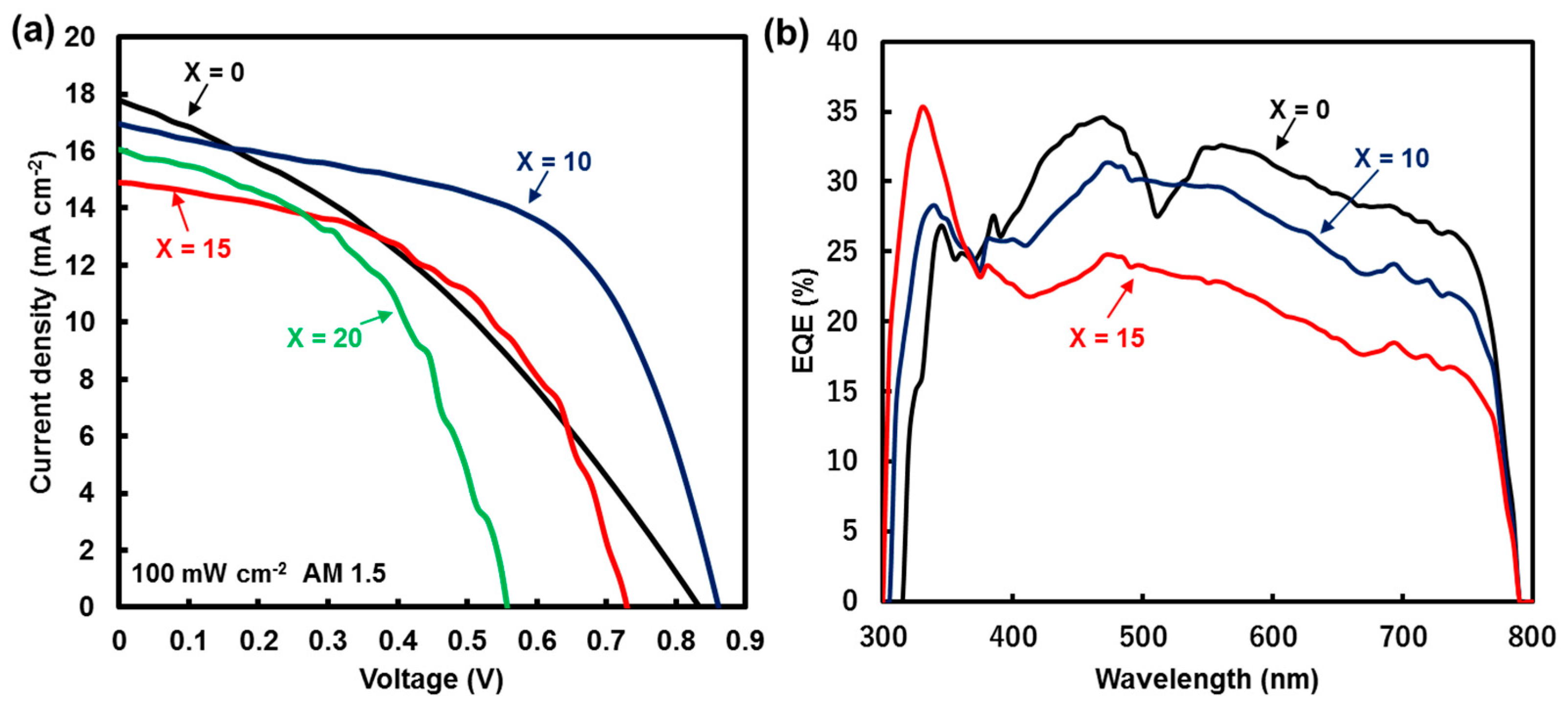
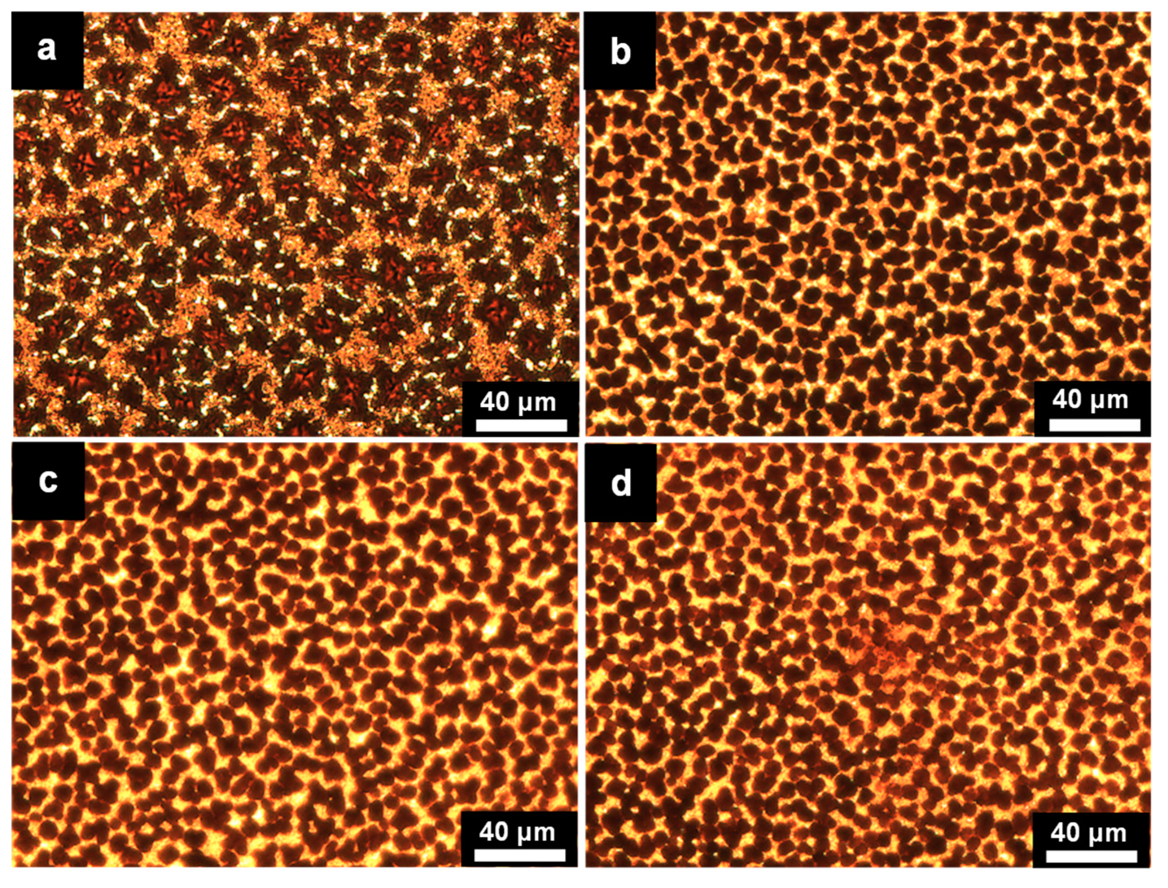
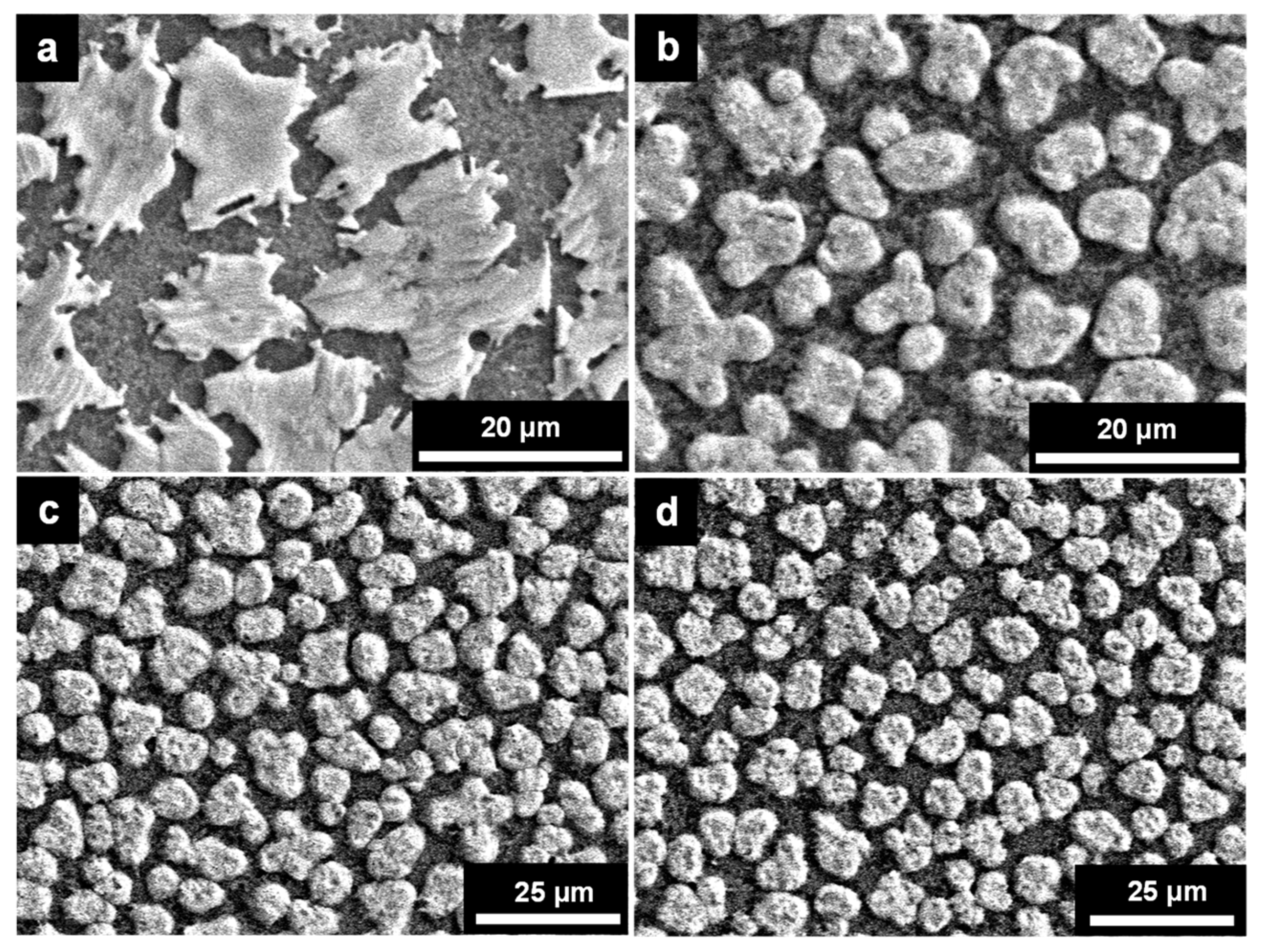
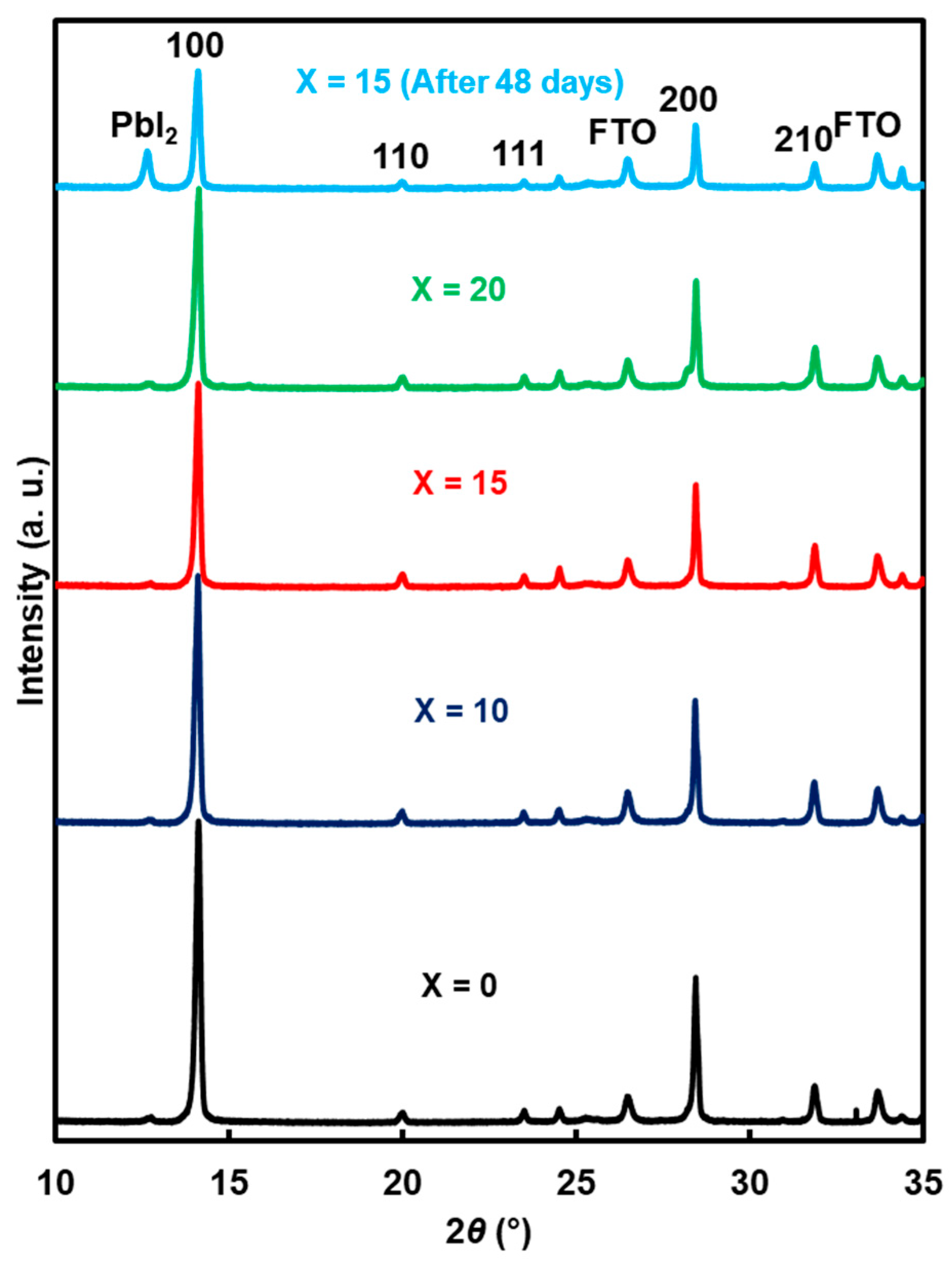
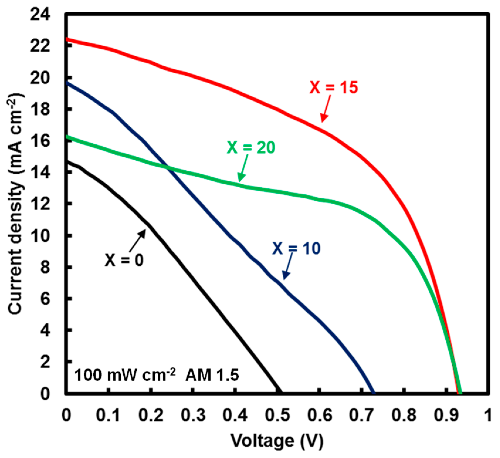
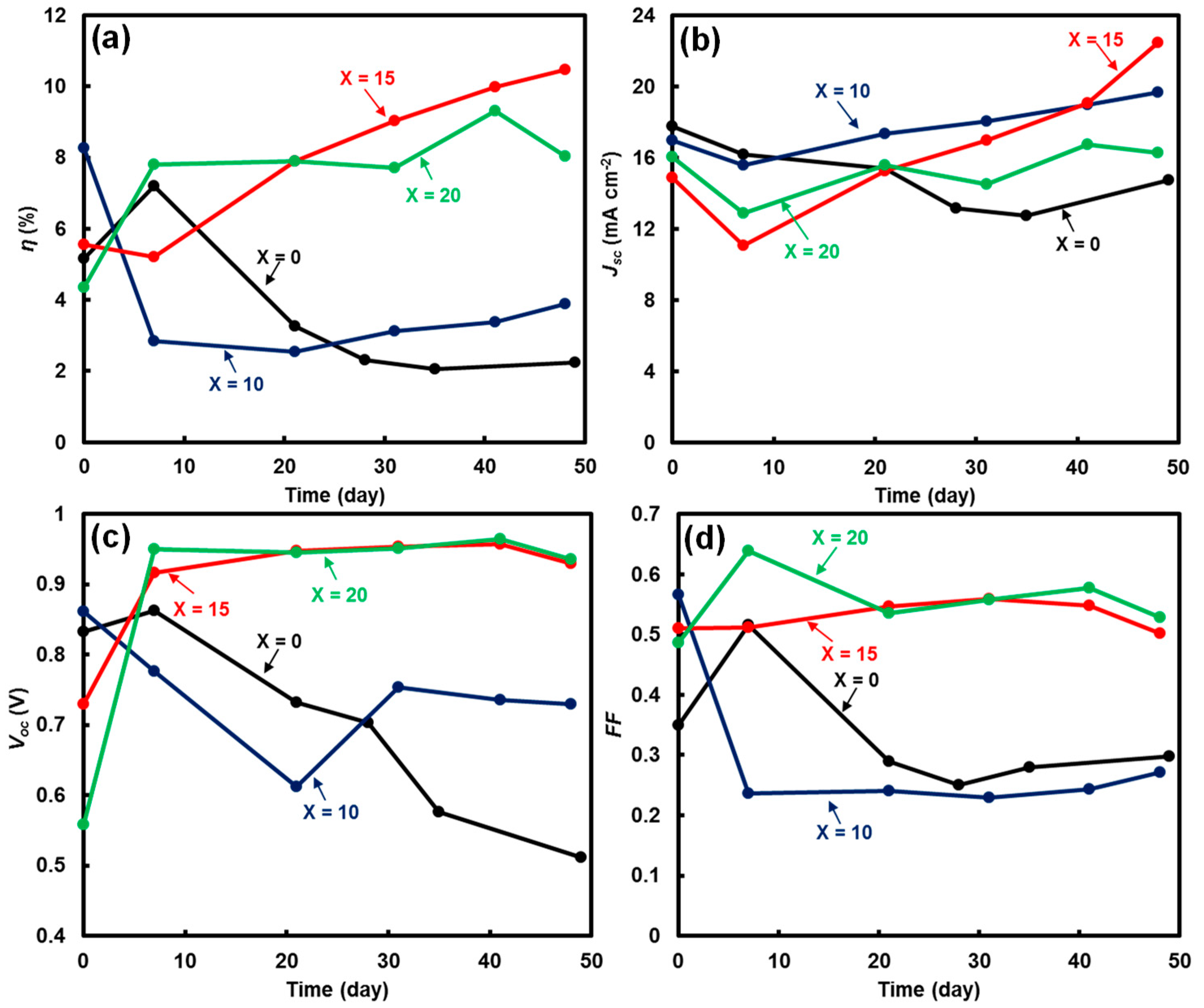
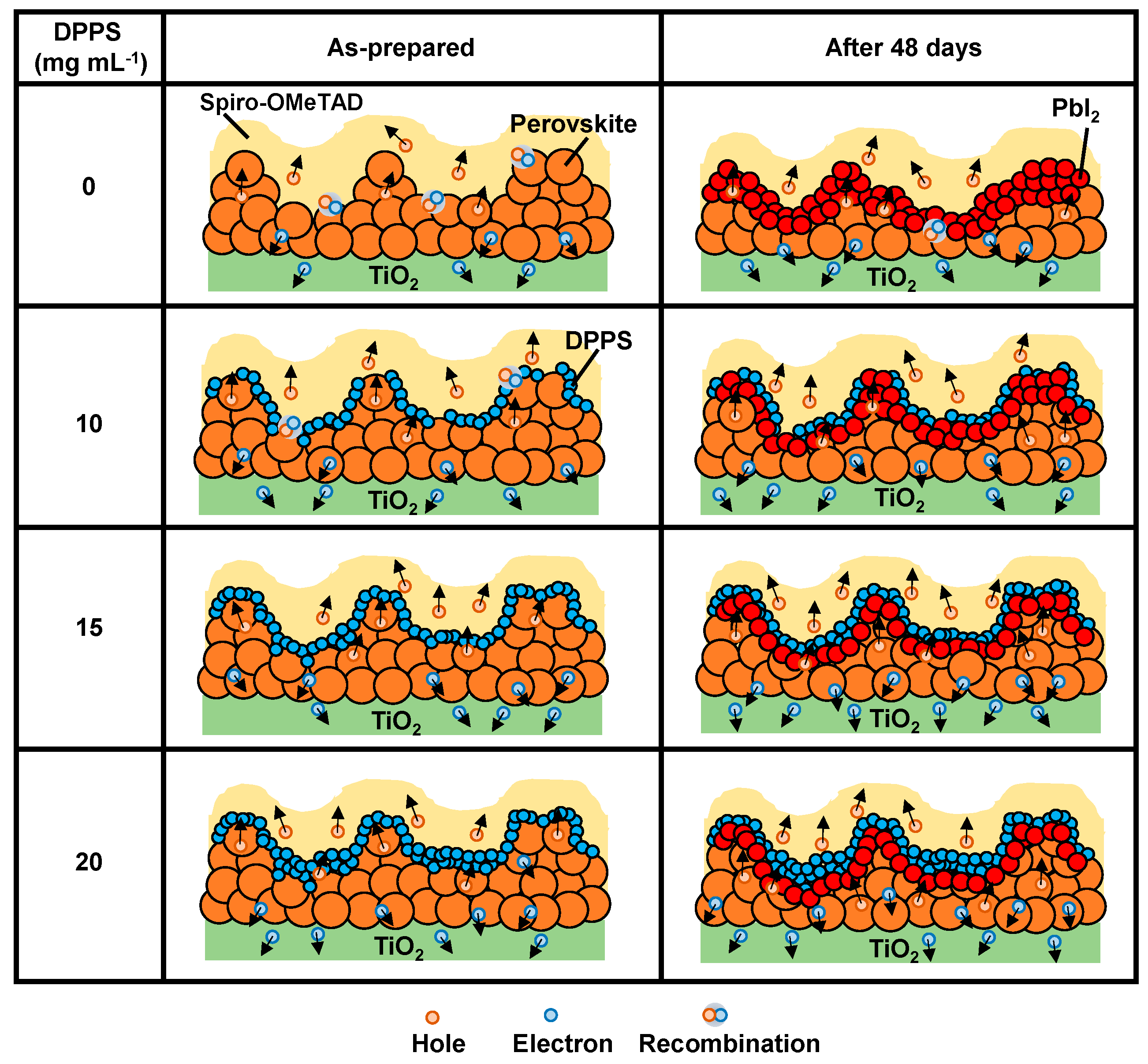
3. Results and Discussion

JV characteristics of the FTO/TiO2/MAPbI3/(DPPS)/Spiro-OMeTAD/Au photovoltaic cells under illumination are shown in Figure 2a. Measured photovoltaic parameters of the MAPbI3/(DPPS) cells are summarized in Table 1. EQE spectra of FTO/TiO2/MAPbI3/(DPPS)/Spiro-OMeTAD/Au cells are shown in Figure 2b. In Figure 2a, the MAPbI3 cell provided the short circuit current density (JSC) of 17.77 mA cm−2, the open circuit voltage (VOC) of 0.833 V, the fill factor (FF) of 0.349, and the conversion efficiency (η) of 5.16%. The perovskite solar cells added with 10 mg mL−1 DPPS showed the highest conversion efficiency of 8.27% and highest average efficiency (ηave) of the four electrodes. In the devices with DPPS added, series resistance (Rs) and shunt resistance (Rsh) were improved, and the FF was improved. The DPPS addition decreased the Jsc, due to an increase in electric resistance by formation of the DPPS film. In Figure 2b, the standard device showed the highest EQE value, which agrees with the highest JSC value in Figure 2a.
Optical microscope images of MAPbI3/(DPPS) (X mg mL−1) perovskite solar cells are shown in Figure 3a–d. Devices with added DPPS had smaller sizes of perovskite crystals, and density of grain distribution was improved compared with the standard device. We suggest that the charge recombination was suppressed by the improvement in density. Therefore, the conversion efficiency was improved in the device to which 10 mg mL−1 DPPS was added.
Figure 4a–d are SEM images of MAPbI3/(DPPS) (X mg mL−1) perovskite solar cells. In the devices to which DPPS was added, the morphology of the perovskite crystal was drastically changed, and the interval of the crystal grains decreased compared with the standard device. We suggest that DPPS affected the crystal growth of the perovskite layer and the surface coverage was improved. The perovskite film also exists in the dark areas of the SEM images and bright areas of the optical microscope images. The crystal grains observed in the SEM images were larger perovskite grains on the perovskite film. Therefore, the TiO2 layers was not exposed to the spiro-OMeTAD.
XRD patterns of MAPbI3/(DPPS) (X mg mL−1) photovoltaic cells are shown in Figure 5. Measured XRD parameters of the MAPbI3/(DPPS) (X mg mL−1) cells are summarized in Table 2. As shown in Figure 5, the DPPS-added devices show almost the same peaks compared with those of the standard device, which indicates that the perovskite structure is preserved. When the devices were measured after about seven weeks, a peak of PbI2 was detected. Crystallite sizes of the perovskite for the cell with 15 mg mL−1 DPPS decreased after 48 days. This is assumed to be due to a part of the perovskite crystals turning into a PbI2 crystal by desorption of CH3NH2 and HI from the CH3NH3PbI3, and the PbI2 crystal precipitating on the surface of the perovskite layer, thereby decreasing the crystallite sizes. This change in crystallite size has little relation to the change in conversion efficiency. Since the PbI2 is a p-type semiconductor, the thin PbI2 precipitation on the surface of the perovskite layer promotes hole transport and also functions as an electron blocking layer. Therefore, the charge recombination was suppressed, and the conversion efficiency was improved.
Figure 6 is the JV characteristics of the FTO/TiO2/MAPbI3/(DPPS)/Spiro-OMeTAD/Au photovoltaic cells after about seven weeks (48 days), and the measured photovoltaic parameters are also summarized in Table 3. As shown in Figure 6, while the conversion efficiency was lowered in the standard device after about seven weeks, the conversion efficiency was improved in the device added with 15 mg mL−1 DPPS. Especially remarkable improvement of JSC and VOC was observed for the device to which 15 mg mL−1 DPPS was added. As listed in Table 1, the device containing 10 mg mL−1 DPPS provided the highest conversion efficiency, which was due to the thin film thickness and low electrical resistance. However, an increasing amount of the PbI2 crystals were formed and the η values decreased after 48 days, which was due to the lower surface coverage of DPPS. On the other hand, the conversion efficiency of the device with 15 mg mL−1 DPPS was lower than that of the standard cell, because of the increased electrical resistance. However, the conversion efficiency improved after 48 days. Since the perovskite layer can be sufficiently covered by the DPPS, decomposition of the perovskite crystals was suppressed, and the p-type semiconducting characteristics of DPPS and PbI2 improved the conversion efficiency.
Figure 7 shows results of the stability measurements of the presented cells up to about 7 weeks. Photovoltaic parameters are also summarized in Table 3. For the DPPS-added devices, the JSC values increased, which is abnormal behavior for the perovskite photovoltaic devices. Improvement or stabilization of the parameters were observed for the devices to which DPPS of 15 mg mL−1 or more was added.
Figure 8 shows schematic models of microstructure, carrier dynamics, and stability of the proposed devices. The standard device without DPPS has defect structures, which cause charge recombination and charge trapping. Although PbI2 precipitation might suppress charge recombination for the standard device after 48 days, the conversion efficiency decreased due to the large amount of precipitated PbI2. For the devices with DPPS, defects of the perovskite layers were reduced by the DPPS layer and charge recombination was suppressed. For the devices with DPPS, after 48 days the formed PbI2 crystals and the DPPS layer acted as an electron blocking layer that promoted charge transfer. As a result, the stability was good and the conversion efficiency improved. For the device with 10 mg mL−1 DPPS, more PbI2 crystals formed over time and the η values decreased after 48 days. This was due to the lower surface coverage of DPPS, which is sensitive to the influence of oxygen and moisture in the air. For devices with 15 and 20 mg mL−1 DPPS, the stability improved because the DPPS layer sufficiently covered the perovskite layer. However, for the device with 20 mg mL−1 DPPS, the electrical resistance increased as the thickness of the DPPS layer increased, and the conversion efficiency was lower than that of the device with 15 mg mL−1 DPPS.

4. Conclusions

Perovskite-based solar cells were fabricated by a spin-coating method, and the effects of DPPS addition on top of the perovskite layers on the photovoltaic properties were investigated. From the results of JV characteristics, FF was improved by adding DPPS. For the device with 15 mg mL−1 DPPS, the JSC and VOC increased, and the photoelectric conversion efficiency was remarkably improved, even after 48 days. Microstructure analysis by optical microscopy and SEM indicated that the morphology of the perovskite crystals was drastically changed, and the grain density was improved. X-ray diffraction analysis showed that the crystal structure did not change, even when DPPS was added to the standard system. The photoelectric conversion efficiency of the device with 15 mg mL−1 DPPS device was improved even after 48 days, which indicates that the charge transfer was accelerated by the PbI2 layer, and that the DPPS layer acted as an electron blocking layer.

Author Contributions

Conceptualization, M.T. and T.O.; Methodology, M.T.; Validation, A.S.; Formal Analysis, M.T.; Investigation, M.T.; Resources, S.F., S.M. and M.O.; Data Curation, M.T. and T.O.; Writing-Original Draft Preparation, M.T.; Writing-Review & Editing, T.O., A.S., S.F., S.M. and M.O.; Visualization, M.T. and T.O.; Supervision, T.O. and A.S.; Project Administration, T.O.; Funding Acquisition, T.O.

Funding

This research was funded by the Super Cluster Program of the Japan Science and Technology Agency (JST).

Conflicts of Interest

The authors declare no conflict of interest.

References

  1. Pan, Y.Y.; Su, Y.H.; Hsu, C.H.; Huang, L.W.; Dou, K.P.; Kaun, C.C. First-principles study on electronic structures of FAPbX3 (X = Cl, Br, I) hybrid perovskites. J. Adv. Nanomater. 2016, 1, 33–38. [Google Scholar] [CrossRef]
  2. Wang, J.F.; Zhu, L.; Zhao, B.G.; Zhao, Y.L.; Song, J.; Gu, X.Q.; Qiang, Y.H. Surface engineering of perovskite films for efficient solar cells. Sci. Rep. 2017, 7, 14478. [Google Scholar] [CrossRef] [PubMed]
  3. Xu, W.; Zheng, L.; Zhang, X.; Cao, Y.; Meng, T.; Wu, D.; Liu, L.; Hu, W.; Gong, X. Efficient perovskite solar cells fabricated by Co partially substituted hybrid perovskite. Adv. Energy Mater. 2018, 10, 1703178. [Google Scholar] [CrossRef]
  4. Li, X.; Zhang, W.; Wang, Y.C.; Zhang, W.; Wang, H.Q.; Fang, J. In-situ cross-linking strategy for efficient and operationally stable methylammoniun lead iodide solar cells. Nat. Commun. 2018, 9, 3806. [Google Scholar] [CrossRef] [PubMed]
  5. Cortecchia, D.; Dewi, H.A.; Yin, J.; Bruno, A.; Chen, S.; Baikie, T.; Boix, P.P.; Gratzel, M.; Mhaisalkar, S.; Soci, C.; et al. Lead-free MA2CuClxBr4-x hybrid perovskites. Inorg. Chem. 2016, 55, 1044–1052. [Google Scholar] [CrossRef] [PubMed]
  6. Gedamu, D.; Asuo, I.M.; Benetti, D.; Basti, M.; Ka, I.; Cloutier, S.G.; Rosei, F.; Nechache, R. Solvent-antisolvent ambient processed large grain size perovskite thin films for high-performance solar cells. Sci. Rep. 2018, 8, 12885. [Google Scholar] [CrossRef] [PubMed]
  7. Klug, M.T.; Osherov, A.; Haghighirad, A.A.; Stranks, S.D.; Brown, P.R.; Bai, S.; Wang, J.T.W.; Dang, X.; Bulovic, V.; Snaith, H.J.; et al. Tailoring metal halide perovskites through metal substitution: influence on photovoltaic and material properties. Energy Environ. Sci. 2017, 10, 236–246. [Google Scholar] [CrossRef]
  8. Yang, W.S.; Park, B.W.; Jung, E.H.; Jeon, N.J.; Kim, Y.C.; Lee, D.U.; Shin, S.S.; Seo, J.; Kim, E.K.; Noh, J.H.; et al. Iodide management in formamidinium-lead-halide-based perovskite layers for efficient solar cells. Science 2017, 356, 1376–1379. [Google Scholar] [CrossRef]
  9. Wang, F.; Bai, S.; Tress, W.; Hagfeldt, A.; Gao, F. Defects engineering for high-performance perovskite solar cells. NPJ Flex. Electron. 2018, 2, 22. [Google Scholar] [CrossRef]
  10. Ng, C.H.; Ripolles, T.S.; Hamada, K.; Teo, S.H.; Lim, H.N.; Bisquert, J.; Hayase, S. Tunable open circuit voltage by engineering inorganic cesium lead bromide/iodide perovskite solar cells. Sci. Rep. 2018, 8, 2482. [Google Scholar] [CrossRef]
  11. Li, N.; Zhu, Z.; Chueh, C.C.; Liu, H.; Peng, B.; Petrone, A.; Li, X.; Wang, L.; Jen, A.K.Y. Mixed cation FAxPEA1-xPbI3 with enhanced phase and ambient stability toward high-performance perovskite solar cells. Adv. Energy Mater. 2017, 7, 1601307. [Google Scholar] [CrossRef]
  12. Zhang, X.; Yin, J.; Nie, Z.; Zhang, Q.; Sui, N.; Chen, B.; Zhang, Y.; Qu, K.; Zhao, J.; Zhou, H. Lead-free and amorphous organic-inorganic hybrid materials for photovoltaic applications: Mesoscopic CH3NH3MnI3/TiO2 heterojunction. RSC Adv. 2017, 7, 37419–37425. [Google Scholar] [CrossRef]
  13. Mali, S.S.; Shim, C.S.; Hong, C.K. Highly stable and efficient solid-state solar cells based on methylammonium lead bromide (CH3NH3PbBr3) perovskite quantum dots. NPG Asia Mater. 2015, 7, e208. [Google Scholar] [CrossRef]
  14. Chen, H.W.; Huang, T.Y.; Chang, T.H.; Sanehira, Y.; Kung, C.W.; Chu, C.W.; Ikegami, M.; Miyasaka, T.; Ho, K.C. Efficiency enhancement of hybrid perovskite solar cells with MEH-PPV hole transporting layers. Sci. Rep. 2016, 6, 34319. [Google Scholar] [CrossRef] [PubMed]
  15. Zuo, L.; Guo, H.; deQuilettes, D.W.; Jariwala, S.; Marco, N.D.; Dong, S.; De Block, R.; Ginger, D.S.; Dunn, B.; Wang, M.; et al. Polymer-modified halide perovskite films for efficient and stable planar heterojunction solar cells. Sci. Adv. 2017, 3, e1700106. [Google Scholar] [CrossRef] [PubMed]
  16. Zhang, S.; Lu, Y.; Lin, B.; Zhu, Y.; Zhang, K.; Yuan, N.Y.; Ding, J.N.; Fang, B. PVDF-HFP additive for visible-light-semitransparent perovskite films yielding enhanced photovoltaic performance. Sol. Energy Mater. Sol. Cells 2017, 170, 178–186. [Google Scholar] [CrossRef]
  17. Chen, Z.; Dong, Q.; Liu, Y.; Bao, C.; Fang, Y.; Lin, Y.; Tang, S.; Wang, Q.; Xiao, X.; Bai, Y.; et al. Thin single crystal perovskite solar cells to harvest below-bandgap light absorption. Nat. Commun. 2017, 8, 1890. [Google Scholar] [CrossRef] [Green Version]
  18. Zhang, H.; Shi, J.; Zhu, L.; Luo, Y.; Li, D.; Wu, H.; Meng, Q. Polystyrene stabilized perovskite component, grain and microstructure for improved efficiency and stability of planar solar cells. Nano Energy 2018, 43, 383–392. [Google Scholar] [CrossRef]
  19. Tavakoli, M.M.; Tavakoli, R.; Prochowicz, D.; Yadav, P.; Saliba, M. Surface modification of a hole transporting layer for an efficient perovskite solar cell with an enhanced fill factor and stability. Mol. Syst. Des. Eng. 2018, 3, 717–722. [Google Scholar] [CrossRef]
  20. Dubey, A.; Adhikari, N.; Mabrouk, S.; Wu, F.; Chen, K.; Yang, S.; Qiao, Q. A strategic review on processing routes towards highly efficient perovskite solar cells. J. Mater. Chem. A 2018, 6, 2406–2431. [Google Scholar] [CrossRef]
  21. Wang, D.; Chan, K.H.; Elumalai, N.K.; Mahmud, M.A.; Upama, M.B.; Uddin, A.; Pillai, S. Interfacial engineering of hole transport layers with metal and dielectric nanoparticles for efficient perovskite solar cells. Phys. Chem. Chem. Phys. 2017, 19, 25016–25024. [Google Scholar] [CrossRef] [PubMed]
  22. Mabrouk, S.; Zhang, M.; Wang, Z.; Liang, M.; Bahrami, B.; Wu, Y.; Wu, J.; Qiao, Q.; Yang, S. Dithieno[3,2-b:2′,3′-d] pyrrole-based hole transport materials for perovskite solar cells with efficiencies over 18%. J. Mater. Chem. A 2018, 6, 7950–7958. [Google Scholar] [CrossRef]
  23. Gaml, E.A.; Dubey, A.; Reza, K.M.; Hasan, M.N.; Adhikari, N.; Elbohy, H.; Bahrami, B.; Zeyada, H.; Yang, S.; Qiao, Q. Alternative benzodithiophene (BDT) based polymeric hole transport layer for efficient perovskite solar cells. Sol. Energy Mater. Sol. Cells 2017, 168, 8–13. [Google Scholar] [CrossRef]
  24. Bi, D.; Yi, C.; Luo, J.; Decoppet, J.D.; Zhang, F.; Zakeeruddin, S.M.; Li, X.; Hagfeldt, A.; Gratzel, M. Polymer-templated nucleation and crystal growth of perovskite films for solar cells with efficiency greater than 21%. Nat. Energy 2016, 1, 16142. [Google Scholar] [CrossRef] [Green Version]
  25. Wang, F.; Endo, M.; Mouri, S.; Miyauchi, Y.; Ohno, Y.; Wakamiya, A.; Murata, Y.; Matsuda, K. Highly stable perovskite solar cells with an all-carbon hole transport layer. Nanoscale 2016, 8, 11882–11888. [Google Scholar] [CrossRef] [PubMed]
  26. Stranks, S.D.; Eperon, G.E.; Grancini, G.; Menelaou, C.; Alcocer, M.J.P.; Leijtens, T.; Herz, L.M.; Petrozza, A.; Snaith, H.J. Electron-hole diffusion lengths exceeding 1 micrometer in an organometal trihalide perovskite absorber. Science 2013, 342, 341–344. [Google Scholar] [CrossRef]
  27. Taguchi, M.; Suzuki, A.; Tanaka, H.; Oku, T. Fabrication and characterization of perovskite solar cells added with MnCl2, YCl3 or poly(methyl methacrylate). AIP Conf. Proc. 2018, 1929, 020012. [Google Scholar]
  28. Wang, F.; Shimazaki, A.; Yang, F.; Kanahashi, K.; Matsuki, K.; Miyauchi, Y.; Takenobu, T.; Wakamiya, A.; Murata, Y.; Matsuda, K. Highly efficient and stable perovskite solar cells by interfacial engineering using solution-processed polymer layer. J. Phys. Chem. C 2017, 121, 1562–1568. [Google Scholar] [CrossRef]
  29. Oku, T.; Nakagawa, J.; Iwase, M.; Kawashima, A.; Yoshida, K.; Suzuki, A.; Akiyama, T.; Tokumitsu, K.; Yamada, M.; Nakamura, M. Microstructures and photovoltaic properties of polysilane-based solar cells. Jpn. J. Appl. Phys. 2013, 52, 04CR07. [Google Scholar] [CrossRef]
  30. Nakagawa, J.; Oku, T.; Suzuki, A.; Akiyama, T.; Yamada, M.; Fukunishi, S.; Kohno, K. Effects of PBr3 addition to polysilane thin films on structures and photovoltaic properties. Green Sustain. Chem. 2017, 7, 20–34. [Google Scholar] [CrossRef]
  31. Oku, T.; Hibi, N.; Suzuki, A.; Akiyama, T.; Yamada, M.; Fukunishi, S.; Kohno, K. Effects of triphenylborane addition to decaphenylcyclopentasilane thin films. Jpn. Soc. Appl. Phys. Conf. Proc. 2015, 3, 011404. [Google Scholar]
  32. Shirahata, Y.; Yamamoto, Y.; Suzuki, A.; Oku, T.; Fukunishi, S.; Kohno, K. Effects of polysilane-doped spiro-OMeTAD hole transport layers on photovoltaic properties. Phys. Status Solidi A 2017, 214, 1600591. [Google Scholar] [CrossRef]
  33. Shirahata, Y.; Oku, T.; Fukunishi, S.; Kohno, K. Fabrication of perovskite-type photovoltaic devices with polysilane hole transport layers. Mater. Sci. Appl. 2017, 8, 209–222. [Google Scholar] [CrossRef]
  34. Oku, T.; Nomura, J.; Suzuki, A.; Tanaka, H.; Fukunishi, S.; Minami, S.; Tsukada, S. Fabrication and characterization of CH3NH3PbI3 perovskite solar cells added with polysilanes. Int. J. Photoenergy 2018, 2018, 8654963. [Google Scholar] [CrossRef]
  35. Oku, T.; Zushi, M.; Imanishi, Y.; Suzuki, A.; Suzuki, K. Microstructures and photovoltaic properties of perovskite-type CH3NH3PbI3 compounds. Appl. Phys. Express 2014, 7, 121601. [Google Scholar] [CrossRef]
  36. Oku, T.; Suzuki, K.; Suzuki, A. Effects of chlorine addition to perovskite-type CH3NH3PbI3 photovoltaic devices. J. Ceram. Soc. Jpn. 2016, 124, 234–238. [Google Scholar] [CrossRef]
  37. Oku, T.; Ohishi, Y.; Suzuki, A.; Miyazawa, Y. Effects of NH4Cl addition to perovskite CH3NH3PbI3 photovoltaic devices. J. Ceram. Soc. Jpn. 2017, 125, 303–307. [Google Scholar] [CrossRef]
  38. Li, Y.; Sun, W.; Yan, W.; Ye, S.; Rao, H.; Peng, H.; Zhao, Z.; Bian, Z.; Liu, Z.; Zhou, H.; et al. 50% Sn-based planar perovskite solar cell with power conversion efficiency up to 13.6%. Adv. Energy Mater. 2016, 6, 1601353. [Google Scholar] [CrossRef]
  39. Ueoka, N.; Oku, T.; Ohishi, Y.; Tanaka, H.; Suzuki, A. Effects of excess PbI2 addition to CH3NH3PbI3-xClx perovskite solar cells. Chem. Lett. 2018, 47, 528–531. [Google Scholar] [CrossRef]
  40. Oku, T.; Ohishi, Y.; Ueoka, N. Highly (100)-oriented CH3NH3PbI3 (Cl) perovskite solar cells prepared with NH4Cl using an air blow method. RSC Adv. 2018, 8, 10389–10395. [Google Scholar] [CrossRef]
  41. Oku, T.; Ohishi, Y. Effects of annealing on CH3NH3PbI3 (Cl) perovskite photovoltaic devices. J. Ceram. Soc. Jpn. 2018, 126, 56–60. [Google Scholar] [CrossRef]
Figure 1. Schematic illustration of the fabrication process of the proposed photovoltaic devices.
Coatings 08 00461 g001
Figure 2. (a) J–V characteristics and (b) External quantum efficiency (EQE) spectra of the CH3NH3PbI (MAPbI3)/dipeptidylpeptidase (DPPS) (X mg mL−1) cells.
Coatings 08 00461 g002
Figure 3. Optical microscope images of the MAPbI3/(DPPS) perovskite solar cells. The concentration of DPPS are (a) 0 mg mL−1, (b) 10 mg mL−1, (c) 15 mg mL−1, and (d) 20 mg mL−1.
Coatings 08 00461 g003
Figure 4. SEM images of the MAPbI3/(DPPS) perovskite solar cells. The concentration of DPPS are (a) 0 mg mL−1, (b) 10 mg mL−1, (c) 15 mg mL−1, and (d) 20 mg mL−1.
Coatings 08 00461 g004
Figure 5. XRD patterns of the MAPbI3/(DPPS) (X mg mL−1) perovskite solar cells.
Coatings 08 00461 g005
Figure 6. JV characteristics of the MAPbI3/(DPPS) (X mg mL−1) perovskite solar cells. The standard system is the device after 49 days, and the system added with DPPS is the device after 48 days.
Coatings 08 00461 g006
Figure 7. Stability measurements of the MAPbI3/(DPPS) (X mg mL−1) perovskite solar cells. (ad) respectively, show photoelectric conversion efficiency (η), short circuit current density (Jsc), open circuit voltage (Voc) and fill factor (FF).
Coatings 08 00461 g007
Figure 8. Schematic illustration of the microstructure, carrier dynamics and stability models for perovskite solar cells with different DPPS concentration.
Coatings 08 00461 g008
Table 1. Measured photovoltaic parameters of MAPbI3/(DPPS) (X mg mL−1) perovskite solar cells.
DPPS X (mg mL−1)JSC (mA cm−2)VOC (V)FFη (%)ηave (%)Rs (Ω cm2)Rsh (Ω cm2)
017.770.8330.3495.162.0728.0105
1016.970.8610.5668.274.339.15245
1514.880.7290.5115.552.589.91314
2016.060.5580.4874.363.639.95186
Table 2. XRD parameters of 100 of the MAPbI3/(DPPS) (X mg mL−1) perovskite solar cells.
DPPS X (mg mL−1)Lattice Constant (Å)Crystallite Size (Å)
06.268536
106.275510
156.271537
206.263464
15 *6.273467
* Measurements of the device after 48 days.
Table 3. Measured photovoltaic parameters of the MAPbI3/(DPPS) (X mg mL−1) perovskite solar cells. The standard device is after 49 days and the device added with DPPS is after 48 days.
DPPS X (mg mL−1)JSC (mA cm−2)VOC (V)FFη (%)ηave (%)Rs (Ω cm2)Rsh (Ω cm2)
014.720.5120.2982.241.9725.467.9
1019.680.7290.2713.903.5718.561.9
1522.450.9290.50210.488.287.17143
2016.260.9350.5288.036.247.59214

