Article

Mechanical Properties of Hydrogen Free Diamond-Like Carbon Thin Films Deposited by High Power Impulse Magnetron Sputtering with Ne

1
Solid State Electronics, The Ångström Laboratory, Uppsala University, SE-75121 Uppsala, Sweden
2
SEG-CEMMPRE-Department of Mechanical Engineering, University of Coimbra, Rua Luis Reis Santos, 3030-788 Coimbra, Portugal
*
Author to whom correspondence should be addressed.
Coatings 2018, 8(11), 385; https://doi.org/10.3390/coatings8110385
Submission received: 2 September 2018 / Revised: 21 October 2018 / Accepted: 26 October 2018 / Published: 29 October 2018

Abstract

:
Hydrogen-free diamond-like carbon (DLC) thin films are attractive for a wide range of industrial applications. One of the challenges related to the use of hard DLC lies in the high intrinsic compressive stresses that limit the film adhesion. Here, we report on the mechanical and tribological properties of DLC films deposited by High Power Impulse Magnetron Sputtering (HiPIMS) with Ne as the process gas. In contrast to standard magnetron sputtering as well as standard Ar-based HiPIMS process, the Ne-HiPIMS lead to dense DLC films with increased mass density (up to 2.65 g/cm3) and a hardness of 23 GPa when deposited on steel with a Cr + CrN adhesion interlayer. Tribological testing by the pin-on-disk method revealed a friction coefficient of 0.22 against steel and a wear rate of 2 × 10⁻¹⁷ m3/Nm. The wear rate is about an order of magnitude lower than that of the films deposited using Ar. The differences in the film properties are attributed to an enhanced C ionization in the Ne-HiPIMS discharge.

1. Introduction

Hydrogen-free diamond-like carbon (DLC) thin films exhibit properties that make them suitable for a wide range of applications, from biomedical implants to engine components. The attractive properties include a high temperature stability, high hardness, and excellent tribological behaviour that is manifested by a low friction coefficient (<0.2) and a wear rate (<10−16 m3/Nm) [1,2,3]. DLC films exhibiting these properties are usually produced by highly ionized physical vapour deposition (PVD) techniques, such as cathodic vacuum arc deposition or pulsed laser deposition. A highly ionized deposition flux provides means for controlling the energy of the depositing atoms that makes it possible to synthesize DLC with desired properties. The resulting DLC films typically exhibit a high density (2.8–3.2 g/cm3) together with a high sp3 bond fraction (75%–90%), which entails a significantly high hardness (>20 GPa). The high density and hardness, however, are accompanied by high levels of compressive stresses (5–10 GPa) [4,5,6]. As a consequence, the film adhesion to the substrate is limited, preventing the growth of thick DLC films (1–3 µm), which are required for wear-resistant applications [7].
Low stress (1–3 GPa) DLC films can be produced by using standard magnetron sputtering such as direct current magnetron sputtering (DCMS). DCMS grown films, however, typically exhibit a much lower mass density (1.8–2.3 g/cm3) and hardness (<20 GPa) [8,9]. The low hardness of the sputtered films entails poor wear resistance since hardness is a crucial factor for the wear resistance of a material [10]. Moreover, owing to a low mass density and low sp3 fraction, the sputter-deposited DLC films suffer from poor thermal stability and undergo graphitization at low temperatures (150–200 °C) [11]. Limited thermal stability and inadequate mechanical strength inhibit the use of sputter-deposited DLC films in high-end wear-resistant and tribological applications. Therefore, the successful implementation of DLC films in these applications requires hard and dense DLC films with low compressive stresses and high thermal stability, which is not possible with state-of-the-art methods.
Compressive stresses in DLC films originate from the sub-surface implantation (also known as subplantation) of energetic depositing carbon ions which are essential for the formation of dense DLC films [11,12]. The subplantation process is followed by a thermal spike which may lead to stress relaxation with depositing ion energies exceeding 100 eV [13]. For a low sp3 DLC structure, the stress relaxation occurs at the expense of mass density which deteriorates the mechanical properties. On the other hand, sp3 rich DLC films do not undergo any substantial structural changes upon thermal spike induced stress relaxation [14]. The authors previously exploited the ion-induced stress relaxation in the post-thermal spike regime using pulsed ionized flux to produce high density and low compressive stress DLC films [15]. Pulsed ionized deposition fluxes were generated using high power impulse magnetron sputtering (HiPIMS) employing Ne as a process gas. The use of Ne significantly increases the ionization of sputtered C compared to standard Ar-HiPIMS discharges, where a low ionization of C (<5%) was observed [16]. As a result, DLC films with a high mass density of 2.7 g/cm3 and low compressive stresses (2.5 GPa) were produced.
In this work, detailed investigations on the mechanical and tribological properties of the high density and low-stress DLC films produced by Ne-HiPIMS discharge are made. By studying the discharge current and voltage characteristics and measuring the electron temperature and electron density, we seek to establish a correlation between the plasma properties and film growth mechanism that serves as the basis for understanding the resulting film properties. In order to demonstrate the relevance of the findings for industrial applications, the film properties are studied on both Si and steel substrates employing various adhesion interlayers (Cr + CrN, Ti + Si). The structural properties of the films are investigated by measuring the mass density, film stress and by analyzing the film microstructure. The mechanical properties of the films are studied by measuring the film hardness, whereas the film-substrate interface is investigated to improve the DLC adhesion. The tribological properties of the films are investigated by measuring the friction coefficient and wear rate. In order to put the findings into the state-of-the-art perspective, the plasma and film properties are compared with the standard Ar-HiPIMS DLC films.

2. Materials and Methods

2.1. Process and Film Deposition

Experiments were performed in a high vacuum chamber (base pressure ~ 10−5 Pa) using a 6 mm thick planar circular graphite target (purity 99.9%) with a diameter of 90 mm mounted on an unbalanced magnetron. Ne and Ar were used as process gases at flow rates of 25 sccm each and an operating pressure of 2 Pa. The DLC films were deposited at room temperature on Si (500 µm thick p-doped (100)) and polished steel (AISI D2) substrates. The AISI D2 steel substrates (discs with a diameter of 25 mm and thickness of 8 mm) were quenched at 1020 °C, tempered at 200 °C (60 HRC) and mirror polished using diamond paste (Ra = 0.1 µm). The substrates were mounted on a static and target-facing substrate holder placed at a distance of 80 mm from the sputtering target. Prior to the depositions, plasma cleaning of the substrates was carried out using a glow discharge. The discharge was ignited by applying a unipolar, negative and rectangular-shaped pulsed voltage signal to the substrate holder in an Ar atmosphere maintained at a pressure of 4.6 Pa. The glow discharge was generated at a pulse frequency of 2.5 kHz, with a pulse-on time of 50 µs and a peak voltage of 560 V.
The HiPIMS discharge was generated using rectangular-shaped unipolar voltage pulses with a pulse-on time of 100 μs and a pulse frequency of 500 Hz. A constant average power of 500 W was used for all experiments. The power to the cathode was supplied by a pulsing unit (SPIK 1000 A by Melec, Baden-Baden, Germany) fed by a DC power supply (Pinnacle by Advanced Energy, Fort Collins, CO, USA). During the film deposition, the energy of the depositing ions was controlled by applying a negative substrate bias voltage, synchronized with the cathode voltage. A longer pulse on-time of 300 µs was used for the substrate bias voltage in order to utilize the ionic species remaining in the pulse-off state. The substrate bias voltage, UB, was varied from a floating potential, Ufl, to −300 V. The discharge current, ID, discharge voltage, UD, as well as the substrate current, IB, and voltage, UB, were monitored using current and voltage transducers and were recorded on an Infiniium (DSO 9064 A) digital oscilloscope (Keysight, Santa Rosa, CA, USA). In order to investigate the discharge properties, the electron density, ne, and electron temperature, Teff, were measured by employing a Langmuir probe using the setup and method described elsewhere [17].
DLC films with a thickness of 100–200 nm as well as 500 nm were prepared. The thinner films (100–200 nm) were deposited on 20 mm × 20 mm Si substrates and used for mass density measurements and structural investigations. The thicker (500 nm) films were deposited on Si (20 mm × 20 mm), as well as on stainless steel substrates (φ 25 mm), to investigate the mechanical properties. In order to improve the adhesion of the DLC films on steel, two different adhesion interlayers were employed for the thicker films, namely a Ti + Si interlayer and a Cr + CrN interlayer. In the case of Ti + Si, first, a 100 nm Ti layer was deposited on the substrate using HiPIMS. On top of the Ti layer, a 50 nm Si layer was deposited using DCMS such that the Si sputtering was started prior to switching off the Ti target to create a gradient interface between the Ti and Si layers. The Cr + CrN interlayer consisted of a 400 nm thick Cr layer followed by 400 nm of CrN. Both layers were deposited by DCMS with a substrate bias of −60 V. Additionally, a thin HiPIMS layer of C (30 nm) was deposited on top of the CrN layer with a gradient interface prepared by switching on the C target before switching off the Cr target. Both of these interlayers were prepared ex-situ in another sputtering system.

2.2. Film Characterization

The mass density of 100 nm DLC films (deposition rate: ~8 nm/min) deposited on Si was determined by performing X-ray reflectivity (XRR) measurements using Cu-Kα (λ = 0.154 nm) monochromatic radiation in a Philips X’Pert diffractometer (Philips, Amsterdam, The Netherlands). From the measured XRR curves, the critical angle for the total external reflection was obtained, which was used to calculate the mass density by employing Parratt-formalism described in Reference [8]. For comparison, mass density was also determined by fitting the XRR data to simulated XRR curves, generated by the X’pert reflectivity software.
In order to investigate the thermal stability of the films and determine the diamond-like to graphite-like transition temperature, Raman spectra were recorded for the films annealed in an Ar atmosphere from 100 to 500 °C (in steps of 100 °C), prepared using Ne-HiPIMS and Ar-HiPIMS at −200 V of substrate bias voltage. At each temperature, the films were annealed for 20 min. The Raman measurements were performed by using a Renishaw inVia Raman microscope (Renishaw, Wotton-under-Edge, UK) equipped with an He-Cd ultra-violet laser (λ = 325 nm). The measurement range of the Raman shift was chosen to incorporate D- and G-peaks associated with DLC films. All recorded Raman spectra were fitted using a combination of Breit-Wigner-Fano (BWF) and Lorentzian line shapes. The D-peak in the region 1350 cm−1 was fitted by Lorentzian line shape whereas the G-peak in the region 1550 cm−1 was fitted using a BWF line shape. A linearly increasing background was subtracted from the spectra. The full-width-half-maximum (FWHM) of the G-peak was used as an indicator of the sp3 bond content.
Film stress was measured using a stylus profilometer Dektak 150 (Bruker Corporation, Billerica, USA) for the thinner DLC films deposited on Si. The stress was determined by measuring the changes in the substrate curvature before and after the film deposition and employing the modified Stoney’s equation [18]. The morphology of the films was studied by recording surface topographies using a scanning electron microscope (Merlin, Carl Zeiss, Oberkochen, Germany). A transmission electron microscope was employed for cross-sectional imaging. The TEM samples were prepared using a FEI Strata DB325 dual beam FIB-SEM (Hillsboro, OR, USA). The samples were coated with a thin Au/Pd layer to minimize charging effects in the FIB-SEM and a layer of Pt was deposited to protect the surface of the samples during the ion milling process. For milling the electron transparent window, a 30 kV Ga ion beam was used. For final polishing of the window, the accelerating voltage was reduced to 5 kV. The cross-sectional TEM samples were then analyzed with a probe corrected FEI Titan Themis (Thermo Fisher Scientific, Waltham, MA, USA) equipped with an X-FEG Schottky field emission gun operated at 200 kV.
The hardness of the films was measured by nanoindentation (Micro Materials Nano Tester, Wrexham, UK) using a Berkovich diamond indenter. The hardness was evaluated from the load–displacement curves using the depth-sensing method. Hardness measurements were performed with a load of 3 mN in order to ensure an indentation depth that was less than 10% of the film’s thickness. The hardness values were averaged over 16 repeated measurements on each sample.
Tribological properties of the DLC films were evaluated by performing dry sliding tests at room temperature in a pin-on-disk configuration. The radius of the wear tracks was set to 3 mm using 8 mm 100Cr6 balls as a counterpart. The measurements were performed for a sliding length of 250 m with a linear speed of 3 m/min, a load of 5 N and a relative humidity of 52% ± 3%. Additionally, a longer sliding length of 500 m was used for selected films with a low wear rate. The wear rate of the films was determined from the area of the wear track cross-section using a 2D optical profilometer (Mahr Gmbh, Gottingen, Germany); an average from five different locations was used. To certify the reproducibility of the results, a batch of four tests was performed under similar conditions for each film. After the tribological tests, the wear tracks were characterized by scanning electron microscopy.

3. Results and Discussion

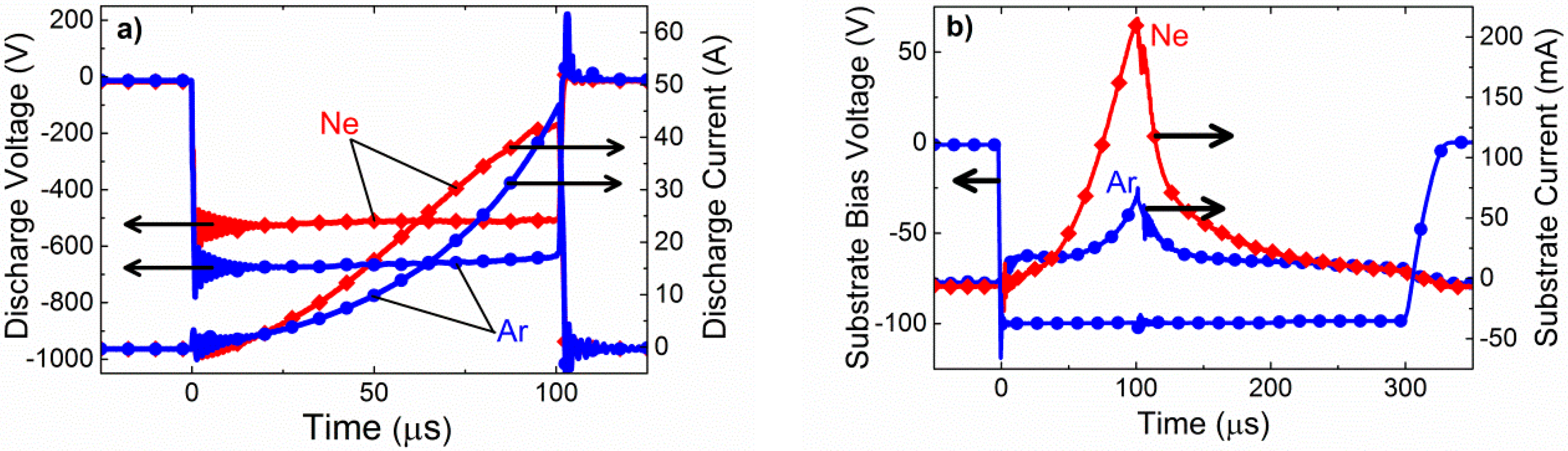
3.1. Process Characteristics

The discharge voltage and current waveforms, together with the substrate current from the Ar- and Ne-HiPIMS discharges are compared and presented in Figure 1. Despite the comparable discharge currents (Figure 1a), a considerably higher substrate current was obtained using Ne (Figure 1b), which means a higher amount of ions are reaching to the substrate in the Ne-HiPIMS process. The increased ionization in the Ne discharge, manifested by an increased substrate current, is due to an increased average electron energy (electron temperature) in the plasma discharge. A higher electron temperature in Ne is attributed to the higher ionization potential of Ne (21.56 eV) as compared to Ar (15.76 eV) since the electron temperature in a plasma discharge scales with the ionization potential of the process gas [19]. We measured the electron temperature and electron density for the two discharges and found out that the average energy of electrons (represented by Teff) in the Ne-HiPIMS discharge is indeed twice as high as in the Ar-HiPIMS discharge, Table 1.
The increase in the electron temperature yields a corresponding decrease in the mean ionization length of the sputtered C atoms [16], which entails a proportional increase in their ionized fraction. This was corroborated by the differences in ion-to-neutral ratios calculated from the substrate currents, Table 1. The total number of ions per deposited C atom was found to be three times higher for the Ne-HiPIMS case. A higher ion-to-neutral ratio shows that larger fluxes of C+ ions are generated in the Ne-HiPIMS discharge as compared to the Ar-HiPIMS, which are essential for tailoring film properties.

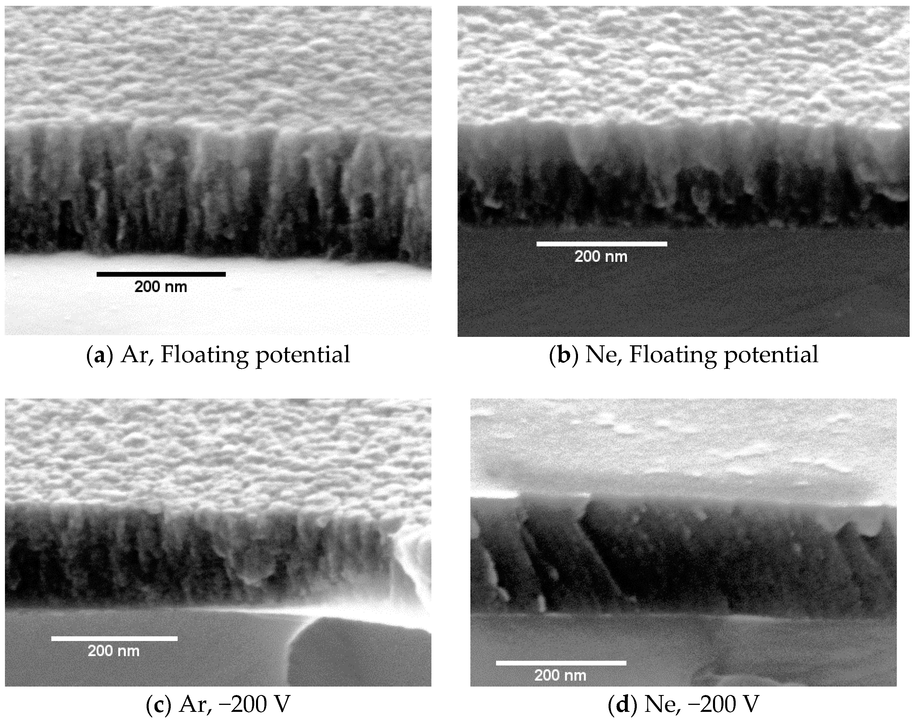
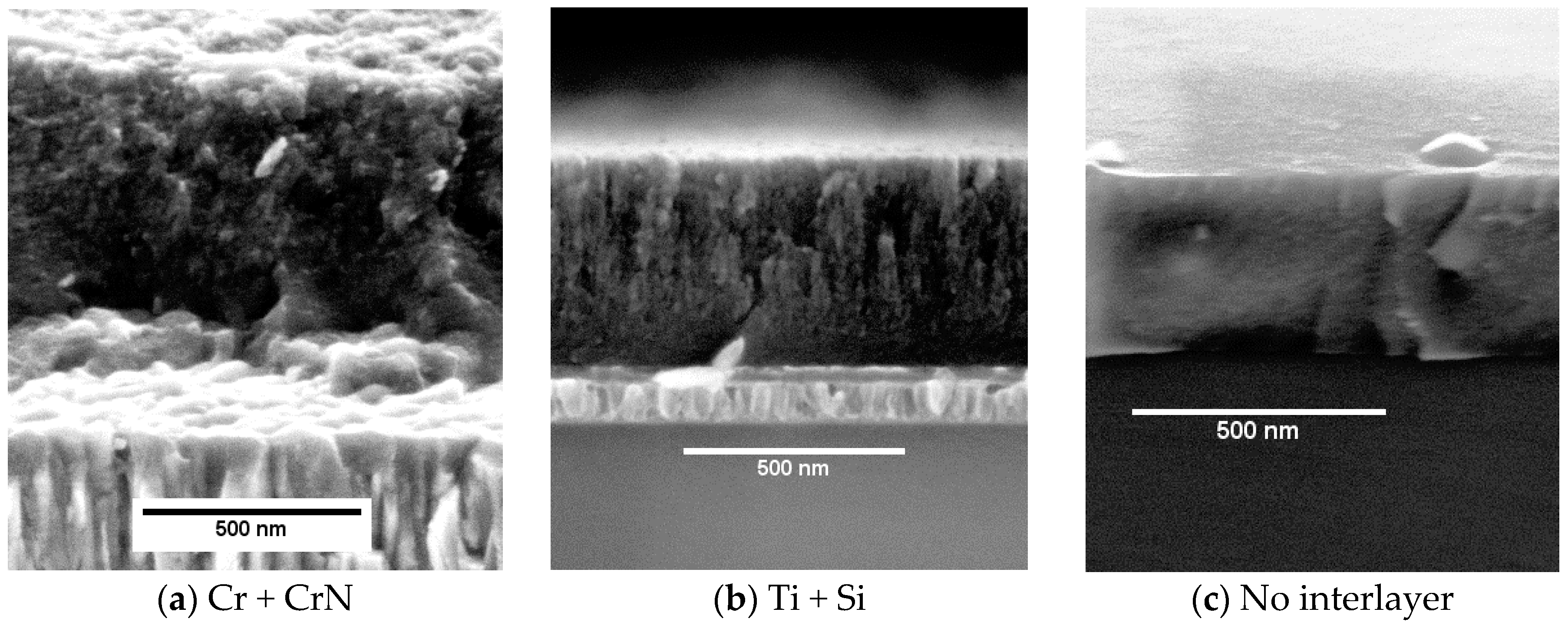
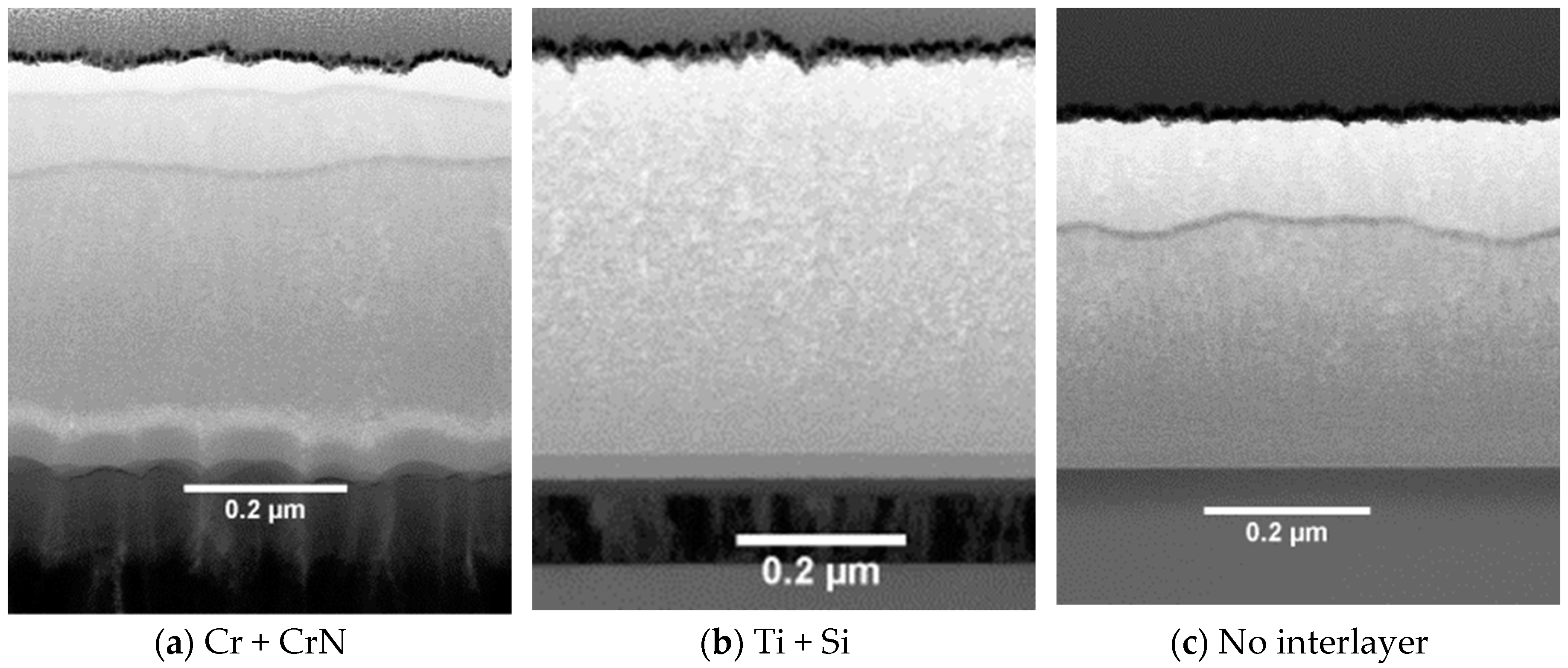
3.2. Structural Properties and Interfaces

The mass densities of the films grown using the Ar-HiPIMS process were found to be lower than those obtained using the Ne-HiPIMS process at all substrate bias voltage used [16]. The highest mass density of 2.7 g/cm3 was obtained using the Ne-HiPIMS process and the optimum substrate bias voltage of −200 V. The highest mass density obtained using the Ar-HiPIMS process at –200 V was ~2.5 g/cm3. The highest internal stress corresponding to the mass density of ~2.7 g/cm3 was ~2.5 GPa, which is about 2–3 times lower than those reported for similar mass densities for the films grown by a cathodic arc [4]. The Ne-HiPIMS films also exhibited better thermal stability as revealed by Raman spectroscopy of the annealed films. Typically, DLC films exhibit an increased disorder with an increase in annealing temperature [20]. The disorder is accompanied by a decrease in the sp3 bond fraction and the films exhibit a transition from a diamond-like to a graphite-like structure at a certain temperature [14]. Such a transition for the Ne-HiPIMS films, as manifested by an abrupt decrease in the full-width at half-maximum (FWHM) of the G-peak (FWHM-G) (Figure 2) occurred at ~400 °C and for the Ar-HiPIMS films at a lower temperature of ~200 °C. This demonstrated that the Ne-HiPIMS DLC films are thermally more stable than the Ar-HiPIMS DLC films. The Ne-HiPIMS film density decreased from about 2.65 g/cm3 to about 2.4 g/cm3 after annealing the film at 500 °C [15]. The overall higher values of the FWHM-G for the Ne-HiPIMS DLC films as compared to the Ar-HiPIMS DLC films imply a higher sp3 bond fraction [20], which is in agreement with their mass densities.
The beneficial effects of using Ne and the resulting large ionized flux of depositing carbon atoms were also observed in the microstructure of the grown films (Figure 3). The films were grown without any substrate bias voltage i.e., at the electrically floating potential (Figure 3a,b), as well as the Ar-HiPIMS DLC film deposited with −200 V bias (Figure 3c) exhibit similar columnar morphology features. The Ne-HiPIMS DLC film grown at the substrate bias voltage of −200 V (Figure 3d) exhibits a dramatic difference that is manifested by a smoother surface and denser microstructure. This shows that by generating large amounts of C+ ions and tuning their energy, dense and smooth DLC films can be grown. Overall, the microstructure of the films presented in Figure 3 is in line with the mass densities of the corresponding films.
The films with the microstructure presented in Figure 3 exhibited a good adhesion on Si at the nominal thickness of 500 nm. For deposition on steel, two different adhesion interlayers (Cr + CrN and Ti + Si) were evaluated. Cross-sectional images of the films deposited using these adhesion interlayers are shown in Figure 4 and Figure 5. The DLC deposited on the Ti + Si (Figure 4b) exhibits columnar microstructure. This is surprising given the smooth nature of the interlayer. In contrast, the DLC film on the Cr + CrN (Figure 4a) appears to be without columns.
TEM observations confirm the findings. The Cr + CrN interlayer (Figure 5a), despite being rough and columnar, leads to a non-columnar microstructure. Some defects in the DLC layer are initiated at the CrN columns and extend throughout the whole DLC thickness. The microstructure of the DLC film grown using the Ti + Si interlayer is very different, as shown in Figure 5b. The Ti + Si-DLC interface is very smooth. The DLC surface, however, is rough and the columns appear to open up more going towards the film surface. Figure 5c shows the TEM micrograph of the film grown on the Si substrate without any interlayer. The substrate-film interface is smooth and the film microstructure is non-columnar and dense, as it was also seen earlier in Figure 3d. The effect of the interlayers is counterintuitive and the mechanisms leading to the columnar growth on the Ti + Si interlayer is not clearly understood at present. The roughness evolution in amorphous materials is commonly attributed to the atomic shadowing [21]. A smooth interlayer such as the Ti + Si would be expected to lead to a smoother DLC microstructure than the rough Cr + CrN interlayer, which is in contrast to our findings.

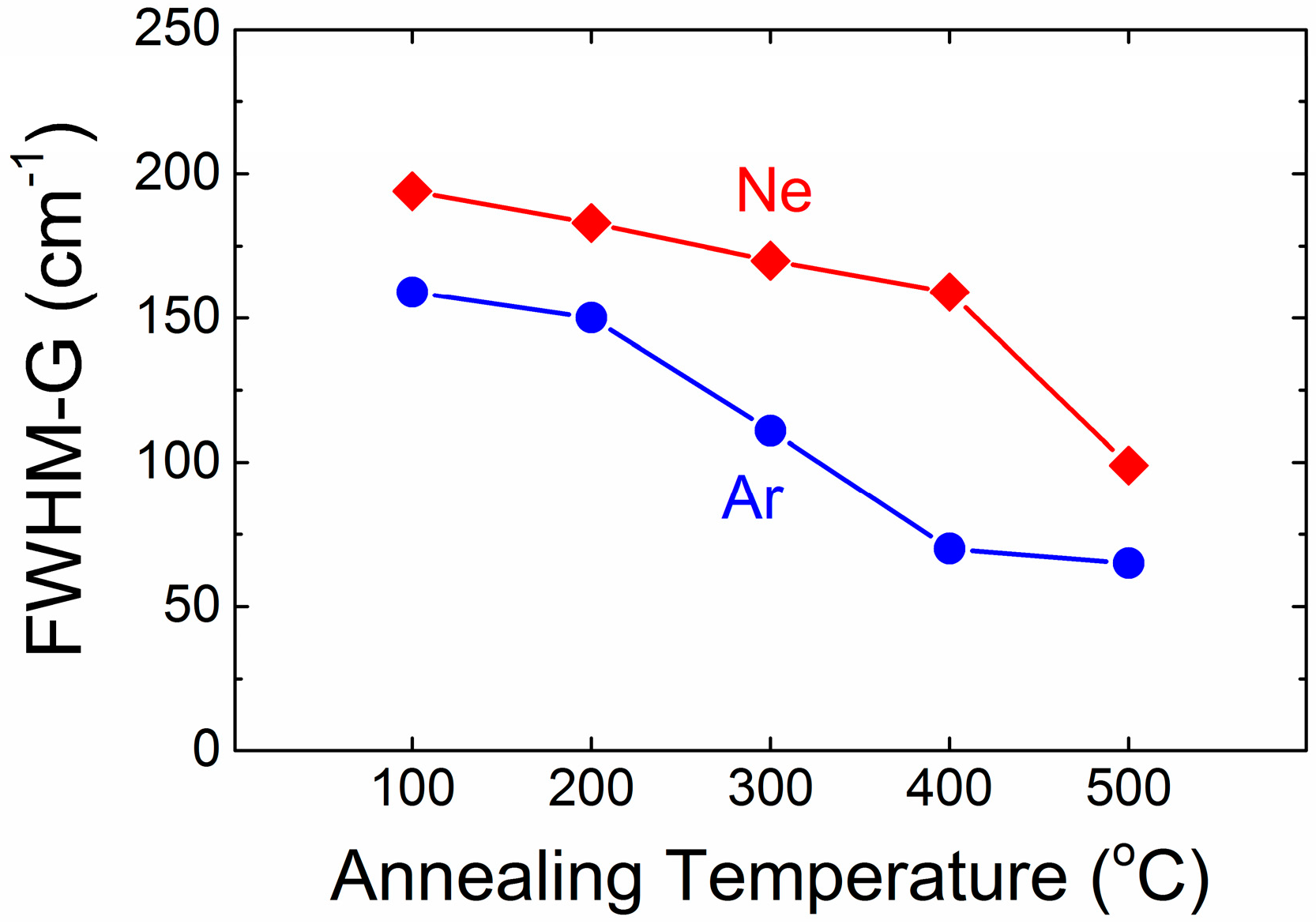
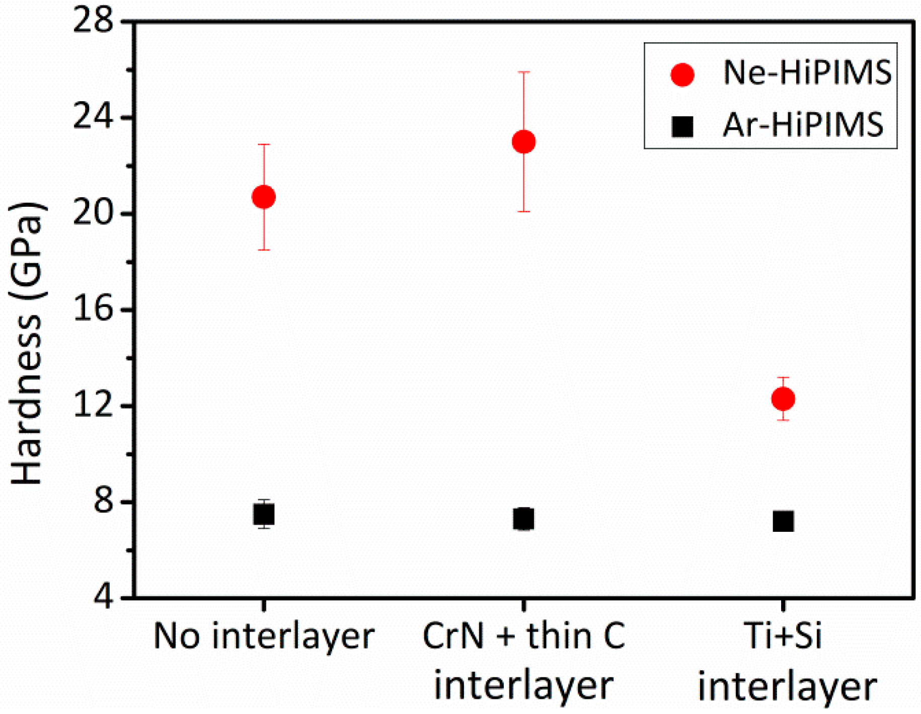
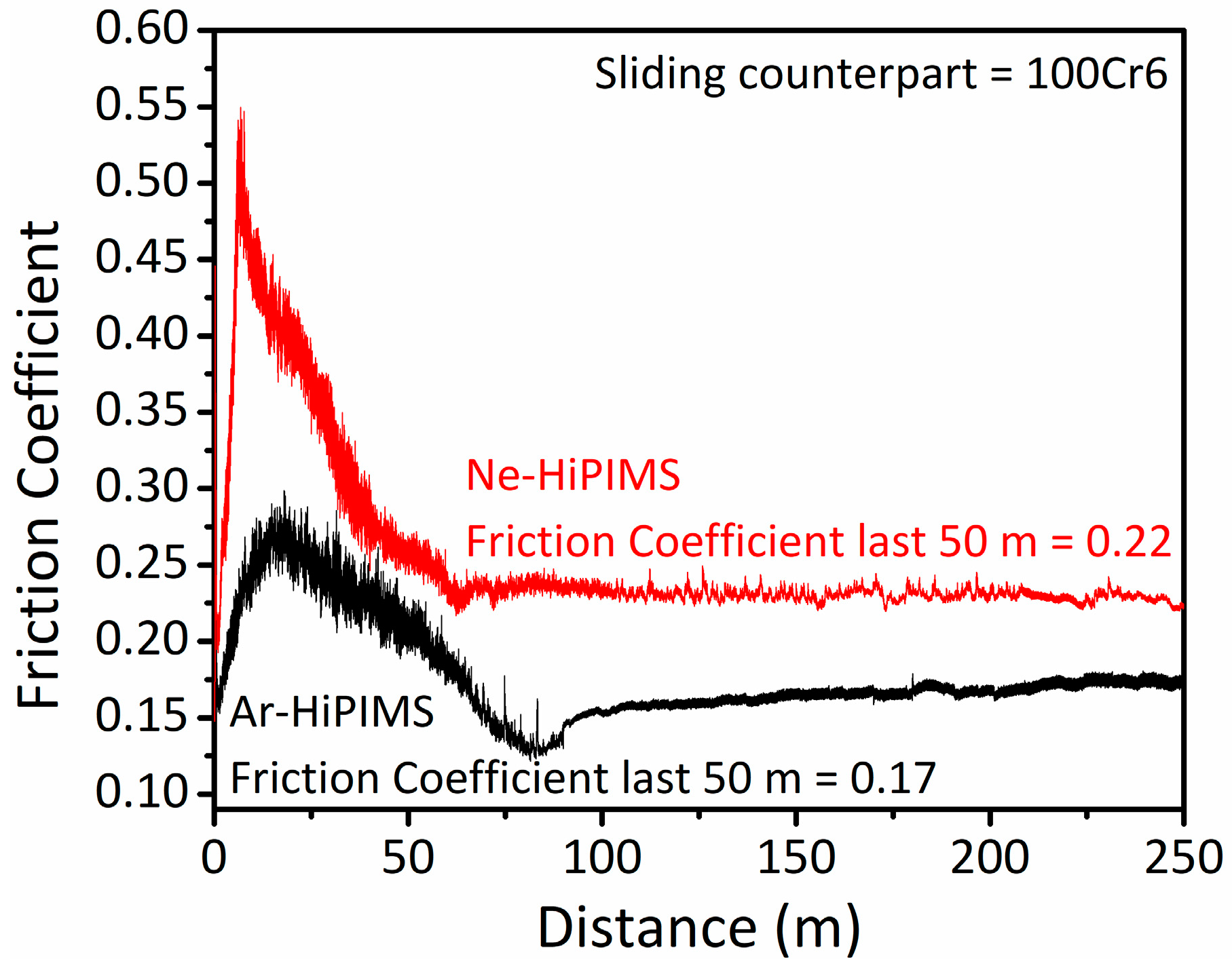
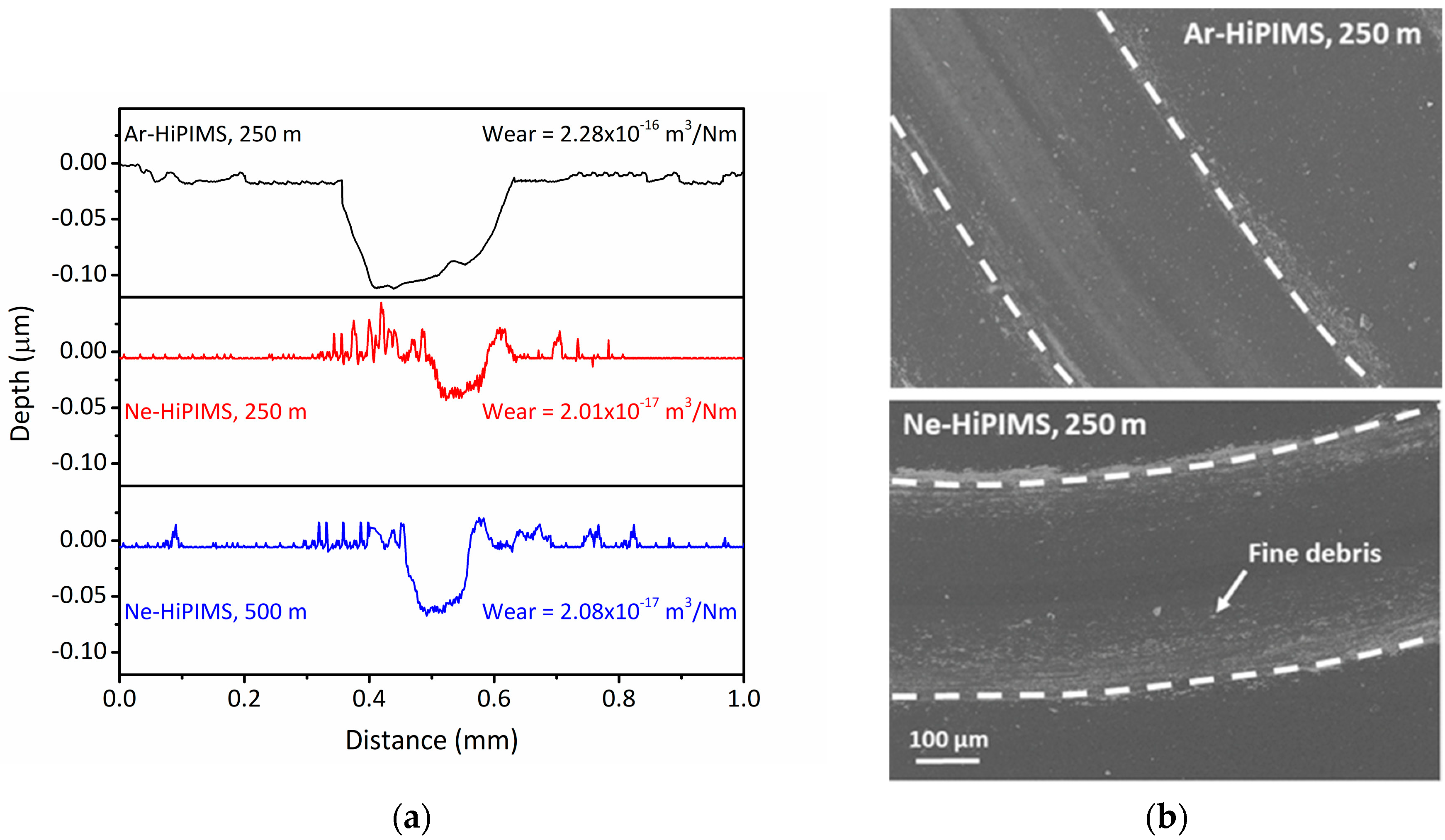
3.3. Mechanical Properties

The hardness of the Ar- and Ne-HiPIMS DLC films deposited at a substrate bias of −200 V onto different interlayers is presented in Figure 6. All DLC films deposited with Ar process gas exhibit a low hardness of ~7 GPa, regardless of the interlayer used. The hardness of the DLC films deposited with Ne process gas is above 20 GPa when the film was deposited directly on a Si substrate or onto the Cr + CrN interlayer. A much lower hardness, close to 12 GPa, was achieved for the film deposited onto the Ti + Si interlayer using the Ne-HiPIMS discharge. There is a strong correlation between the DLC hardness and the microstructure with the columnar films exhibiting a low hardness. In general, the mechanical properties of DLC films depend primarily on their mass density and sp3 fraction. Films with high density and high sp3 fraction exhibit a high hardness due to the strong and directional bonding between nearest neighbours, which results in the formation of a three-dimensional (tetrahedral) network of σ bonds [22]. Although the quantification of the sp3 fraction from Raman spectroscopy is difficult, the FWHM-G values (Figure 2) indicate an increased sp3 bond fraction. This is in agreement with the increased mass density as well as the higher transition temperature of the Ne-HiPIMS DLC films. The Ne-HiPIMS DLC film grown on the Ti + Si interlayer shows a lower hardness, which is in good agreement with the columnar morphology observed for this film.
Tribological tests were carried out on the DLC films deposited onto the Cr + CrN coated steel substrates, where the maximum hardness (23 GPa) was obtained for the Ne-HiPIMS deposited film. The corresponding Ar-HiPIMS DLC film was also characterized. Typical examples of the friction coefficient evolution during pin-on-disk tests are shown in Figure 7. The raw data was smoothed (10 points Savitzky–Golay smooth) to facilitate the analysis of the results. A running-in period with characteristic higher values of the friction coefficient is observed at the beginning of both tests. During the running-in period, the Ne-HiPIMS DLC film reached higher values of friction coefficient (0.53) compared to those achieved by the Ar-HiPIMS DLC film (0.27). Both films reached a steady-state regime within the first 100 m of the tests, as indicated by the stable value of friction coefficient at higher distances. The average value of the friction coefficient over the last 50 m of sliding, i.e., within the steady-state regime, is also indicated in the figure. The values, 0.22 and 0.17 for the Ne-HiPIMS and Ar-HiPIMS DLC, respectively, are comparable to the values typical for carbon-based films tested at ambient conditions [23].
In spite of the somewhat higher friction coefficient of the Ne-HiPIMS DLC film, the wear rate was about an order of magnitude lower than that of the corresponding Ar-HiPIMS DLC. Two-dimensional profiles of the wear tracks obtained at the end of the pin-on-disk tests (depicted in Figure 8a) clearly show that, after 250 m of sliding, the depth and width of the wear tracks are much larger for the Ar-HiPIMS DLC than for the Ne-HiPIMS DLC film. Increasing the total sliding distance to 500 m resulted in a similar wear rate for the Ne-HiPIMS DLC film similar to that measured at a shorter sliding distance. The wear rate of the films agrees well with the expected inverse proportional relation between this property and the hardness of the films [24].
As shown by Voevodin et al., the friction of the DLC films is controlled by the formation of a graphitic transfer layer during the wear process of the sliding couple, which has a lubricating effect and reduces the friction coefficient [25,26]. As exemplified by the SEM micrographs in Figure 8b, fine wear debris particles are dispersed over the surface of the wear tracks of both films. However, a significantly higher amount of debris is found over the wear track of the Ne-HiPIMS DLC film and the particles are concentrated near the edge of the race track, as indicated by the corresponding 2D profiles. These results suggest that the wear of the Ne-HiPIMS DLC film proceeds by successive formation of fine particles which agglomerate at the outer parts of the wear track and, thus, a higher friction coefficient was found for this film. In contrast, the wear of the Ar-HiPIMS DLC film involves a layer-by-layer removal of the film, which is characteristic of sp2-rich films, and thus explains its lower friction coefficient.
Typically, the wear rate of ta-C films in humid environments varies from 10−16 to 10−18 m3/Nm while their friction coefficient is within the range of 0.1–0.2 [23]. The wear rate of the Ne-HiPIMS DLC film deposited in this work falls within the range of typical ta-C values. In this study, however, magnetron sputtering was used in contrast to the cathodic arc or pulsed laser deposition commonly employed for ta-C. Magnetron sputtering is an attractive deposition technique and the use of Ne is, therefore, an interesting option for tribological coatings. Although the hardness of the film is lower than that of the state-of-the-art ta-C films deposited by filtered cathodic arc or pulsed laser deposition, the tribological properties are already very interesting for many applications. Given the improved thermal stability of the Ne-HiPIMS films up to temperatures close to 500 °C [15], the Ne-HiPIMS DLC is a possible candidate to replace CrN for coatings of piston rings for internal combustion engines. At present, CrN films are used due to their excellent oxidation resistance, thermal stability, and high hardness [27]. However, the high friction coefficient of CrN, typically close to 0.75 against steel, results in much higher wear rates of the CrN films (≈1.1 × 10⁻¹⁶ m3/Nm) in spite of similar hardness values [28].

4. Conclusions

In summary, we have demonstrated that the Ne-HiPIMS process leads to DLC films with significantly improved structural and mechanical properties, compared to the corresponding Ar-HiPIMS process. The improved properties of the Ne-HiPIMS DLC films were attributed to an enhanced C ionization in the Ne discharge. The Ne-HiPIMS DLC films exhibit a dense microstructure without columns and an increased mass density (up to 2.65 g/cm3). The hardness of the Ne-HiPIMS films reached up to 23 GPa when deposited on steel with a Cr + CrN adhesion interlayer, much higher than the 8 GPa observed for Ar-HiPIMS. The higher hardness of the DLC films deposited with the Ne-HiPIMS discharge is in line with their higher mass density. Raman spectroscopy indicates an increased sp3 fraction in the Ne-HiPIMS DLC films, although the values were not quantified. Tribological testing by pin-on-disk revealed a friction coefficient of 0.22 against steel and a wear rate of 2 × 10⁻¹⁷ m3/Nm, which is about an order of magnitude lower than that of the films deposited in pure Ar. Despite the film hardness being lower than that of the state-of-the-art ta-C films deposited by cathodic arc, the low wear rate makes the material very interesting for many applications.

Author Contributions

A.A. carried out synthesis and structural characterization of the DLC films and wrote major part of the manuscript. F.F. performed tribological tests and evaluated the results. J.C.O supervised interlayer development and mechanical characterization, and wrote parts of the manuscript. T.K. conceived the project, designed structure of the article, and revised the article.

Funding

The work was supported by M-ERA.Net project TANDEM through Vinnova and FCT–Fundação para a Ciência e a Tecnologia (M-ERANET/0003/2015).

Acknowledgments

Lars Riekehr from Uppsala University is gratefully acknowledged for TEM characterization.

Conflicts of Interest

The authors declare no conflict of interest.

References

  1. Erdemir, A.; Donnet, C. Tribology of diamond-like carbon films: Recent progress and future prospects. J. Phys. D Appl. Phys. 2006, 39, R311. [Google Scholar] [CrossRef]
  2. Sui, X.; Liu, J.; Zhang, S.; Yang, J.; Hao, J. Microstructure, mechanical and tribological characterization of CrN/DLC/Cr-DLC multilayer coating with improved adhesive wear resistance. Appl. Surf. Sci. 2018, 439, 24–32. [Google Scholar] [CrossRef]
  3. Duminica, F.D.; Belchi, R.; Libralesso, L.; Mercier, D. Investigation of Cr(N)/DLC multilayer coatings elaborated by PVD for high wear resistance and low friction applications. Surf. Coat. Technol. 2018, 337, 396–403. [Google Scholar] [CrossRef]
  4. Chhowalla, M. Thick, well-adhered, highly stressed tetrahedral amorphous carbon. Diam. Relat. Mater. 2001, 10, 1011–1016. [Google Scholar] [CrossRef]
  5. Polo, M.C.; Andújar, J.L.; Hart, A.; Robertson, J.; Milne, W.I. Preparation of tetrahedral amorphous carbon films by filtered cathodic vacuum arc deposition. Diam. Relat. Mater. 2000, 9, 663–667. [Google Scholar] [CrossRef]
  6. Voevodin, A.A.; Donley, M.S.; Zabinski, J.S. Pulsed laser deposition of diamond-like carbon wear protective coatings: A review. Surf. Coat. Technol. 1997, 92, 42–49. [Google Scholar] [CrossRef]
  7. Sheeja, D.; Tay, B.K.; Leong, K.W.; Lee, C.H. Effect of film thickness on the stress and adhesion of diamond-like carbon coatings. Diam. Relat. Mater. 2002, 11, 1643–1647. [Google Scholar] [CrossRef]
  8. Ferrari, A.C.; Libassi, A.; Tanner, B.K.; Stolojan, V.; Yuan, J.; Brown, L.M.; Rodil, S.E.; Kleinsorge, B.; Robertson, J. Density, sp3 fraction, and cross-sectional structure of amorphous carbon films determined by X-ray reflectivity and electron energy-loss spectroscopy. Phys. Rev. B 2000, 62, 11089. [Google Scholar] [CrossRef]
  9. Grill, A. Diamond-like carbon: State of the art. Diam. Relat. Mater. 1999, 8, 428–434. [Google Scholar] [CrossRef]
  10. Neuville, S. Antiwear material criteria. JPJ Solids Struct. 2009, 3, 33–42. [Google Scholar]
  11. Robertson, J. Diamond-like amorphous carbon. Mater. Sci. Eng. R 2002, 37, 129–281. [Google Scholar] [CrossRef] [Green Version]
  12. Davis, C.A. A simple model for the formation of compressive stress in thin films by ion bombardment. Thin Solid Films 1993, 226, 30–34. [Google Scholar] [CrossRef]
  13. Marks, N.A.; McKenzie, D.R.; Pailthorpe, B.A. Molecular-dynamics study of compressive stress generation. Phys. Rev. B 1996, 53, 4117. [Google Scholar] [CrossRef]
  14. Ferrari, A.C.; Kleinsorge, B.; Morrison, N.A.; Hart, A.; Stolojan, V.; Robertson, J. Stress reduction and bond stability during thermal annealing of tetrahedral amorphous carbon. J. Appl. Phys. 1999, 85, 7191–7197. [Google Scholar] [CrossRef]
  15. Aijaz, A.; Kubart, T. Ion induced stress relaxation in dense sputter-deposited DLC thin films. Appl. Phys. Lett. 2017, 111, 051902. [Google Scholar] [CrossRef]
  16. Aijaz, A.; Sarakinos, K.; Lundin, D.; Brenning, N.; Helmersson, U. A strategy for increased carbon ionization in magnetron sputtering discharges. Diam. Relat. Mater. 2012, 23, 1–4. [Google Scholar] [CrossRef] [Green Version]
  17. Aijaz, A.; Louring, S.; Lundin, D.; Kubart, T.; Jensen, J.; Sarakinos, K.; Helmersson, U. Synthesis of hydrogenated diamondlike carbon thin films using neon-acetylene based high power impulse magnetron sputtering discharges. J. Vac. Sci. Technol. A 2016, 34, 061504. [Google Scholar] [CrossRef]
  18. Janssen, G.C.A.M.; Abdalla, M.M.; van Keulen, F.; Pujada, B.R.; van Venrooy, B. Celebrating the 100th anniversary of the stoney equation for film stress: Developments from polycrystalline steel strips to single crystal silicon wafers. Thin Solid Films 2009, 517, 1858–1867. [Google Scholar] [CrossRef]
  19. Hopwood, J.A. Plasma physics. In Thin Films: Ionized Physical Vapor Deposition; Academic Press: San Diego, CA, USA, 2000; Volume 27, pp. 181–207. [Google Scholar]
  20. Ferrari, A.C.; Robertson, J. Interpretation of Raman spectra of disordered and amorphous carbon. Phys. Rev. B 2000, 61, 14095. [Google Scholar] [CrossRef]
  21. Lifshitz, Y.; Edrei, R.; Hoffman, A.; Grossman, E.; Lempert, G.D.; Berthold, J.; Schultrich, B.; Jager, H.U. Surface roughness evolution and growth mechanism of carbon films from hyperthermal species. Diam. Relat. Mater. 2007, 16, 1771–1776. [Google Scholar] [CrossRef]
  22. Lifshitz, Y. Diamond-like carbon—Present status. Diam. Relat. Mater. 1999, 8, 1659–1676. [Google Scholar] [CrossRef]
  23. Donnet, C.; Erdemir, A. Tribology of Diamond-Like Carbon Films: Fundamentals and Applications; Springer: New York, NY, USA, 2008. [Google Scholar]
  24. Martınez, E.; Andújar, J.L.; Polo, M.C.; Esteve, J.; Robertson, J.; Milne, W.I. Study of the mechanical properties of tetrahedral amorphous carbon films by nanoindentation and nanowear measurements. Diam. Relat. Mater. 2001, 10, 145–152. [Google Scholar] [CrossRef]
  25. Voevodin, A.A.; Phelps, A.W.; Zabinski, J.S.; Donley, M.S. Friction induced phase transformation of pulsed laser deposited diamond-like carbon. Diam. Relat. Mater. 1996, 5, 1264–1269. [Google Scholar] [CrossRef]
  26. Ming, M.Y.; Piliptsou, D.G.; Rudenkov, A.S.; Rogachev, A.V.; Jiang, X.H.; Sun, D.P.; Chaus, A.S.; Balmakou, A. Structure, mechanical and tribological properties of Ti-doped amorphous carbon films simultaneously deposited by magnetron sputtering and pulse cathodic arc. Diam. Relat. Mater. 2017, 77, 1–9. [Google Scholar] [CrossRef]
  27. Chen, L.; Paulitsch, J.; Du, Y.; Mayrhofer, P.H. Thermal stability and oxidation resistance of Ti–Al–N coatings. Surf. Coat. Technol. 2012, 206, 2954–2960. [Google Scholar] [CrossRef] [PubMed]
  28. Lin, J.; Sproul, W.D.; Moore, J.J. Tribological behavior of thick CrN coatings deposited by modulated pulsed power magnetron sputtering. Surf. Coat. Technol. 2012, 206, 2474–2483. [Google Scholar] [CrossRef]
Figure 1. (a) The discharge voltage and current waveforms of a Ne- and Ar-HiPIMS discharge and (b) substrate bias voltage and current measured for the Ne- and Ar-HiPIMS discharges.
Coatings 08 00385 g001
Figure 2. The full-width at half-maximum of the G-peak measured after annealing the Ne- and Ar-HiPIMS films deposited with a bias voltage of −200 V.
Coatings 08 00385 g002
Figure 3. The cross-sectional SEM images of 180-nm thick Ar-HiPIMS and Ne-HiPIMS DLC films deposited on Si at the electrically floating potential and −200 V substrate bias. All samples were 20° tilted to show both the surface and the cleaved cross-section.
Coatings 08 00385 g003
Figure 4. The cross-sectional SEM images of the Ne-HiPIMS DLC film deposited at −200 V of substrate bias on (a) Cr + CrN, (b) Ti + Si interlayers and (c) directly on a Si substrate for a reference.
Coatings 08 00385 g004
Figure 5. The cross-sectional TEM images of the Ne-HiPIMS DLC film deposited at −200 V of substrate bias on (a) Cr + CrN, and (b) Ti + Si interlayers, as well as on (c) a Si substrate without any interlayer. The horizontal lines in (a) and (c) are artifacts of the FIB sample preparation.
Coatings 08 00385 g005
Figure 6. The hardness of the Ar- and Ne-HiPIMS DLC films deposited at the substrate bias of −200 V on a Si substrate as well as on the Ti + Si and Cr + CrN interlayers.
Coatings 08 00385 g006
Figure 7. The friction coefficient of the DLC coatings deposited by the Ar and Ne-HiPIMS processes.
Coatings 08 00385 g007
Figure 8. (a) The 2D profiles of the wear track of coatings tested against 100Cr6 balls and (b) SEM images of wear tracks. An additional test for 500 m was performed on the Ne-HiPIMS DLC film.
Coatings 08 00385 g008
Table 1. The plasma parameters, electron temperature Teff and plasma density ne, together with an ion-to-neutral ratio of the Ar- and Ne-HiPIMS discharges.
ProcessTeff (eV)ne (m−3)Ion-to-Neutral Ratio
Ar-HiPIMS11 × 10170.4
Ne-HiPIMS25 × 10161.3

