Article

Sputter-Deposited Indium–Tin Oxide Thin Films for Acetaldehyde Gas Sensing

Department of Engineering Sciences, The Ångström Laboratory, Uppsala University, P.O. Box 534, SE-751 21 Uppsala, Sweden
*
Author to whom correspondence should be addressed.
Coatings 2016, 6(2), 19; https://doi.org/10.3390/coatings6020019
Submission received: 24 March 2016 / Revised: 8 April 2016 / Accepted: 11 April 2016 / Published: 14 April 2016

Abstract

:
Reactive dual-target DC magnetron sputtering was used to prepare In–Sn oxide thin films with a wide range of compositions. The films were subjected to annealing post-treatment at 400 °C or 500 °C for different periods of time. Compositional and structural characterizations were performed by X-ray photoelectron spectroscopy, energy dispersive X-ray spectroscopy, X-ray diffraction, Rutherford backscattering and scanning electron microscopy. Films were investigated for gas sensing at 200 °C by measuring their resistance response upon exposure to acetaldehyde mixed with synthetic air. We found that the relative indium-to-tin content was very important and that measurable sensor responses could be recorded at acetaldehyde concentrations down to 200 ppb, with small resistance drift between repeated exposures, for both crystalline SnO2-like films and for amorphous films consisting of about equal amounts of In and Sn. We also demonstrated that it is not possible to prepare crystalline sensors with intermediate indium-to-tin compositions by sputter deposition and post-annealing up to 500 °C.

Graphical Abstract

1. Introduction

Monitoring of indoor air quality is of great importance since people in industrialized countries spend as much as 80% to 90% of their time inside buildings or vehicles [1]. Poor indoor air quality has been associated with the so-called “sick building syndrome”, which refers to situations in which the users of the building develop diffuse disease symptoms and discomfort connected with the time spent in some buildings without acquiring any specific illness [2]. One of the major causes of the sick building syndrome is volatile organic compounds (VOCs) released from interior surfaces and outdoor sources entering and accumulating in buildings. Other reasons include inadequate ventilation and biological contaminants such as bacteria and viruses. Monitoring the level of VOCs clearly is a key issue for assessing indoor air quality.
Among the VOCs, acetaldehyde is important since it is highly reactive and irritating to the skin, eyes and respiratory tract. It is also highly odorous; the human perception limit in air is as low as 70 ppb [3]. Potential sources for acetaldehyde emissions include various combustion processes (wood, wastes, fossil fuels, tobacco, etc.) [4], and acetaldehyde can also be emitted by, e.g., polymeric building materials and emulsion paints, and it can be an intermediate in the natural respiration of plants [5,6]. The threshold limit value for adverse health effects is 25 ppm, and the maximum permissible workplace concentration is 50 ppm [3]. Acetaldehyde concentrations exceeding 50 ppm are extremely irritating and possibly carcinogenic [5].
Semiconducting metal oxides (SMOXs) are attractive for uses in gas sensing applications as a consequence of their low cost, production flexibility and simplicity of use [7]. The sensing relies on resistance changes of thin films as a result of surface-chemical reactions [8,9,10,11]. SMOX sensors have been used to monitor acetaldehyde [12] and other VOCs such as formaldehyde [13,14,15,16] for almost 50 years [17]. Various fabrication methods, including sputter deposition and evaporation, have been used to manufacture SMOX gas sensors [18,19].
Among several SMOX sensors, nanocrystalline In4Sn3O12 oxide produced by high temperature flame spray pyrolysis has recently been suggested as a promising sensor material [20]. The object of the present work is to elaborate on this latter study, and investigate In–Sn oxide thin film sensors with a wide range of compositions produced by sputter deposition, which is a versatile deposition technique amenable to industrial upscaling. We compare acetaldehyde sensing by as-deposited and annealed sputter-deposited films of various compositions and explore the possible composition and post-annealing conditions consistent with this approach. We show that the relative In and Sn content is important, and that measureable sensor responses to acetaldehyde can be detected at concentrations as low as 200 ppb at 200 °C with amorphous In–Sn oxide sensors as well as with crystalline SnO2-like sensors. Moreover, we show that it is not possible to prepare crystalline sensors with intermediate In:Sn composition by sputtering and post-annealing up to 500 °C.

2. Materials and Methods

2.1. Film Preparation

Indium–tin oxide thin films were deposited onto unheated glass substrates by reactive DC magnetron co-sputtering from two targets using a versatile deposition system with a base pressure of 2 × 10⁻⁵ Pa. Two 5-cm-diameter targets consisting of 99.99% pure In(3 wt.%)–Sn(97 wt.%) and In(90 wt.%)–Sn(10 wt.%) were positioned 13 cm from the substrates; these target compositions are commercially available. Depositions were performed for 15 min and the substrate holder was rotated to ensure even films. Ar and O2 gas flow rates—fAr and fO2, respectively—were adjusted by mass flow controllers in order to get a constant pressure p in the sputter plasma. Sputtering conditions for a series of samples, denoted A–F, are presented in Table 1.
Three sets of samples were prepared and subjected to different annealing post-treatments: (i) as-deposited films, (ii) films annealed at 400 °C in air for 30 min, and (iii) films annealed at 400 °C in air for 6 h. In case (ii), the temperature was ramped up from 25 °C to 400 °C at ~11 °C/min and was ramped back to 25 °C at ~2.8 °C/min; in case (iii), the temperature was ramped up from 25 °C to 400 °C at ~4.7 °C/min and was ramped back to 25 °C at ~1.8 °C/min. Furthermore, samples C, D and E were subjected to an additional annealing step at 500 °C in air for 12 h. The temperature was ramped up from 25 °C to 500 °C at ~4.2 °C/min and then ramped down to 25 °C at a rate of ~1.8 °C/min.

2.2. Film Characterization: Techniques

The relative amounts of In and Sn atoms were determined by X-ray photoelectron spectroscopy (XPS) using a PHI Quantum 2000 instrument with AlKα1 radiation at 1486.6 eV and an electron flood gun was used for charge compensation. In and Sn contents were calculated with the Multipak software v6.1A (Physical Electronics, Inc., Chanhassen, MN, USA). In order to record the In 3d5 and Sn 3d5 peaks, the pass energy was set to 29.35 eV, the scan resolution was 0.25 eV, and the neutralizer voltage was 1.0 V. The XPS peak at 284.8 eV, due to adventitious carbon, was used to calibrate the energy scale. The amounts of In and Sn in the films were also confirmed by energy-dispersive X-ray spectroscopy (EDS), using an 80 mm2 Silicon Drift Detector in a Zeiss Leo 1550 scanning electron microscope (SEM) with the AZtec software for element analysis. The concentrations of In and Sn (in percentage), determined by EDS and XPS, are reported relative to the sum of In and Sn. The oxygen concentration was estimated from Rutherford backscattering spectroscopy (RBS) performed at the Tandem Laboratory of Uppsala University and using He2+ ions with energy of 2 MeV. RBS data were analyzed using the SIMNRA program [21].
Grazing incidence angle X-ray diffraction (XRD) data were acquired using a Siemens 5000 diffractometer (Siemens/Bruker, Karlsruhe, Germany) with CuKα1 radiation, with a 2θ range from 20° to 90°. Film morphology was determined by SEM, using a Zeiss LEO 1550 FEG instrument with in-lens detector (Carl Zeiss NTS GmbH, Oberkochen, Germany). The film thicknesses were measured to be 150 ± 40 nm as recorded by a Veeco Dektak 150 surface profilometry instrument (Bruker, Tucson, AZ, USA).

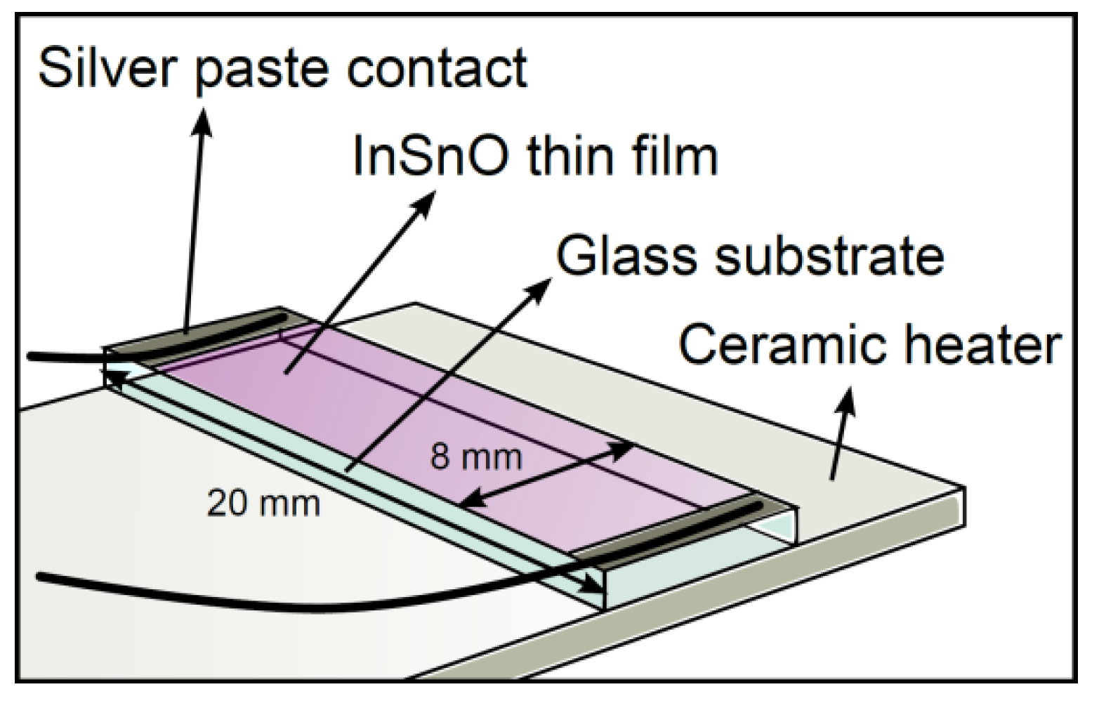
2.3. Gas Sensing Setup

Gas sensing measurements were performed in a 300 mL stainless steel chamber connected to a gas handling system via mass flow controllers. Sensor resistances were recorded at acetaldehyde concentrations between 0.2 and 25 ppm. The sensors were biased with 5 V and two-point-probe resistance was extracted from the measured electric current through the sensors. Gas sensing measurements were carried out at 200 °C. No significant responses were observed at lower operation temperatures. At the beginning of each measurement the sensors were stabilized at 200 °C in 200 mL/min flow of synthetic air (80% N2 and 20% O2) for 4 h. Three cycles of intermittent synthetic air (30 min) and acetaldehyde (30 min) gas exposure were then performed in a gas flow of 200 mL/min, and dry synthetic air was admitted in the last 1-h-cycle to monitor the resistance drift per exposure cycle for the sensor. The sensor setup is schematically depicted in Figure 1.

3. Results and Discussion

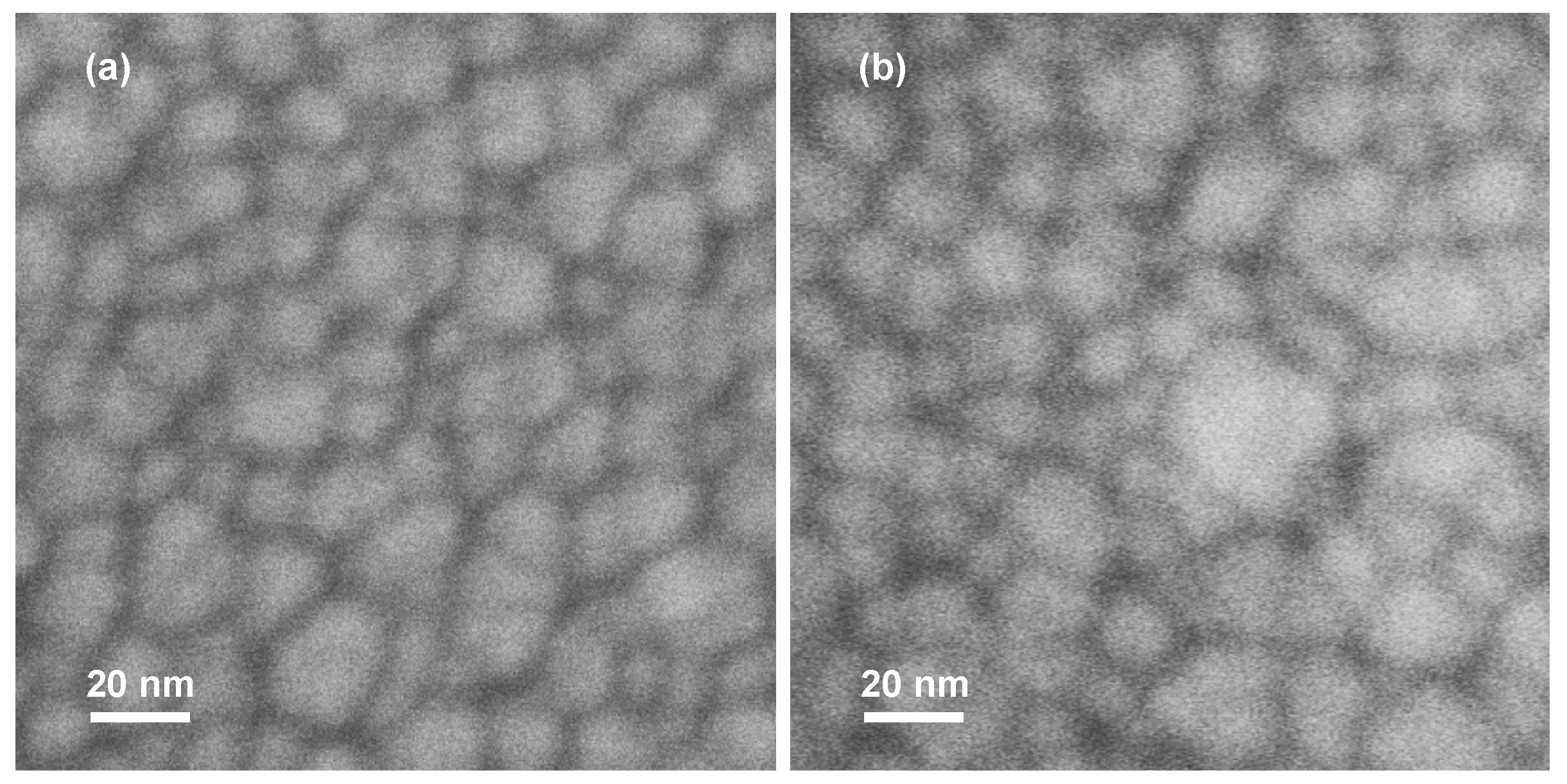
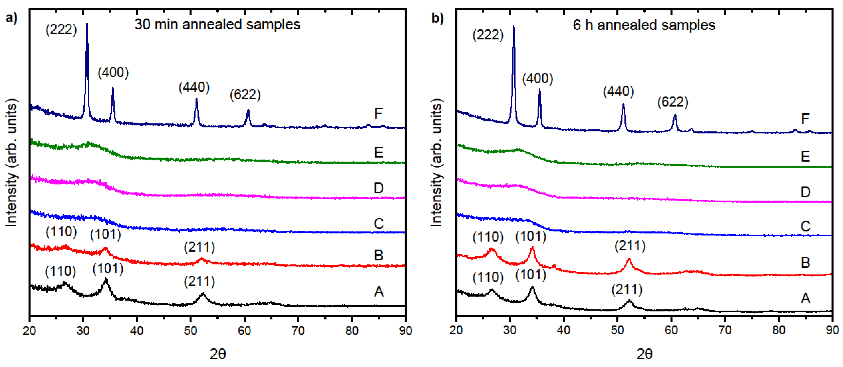
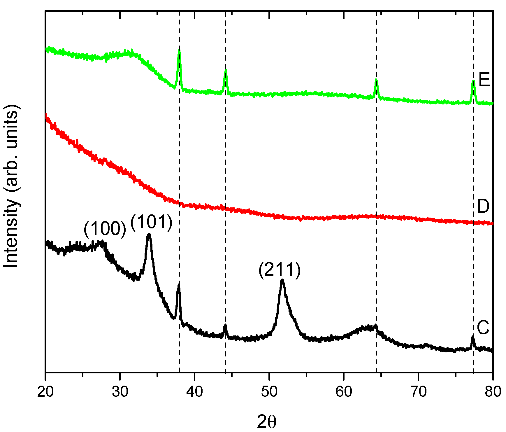
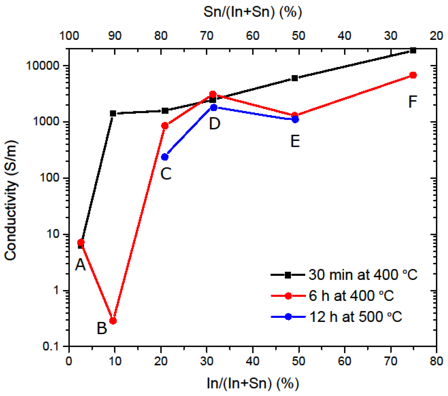
3.1. Film Characterization: Data

Table 2 shows the thickness and chemical composition of films after deposition (as-deposited) and after annealing at 400 °C for 6 h. Due to inherent uncertainties in quantifying oxygen in the nanostructured In–Sn oxide films with XPS or EDS, oxygen-to-metal ratios were measured with RBS. In and Sn peaks overlap in RBS data as a result of similar atomic masses, and XPS and EDS were therefore used to extract the In and Sn concentrations. Table 2 shows that the Sn and In concentrations of the films varied from about 3% In + 97% Sn for sample A, using only sputter target 1, to about 75% In + 25% Sn for sample F, using only sputter target 2. It is evident from the latter data that some preferential Sn sputtering occurs. The results for XPS and EDS do not show significant differences.
SEM images show that all films exhibit a nanostructured morphology consisting of aggregates with dimensions between 10 and 20 nm. The nanostructure was essentially the same in the as-deposited samples and after its annealing post-treatment. Typical film morphologies are shown in Figure 2. A few larger aggregates, 50–100 nm in size, were occasionally observed in the films; they had the same In and Sn content as the rest of the films, as demonstrated by EDS.
XRD analysis of samples annealed for 30 min and 6 h at 400 °C revealed different film structures depending on their In and Sn contents. As shown in Figure 3, when the In/(Sn + In) ratio is below 20% the films have a tendency to form a tetragonal SnO2 structure corresponding to the reference pattern ICDD:00-021-1250 (International Centre for Diffraction Data). Furthermore, it is observed that the crystallite size varied depending on the composition. By applying the Scherrer equation [22] to the <101> reflection peak at 33.89°, the crystallite sizes for sample A were calculated to be ~4.8 nm and ~6.0 nm after annealing for 30 min and 6 h, respectively. The corresponding crystallite sizes for sample B were ~4.3 nm and ~6.1 nm. Samples C, D and E were found to be amorphous according to XRD, irrespective of annealing time up to 400 °C. Film F exhibited a crystal structure that can be assigned to cubic In2O3 in agreement with the reference pattern ICDD:00-006-0416. By applying the Scherrer equation to the <222> peak at 30.58° for sample F, crystallite sizes of ~18.1 nm and ~18.4 nm were calculated for those films annealed for 30 min and 6 h up to 400 °C, respectively, i.e., the cubic In2O3 crystallites were much larger than for the SnO2 structure. It is apparent that the crystallite sizes do not agree with the features observed in SEM images and that the nanostructures seen in SEM consist of aggregated crystals.
After annealing at 500 °C for 12 h, samples C, D and E revealed different results depending on their In/(In + Sn) ratios (Figure 4). Sample C, with a measured In/(In + Sn) ratio of 21%, showed a tetragonal SnO2 structure and a crystallite size of 6.4 nm as calculated from the Scherrer equation using the <101> peak. In contrast, samples D and E remained amorphous after annealing at 500 °C, which is consistent with results in a previous study by Isomäki et al. [23].
Electrical conductivity was calculated from resistance recordings at 200 °C prior to the gas sensing measurements for samples annealed at different temperatures and periods of time. As seen in Figure 5, the conductivity is almost the same, irrespective of annealing time, for the most Sn-rich sample A. When the In content is increased, there is a sharp increase in conductance, which occurs at a smaller In content in samples annealed for 30 min than in samples annealed for 6 h. The transition appears to depend critically on the In composition and the associated film structure, which may explain the dramatic variations of the conductance at low In concentrations for different annealing temperatures (30 min and 6 h, respectively, in Figure 5). For In/(In + Sn) contents exceeding 10%, there is, however, a consistent overall increasing trend of the conductance with increasing amounts of In, while longer annealing times tend to yield lower conductivity. For samples C, D and E, subjected to a higher annealing temperature of 500 °C for 12 h, a slight decrease in conductivity was observed.

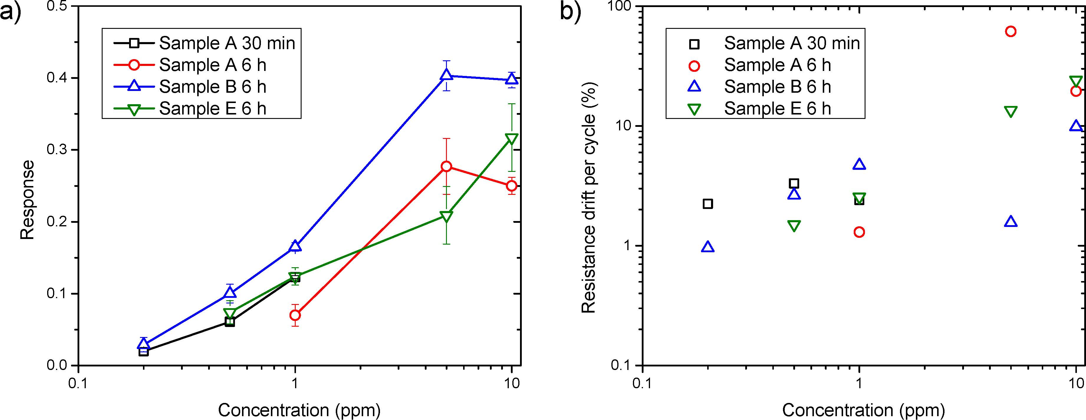
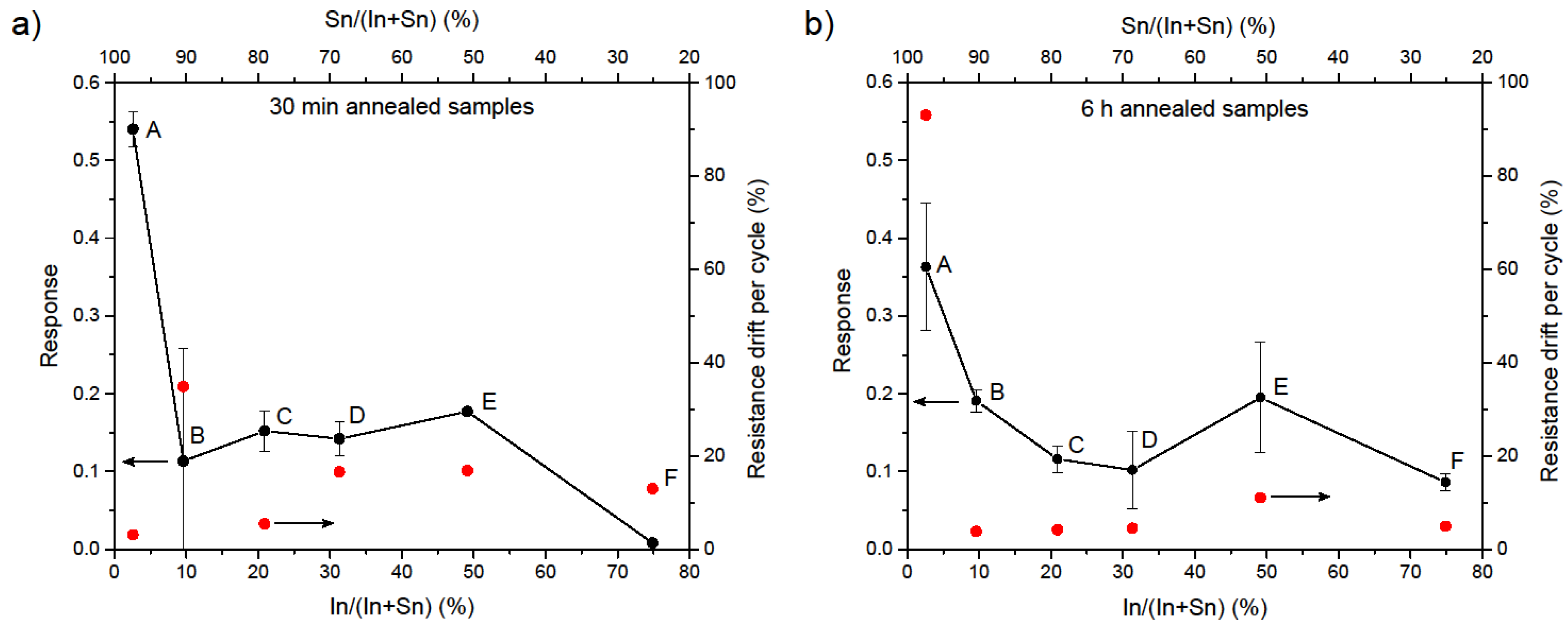
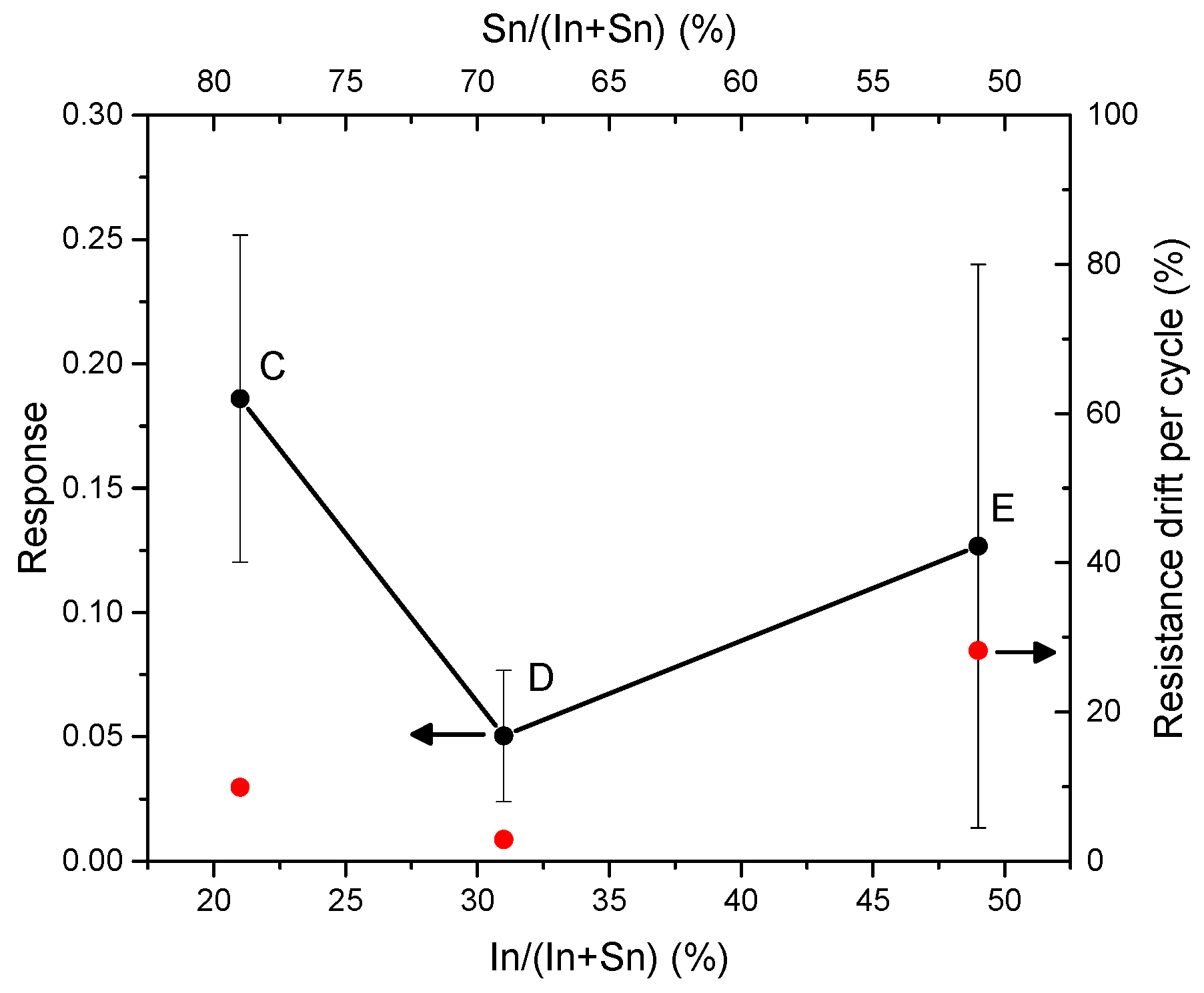
3.2. Acetaldehyde Sensing

Resistance changes were recorded for the In–Sn oxide films during controlled acetaldehyde gas exposure cycles. The underlying mechanism for the resistance change is proposed to be oxygen adsorption and dissociation with accompanying electron transfer reactions following oxidation of acetaldehyde at the film surface [7], as explained, e.g., by Kohl [24] and by Barsan and Weimar [25]. Specifically, atomic O fragments accept electrons from metal atoms, thus giving a decreased electron concentration in the film. Since the In–Sn oxide film is an n-type semiconductor, this leads to an increased film resistance. Acetaldehyde reacts with the adsorbed O on the film as
C2H4O + O(ads)→CH3COOH + e
resulting in the formation of acetic acid and back-donation of electrons to the film [5], thus producing a decreased film resistance.
The electrical response, S, of the gas sensor is defined as the change in resistance upon exposure to acetaldehyde gas divided by the initial resistance according to
S = R a i r R g a s R a i r
where Rgas and Rair are the resistance after exposure to acetaldehyde and synthetic air, respectively [26]. An average value of S over three measurement cycles was used in the analysis of our In–Sn oxide films. Another important parameter for the sensor is its resistance drift per gas exposure cycle, Rdrift, which is defined (in percent) as the resistance change in synthetic air from the beginning of the measurement (Rbegin) to the end of the measurement (Rend) divided by the number of exposure cycles nc, i.e.,
R d r i f t = | R e n d R b e g i n | R b e g i n × n c × 100 %
Three exposure cycles were used to obtain Rdrift, except for samples E and F, annealed for 30 min up to 400 °C where—due to contact problems—only one cycle was used in the analysis. Figure 6 shows an illustrative example of data taken at an operating temperature of 200 °C, specifically for sample F annealed at 400 °C for 6 h. Other samples had qualitatively similar responses to acetaldehyde exposure. Measurements were also performed at room temperature, 50 °C, 100 °C and 150 °C with 25 ppm of acetaldehyde exposure but with no measureable responses. Hence, the lowest practical operating temperature was chosen to be 200 °C and was employed in all gas response measurements reported below.
Figure 7 reports data for In–Sn oxide samples A–F, annealed at 400 °C for 30 min and 6 h, respectively, and exposed to 25 ppm of acetaldehyde. The data demonstrate a clear relation between the response to acetaldehyde exposure and the film composition. The most sensitive samples are those with the lowest In concentration. For samples A–D, annealed for 6 h, there is a trend of a decreasing S with the increasing In concentration up to about 30%. Samples B–E, annealed for 30 min, have rather similar responses lying in the 0.12–0.18 range. Rdrift is, in general, higher for samples annealed for 30 min than for 6 h, the exception being sample A. The XRD data in Figure 2 showed that samples A and B are crystalline with SnO2-like structure, whereas samples C and D are amorphous. Moreover, the grain sizes were smaller in SnO2-type films annealed at 30 min than those annealed for 6 h, as discussed above. Both factors are expected to influence S, with smaller crystals leading to higher S, and amorphous structures decreasing S due to impurity scattering. However, the uncertainties of the data in Figure 7 and the superimposed variations of sample properties prohibit conclusive explanations of the S trend. We note in Figure 7 that there is a slightly enhanced response of the sample with In/(In + Sn) close to 50%. Although our result lies within experimental uncertainties, this observation lends support to a similar result in work by Kemmler et al. [20], but with the important difference that our samples with intermediate In–Sn composition are amorphous. This may indicate that the conduction mechanism in these samples is dominated by impurity conduction, and that the enhancement observed by Kemmler et al. [20] is due to the crystallinity of their particles, which is not possible to obtain by DC magnetron sputtering.
Gas sensing responses for samples C, D and E, annealed at 500 °C for 12 h, were measured under the same conditions as before for 25 ppm of acetaldehyde. As discussed above, sample C subjected to this annealing treatment is transformed into nanocrystalline SnO2 with tetragonal structure, while samples D and E remain amorphous. Corresponding results are shown in Figure 8. Sample C then showed a higher response compared to after it had been annealed at 400 °C for 30 min and 6 h, while the resistance drift remained almost the same. In contrast, the responses decreased for samples D and E annealed at 500 °C. Correspondingly, the resistance drift per cycle decreased for sample D whereas it increased for sample E.
Further measurements were performed on samples with the highest responses to acetaldehyde exposure, viz., sample A annealed at 400 °C for 30 min and 6 h, and for samples B and E annealed at 400 °C for 6 h, in order to quantify their corresponding acetaldehyde detection limits. Figure 9 shows data on S and Rdrift for concentrations down to 200 ppb. The resistance values were smoothed by using a 50-point averaging algorithm, and the stated values represent an average over three cycles of exposure. Detectable sensor responses, well within the error limits, were documented down to 200 ppb of acetaldehyde at 200 °C for sample A annealed for 30 min and for sample B annealed for 6 h. Sample E, with about equal amounts of In and Sn, had a sensitivity that was an intermediate between those for the samples that could be used down to 200 ppb and it is expected to be sensitive to acetaldehyde at a similar level. The resistance drift for these samples was 1%–3% at concentrations below 1 ppm. It is noteworthy that the amorphous sample E performed almost as well as the SnO2-rich nanocrystalline samples. This indicates that an oxide with approximately equal amounts of In and Sn may be interesting as a gas sensor even in the easily obtained amorphous form. Further studies to elucidate the dominant conduction mechanism in those samples should be undertaken (e.g., whether or not impurity conduction is important, which might explain why the conductivity decreases with increasing crystallinity).

4. Conclusions

In–Sn oxide thin films with a wide range of compositions were prepared by reactive DC magnetron sputtering followed by annealing post-treatment. The films were tested for gas sensing at 200 °C upon exposure to acetaldehyde. Responses down to 200 ppb, together with small resistance drift between repeated gas exposures, were found in crystalline SnO2-like films and in amorphous films with similar amounts of In and Sn. Further annealing of amorphous films with high In concentration did not improve their gas sensing properties, and crystalline films with similar amounts of In and Sn were not possible to obtain even after annealing at 500 °C for 12 h. We have shown that a nanocrystalline gas sensing material with about 50% In concentration, as has previously been reported to be favorable for gas sensing [20], cannot easily be achieved by the annealing of DC magnetron sputtered films, even at a temperature as high as 500 °C. For our films prepared by DC magnetron sputtering, low In concentrations yielded the highest response, which appears to be associated with the tetragonal SnO2 structure, and depends critically on the structure and particle size of the films, as suggested by our conductance and XRD results.
The low-temperature operation and good response of amorphous films, together with their low resistance drift, which is a new finding in this work, nevertheless suggest that sputter-deposited In–Sn oxide films are of interest for air quality sensing and call for further scrutinized studies on the conduction mechanisms in In–Sn oxide films with intermediate In:Sn compositions.

Acknowledgments

Financial support was received from the European Research Council under the European Community’s Seventh Framework Program (FP7/2007–2013)/ERC, Grant Agreement No. 267234 (“GRINDOOR”). The authors are grateful to Daniel Primetzhofer from the Department of Physics and Astronomy of Uppsala University for RBS measurements.

Author Contributions

Umut Cindemir carried out gas sensing measurements, material characterization measurements (SEM, EDS, XRD, conduction), performed the data treatment and wrote the original manuscript. Pia C. Lansåker prepared samples, performed material characterization measurements (XRD, XPS, thickness) and contributed with writing. Lars Österlund, Gunnar A. Niklasson and Claes-Göran Granqvist conceived the idea of the work, designed the structure of the article and revised the manuscript.

Conflicts of Interest

The authors declare no conflict of interest. The founding sponsors had no role in the design of the study; in the collection, analyses, or interpretation of data; in the writing of the manuscript, and in the decision to publish the results.

Abbreviations

The following abbreviations are used in this manuscript:
DC
Direct current
VOC
Volatile organic compound
SMOX
Semiconducting metal oxide
XPS
X-ray photoelectron spectroscopy
EDS
Energy-dispersive X-ray spectroscopy
SEM
Scanning electron microscopy
RBS
Rutherford backscattering spectroscopy
XRD
X-ray diffraction
ICDD
International Centre for Diffraction Data

References

  1. Leech, J.A.; Nelson, W.C.; Burnett, R.T.; Aaron, S.; Raizenne, M.E. It’s about time: A comparison of Canadian and American time-activity patterns. J. Expo. Anal. Environ. Epidemiol. 2002, 12, 427–432. [Google Scholar] [CrossRef] [PubMed]
  2. Murphy, M. Sick Building Syndrome and the Problem of Uncertainty: Environmental Politics, Technoscience, and Women Workers; Duke University Press: Durham, NC, USA, 2006. [Google Scholar]
  3. Eckert, M.; Fleischmann, G.; Jira, R.; Bolt, H.M.; Golka, K. Acetaldehyde. In Ullmann’s Encyclopedia of Industrial Chemistry; Wiley-VCH: Weinheim, Germany, 2006. [Google Scholar] [CrossRef]
  4. Grosjean, D.; Miguel, A.H.; Tavares, T.M. Urban air pollution in Brazil: Acetaldehyde and other carbonyls. Atmos. Environ. B Urban Atmos. 1990, 24, 101–106. [Google Scholar] [CrossRef]
  5. Kimmerer, T.W.; Kozlowski, T.T. Ethylene, ethane, acetaldehyde, and ethanol production by plants under stress. Plant Physiol. 1982, 69, 840–847. [Google Scholar] [CrossRef] [PubMed]
  6. Pesis, E.; Dvir, O.; Feygenberg, O.; Ben Arie, R.; Ackerman, M.; Lichter, A. Production of acetaldehyde and ethanol during maturation and modified atmosphere storage of litchi fruit. Postharvest Biol. Technol. 2002, 26, 157–165. [Google Scholar] [CrossRef]
  7. Barsan, N.; Koziej, D.; Weimar, U. Metal oxide-based gas sensor research: How to? Sens. Actuators B Chem. 2007, 121, 18–35. [Google Scholar] [CrossRef]
  8. Das, S.; Jayaraman, V. SnO2: A comprehensive review on structures and gas sensors. Progr. Mater. Sci. 2014, 66, 112–255. [Google Scholar] [CrossRef]
  9. Miller, D.R.; Akbar, S.A.; Morris, P.A. Nanoscale metal oxide-based heterojunctions for gas sensing: A review. Sens. Actuators B Chem. 2014, 204, 250–272. [Google Scholar] [CrossRef]
  10. Rickerby, D.G.; Skouloudis, A.N. Application of nanocrystalline metal oxide gas sensors for air quality monitoring. Int. J. Nanotechnol. 2014, 11, 583–593. [Google Scholar] [CrossRef]
  11. Zhang, G.; Liu, M. Effect of particle size and dopant on properties of SnO2-based gas sensors. Sens. Actuators B Chem. 2000, 69, 144–152. [Google Scholar] [CrossRef]
  12. Giberti, A.; Carotta, M.C.; Fabbri, B.; Gherardi, S.; Guidi, V.; Malagù, C. High-sensitivity detection of acetaldehyde. Sens. Actuators B Chem. 2012, 174, 402–405. [Google Scholar] [CrossRef]
  13. Tang, W.; Wang, J.; Yao, P.; Li, X. A microscale formaldehyde gas sensor based on Zn2SnO4/SnO2 and produced by combining hydrothermal synthesis with post-synthetic heat treatment. J. Mater. Sci. 2014, 49, 1246–1255. [Google Scholar] [CrossRef]
  14. Liu, L.; Li, X.; Dutta, P.K.; Wang, J. Room temperature impedance spectroscopy-based sensing of formaldehyde with porous TiO2 under UV illumination. Sens. Actuators B Chem. 2013, 185, 1–9. [Google Scholar] [CrossRef]
  15. Castro-Hurtado, I.; Mandayo, G.G.; Castaño, E. Conductometric formaldehyde gas sensors. A review: From conventional films to nanostructured materials. Thin Solid Films 2013, 548, 665–676. [Google Scholar] [CrossRef]
  16. Tian, S.; Ding, X.; Zeng, D.; Zhang, S.; Xie, C. Pore-size-dependent sensing property of hierarchical SnO2 mesoporous microfibers as formaldehyde sensors. Sens. Actuators B Chem. 2013, 186, 640–647. [Google Scholar] [CrossRef]
  17. Taguchi, N. Gas Detecting Element and Method of Making It. US Patent No. 3664795A, 1972. [Google Scholar]
  18. Luyo, C.; Ionescu, R.; Reyes, L.F.; Topalian, Z.; Estrada, W.; Llobet, E.; Granqvist, C.G.; Heszler, P. Gas sensing response of NiO nanoparticle films made by reactive gas deposition. Sens. Actuators B Chem. 2009, 138, 14–20. [Google Scholar] [CrossRef]
  19. Sberveglieri, G.; Faglia, G.; Groppelli, S.; Nelli, P. Methods for the preparation of NO, NO2 and H2 sensors based on tin oxide thin films, grown by means of the r.f. magnetron sputtering technique. Sens. Actuators B Chem. 1992, 8, 79–88. [Google Scholar] [CrossRef]
  20. Kemmler, J.A.; Pokhrel, S.; Birkenstock, J.; Schowalter, M.; Rosenauer, A.; Bârsan, N.; Weimar, U.; Mädler, L. Quenched, nanocrystalline In4Sn3O12 high temperature phase for gas sensing applications. Sens. Actuators B Chem. 2012, 16, 740–747. [Google Scholar] [CrossRef]
  21. Mayer, M. SIMNRA, a simulation program for the analysis of NRA, RBS and ERDA. AIP Conf. Proc. 1999, 475, 541–544. [Google Scholar]
  22. Cullity, B.D.; Stock, S.R. Elements of X-ray Diffraction; Pearson: Upper Saddle River, NJ, USA, 2001. [Google Scholar]
  23. Isomäki, I.; Hämäläinen, M.; Gierlotka, W.; Onderka, B.; Fitzner, K. Thermodynamic evaluation of the In–Sn–O system. J. Alloys Cpds. 2006, 422, 173–177. [Google Scholar] [CrossRef]
  24. Kohl, D. Function and applications of gas sensors. J. Phys. D Appl. Phys. 2001, 34, R125–R149. [Google Scholar] [CrossRef]
  25. Barsan, N.; Weimar, U. Conduction model of metal oxide gas sensors. J. Electroceram. 2001, 7, 143–167. [Google Scholar] [CrossRef]
  26. D’Amico, A.; Di Natale, C. A contribution on some basic definitions of sensors properties. IEEE Sensors J. 2001, 1, 183–190. [Google Scholar] [CrossRef]
Figure 1. Schematic drawing of the gas sensor setup. Contacts were made by Ag paste, which was also used to attach glass substrates on the heater. Dimensions of the sensors were 20 mm × 8 mm × 1 mm, and the widths of the contacts were approximately 2 mm.
Coatings 06 00019 g001
Figure 2. SEM images of sample E, characterized in Table 2, after annealing for 30 min (a) and 6 h (b).
Coatings 06 00019 g002
Figure 3. X-ray diffraction patterns of samples characterized in Table 2. All samples were annealed at 400 °C for 30 min (a) and 6 h (b). The diffraction peaks for the crystalline samples were assigned to SnO2 (samples A and B) and In2O3 (sample F). The diffractograms are shifted along the ordinate axis for clarity.
Coatings 06 00019 g003
Figure 4. X-ray diffraction patterns of samples C, D and E, characterized in Table 2, after annealing at 500 °C for 12 h. Sample C exhibits diffraction peaks corresponding to SnO2. Dashed lines indicate the location of diffraction peaks for Ag, which was used for electrodes. Further EDS analysis proved that films are not contaminated with Ag.
Coatings 06 00019 g004
Figure 5. Electrical conductivity at 200 °C for samples, characterized in Table 2, with varying In and Sn contents and different annealing procedures. Data points are joined by straight lines for clarity.
Coatings 06 00019 g005
Figure 6. Electrical resistance vs. time measured at 200 °C for sample F, characterized in Table 2, annealed for 6 h at 400 °C. Data were taken for alternating exposure to 25 ppm of acetaldehyde and synthetic air. The various symbols refer to Equations (2) and (3).
Coatings 06 00019 g006
Figure 7. Response (black symbols) and resistance drift (red symbols) per acetaldehyde exposure cycle for samples A–F, characterized in Table 2, with increasing In content on the abscissa. Data are shown for samples annealed at 400 °C for 30 min (a) and 6 h (b), and the recordings were performed with 25 ppm of acetaldehyde at 200 °C as illustrated in Figure 6. Vertical bars signify experimental uncertainties (standard deviations). Symbols indicating measured results are connected by straight lines for convenience. Arrows indicate applicable vertical axis.
Coatings 06 00019 g007
Figure 8. Response (black symbols) and resistance drift (red symbols) per acetaldehyde exposure cycle for the samples C, D and E, characterized in Table 2, after annealing at 500 °C for 12 h, with increasing In content on the abscissa. Responses to 25 ppm of acetaldehyde were recorded at 200 °C. Arrows indicate applicable vertical axis.
Coatings 06 00019 g008
Figure 9. Response (a) and resistance drift per exposure cycle (b) as a function of acetaldehyde concentration for representative sensor samples characterized in Table 2. The annealing times are indicated in the legends, and the annealing temperature was 400 °C. Vertical bars signify experimental uncertainties (standard deviations). Symbols indicating measured results are connected by straight lines for convenience.
Coatings 06 00019 g009
Table 1. Deposition conditions for dual-target sputtering to make In–Sn oxide films, showing gas pressure p, argon flow rate fAr, oxygen flow rate fO2 and power P to the targets.
Samplep [Pa]fAr [mL/min]fO2 [mL/min]Target 1
In(3 wt.%)–Sn(97 wt.%)
P [W]
Target 2
In(90 wt.%)–Sn(10 wt.%)
P [W]
A0.582517.255
B0.582513.04411
C0.582512.03322
D0.53259.02233
E0.53259.01144
F0.53259.055
Table 2. Film thickness d and composition of In–Sn oxide films in as-deposited and annealed states. Different techniques were used to determine the elemental contents, as explained in the main text.
Sampled [nm]In/[In+Sn](%)
(as-deposited) (XPS)
Sn/[In+Sn](%)
(as-deposited) (XPS)
In/[In+Sn](%)
(6 h annealed) (EDS)
Sn/[In+Sn](%)
(6 h annealed) (EDS)
O [at. %]
(as-deposited) (RBS)
O [at. %]
(6 h annealed) (RBS)
A1703974966563
B180109012886565
C190217924766566
D150316935656566
E120495152486466
F110752576246460

