
Combined Terahertz Pulsed Imaging and Optical Coherence Tomography Detection Method for Multiple Defects in Thermal Barrier Coatings

Abstract
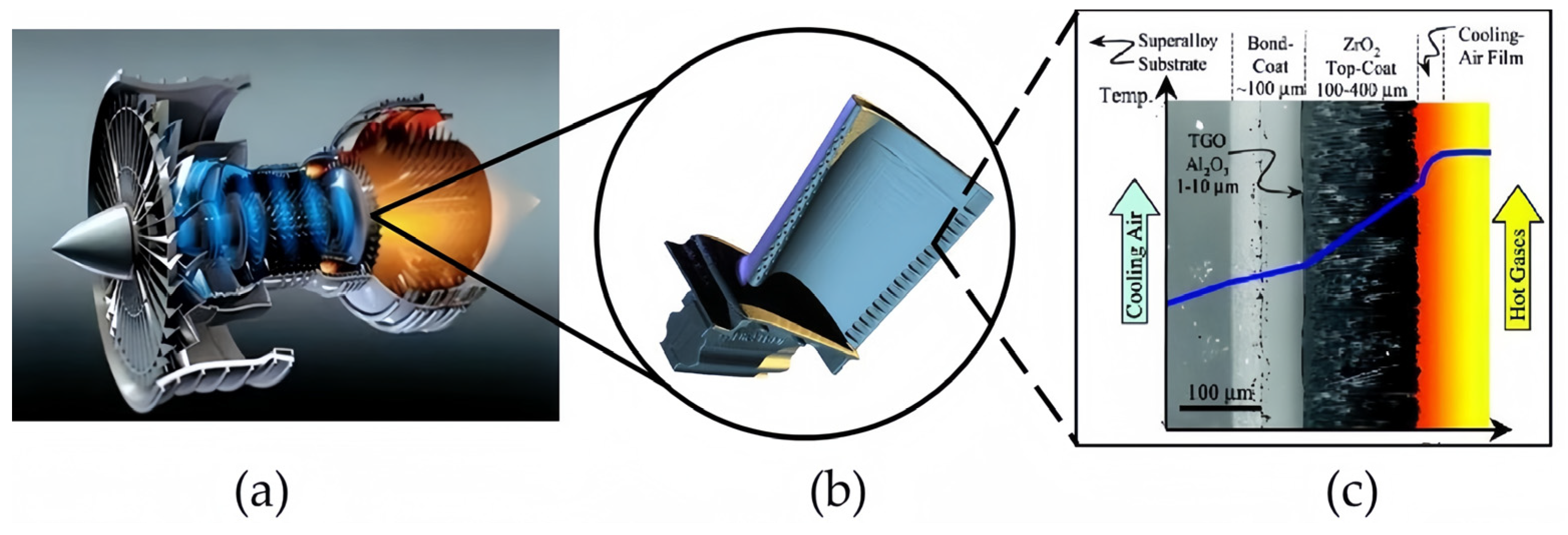
:1. Introduction
2. Methods and Materials
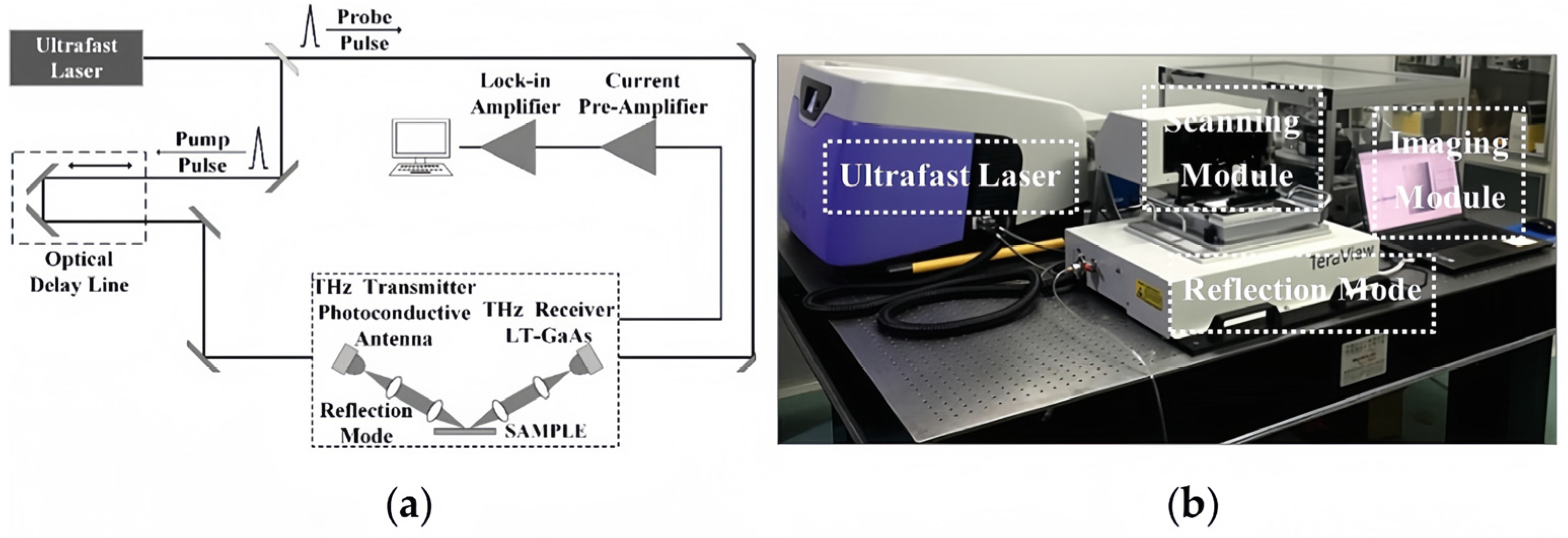
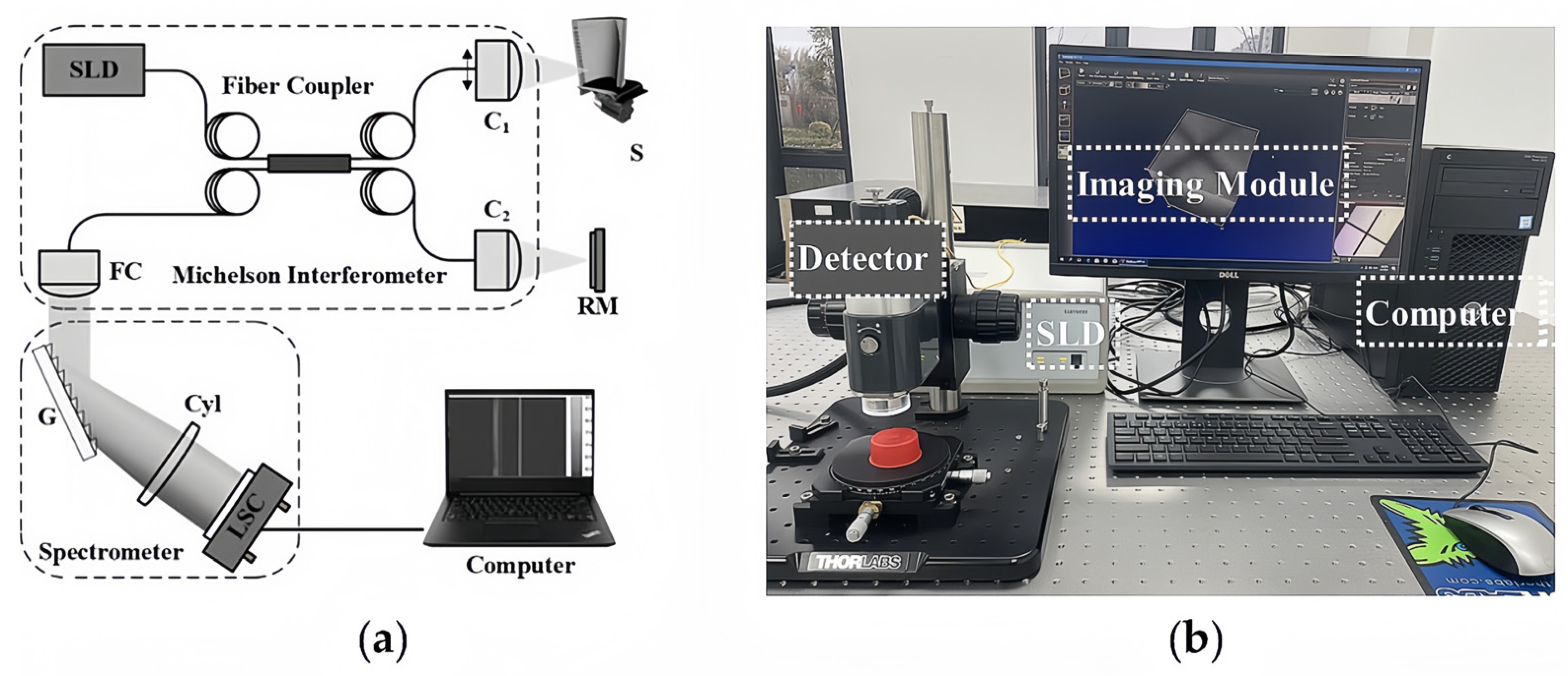
2.1. Methods
2.2. Sample Preparation
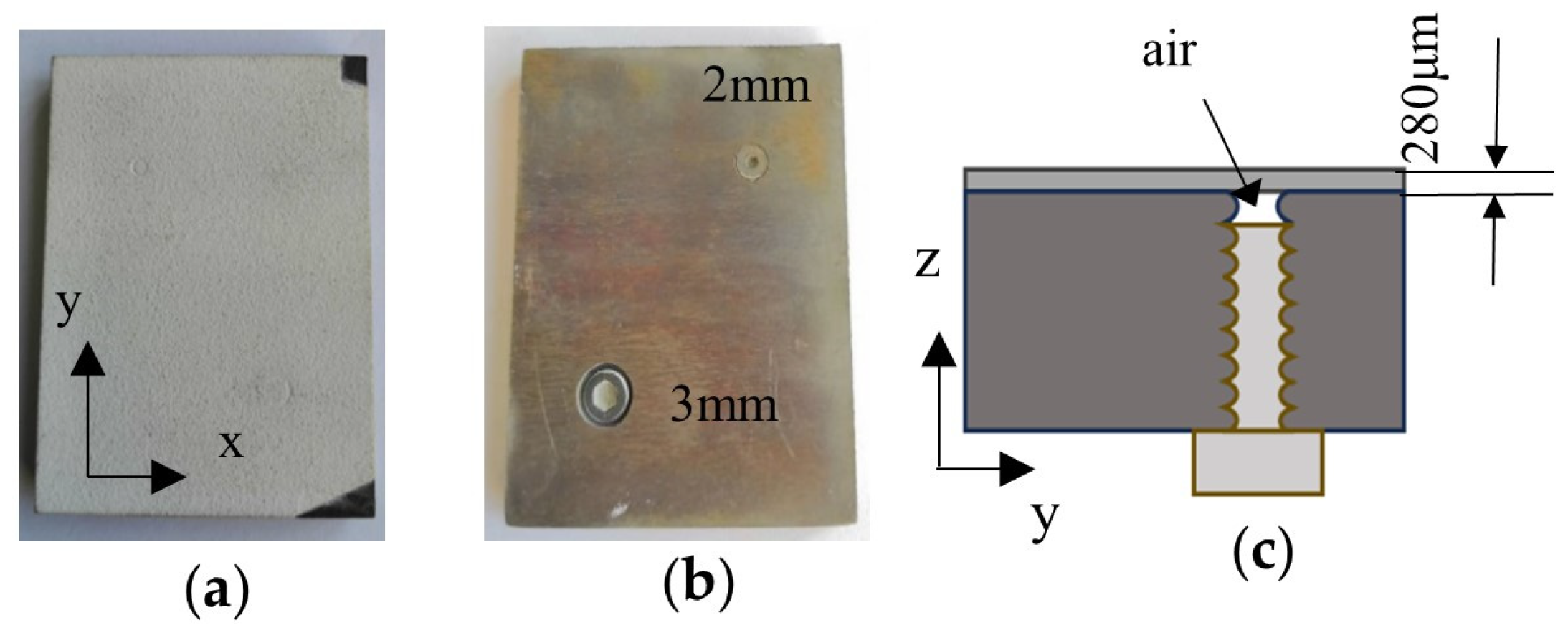
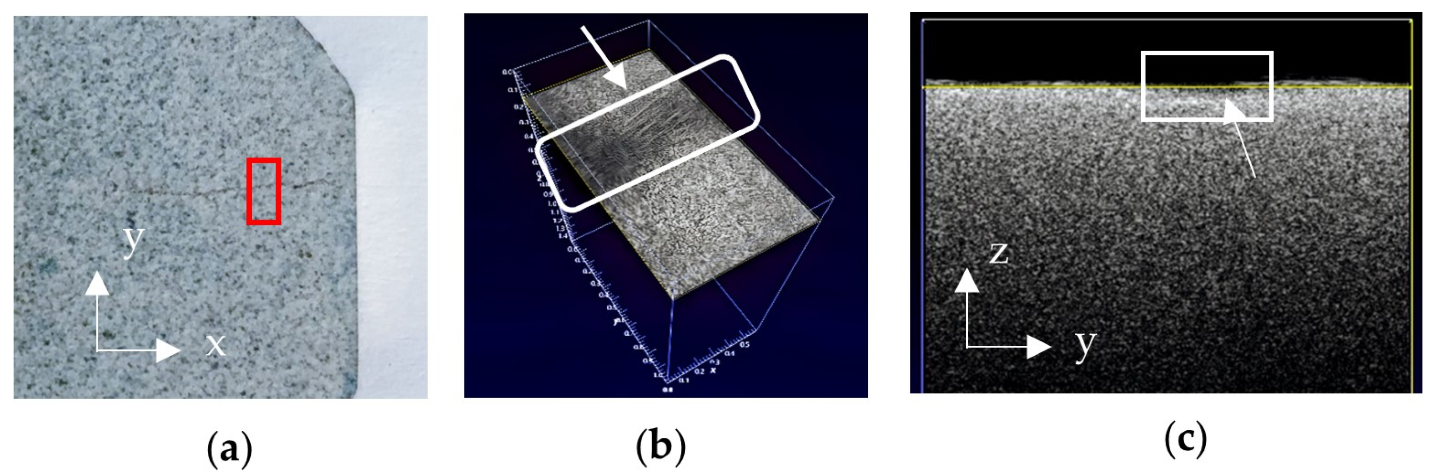
2.2.1. Internal Debonding Cracks
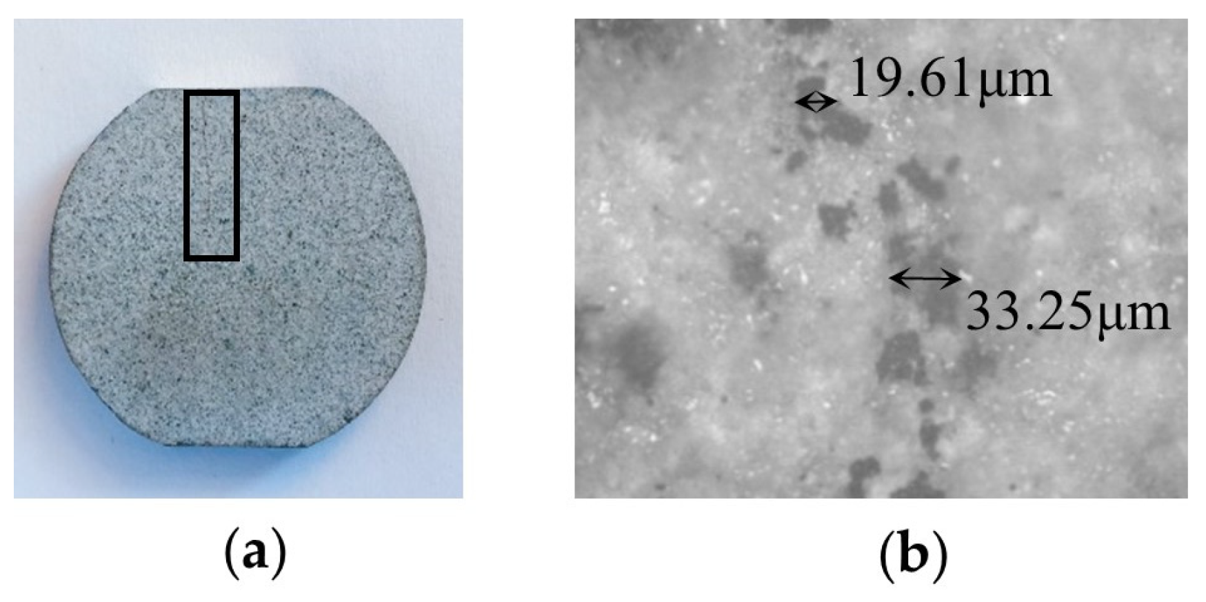
2.2.2. Surface High-Temperature Cracks
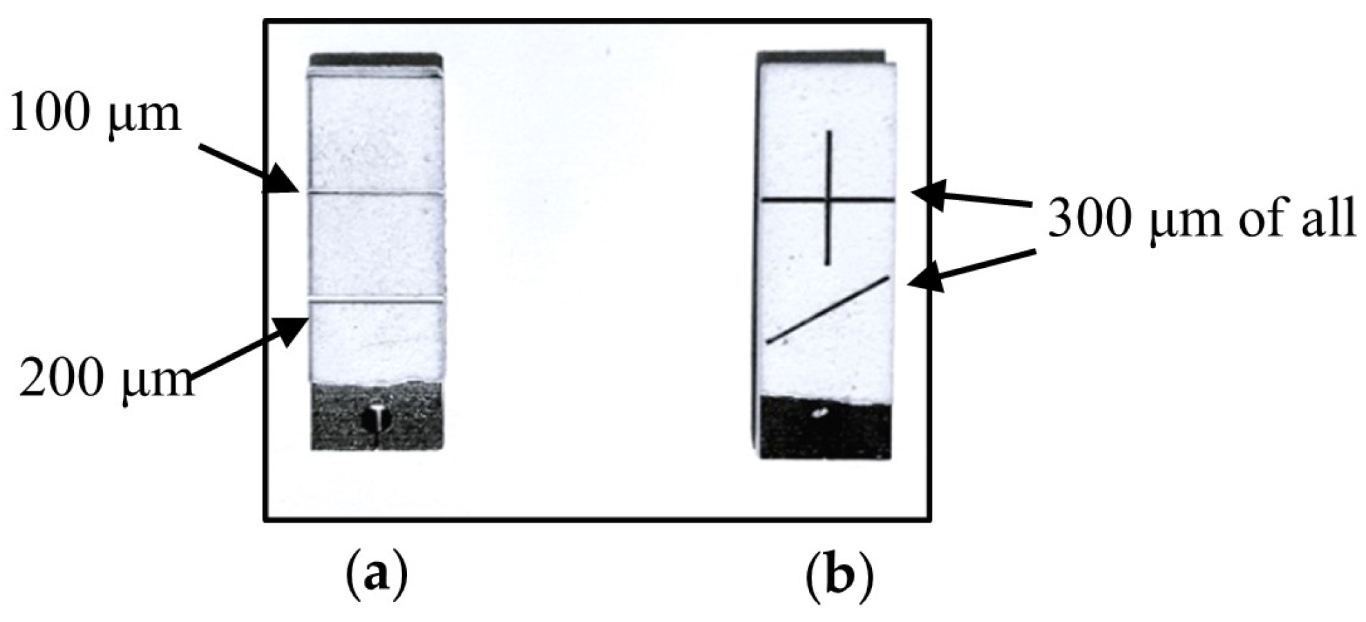
2.2.3. Etched Cracks
3. Experiment
3.1. OCT and TPI Penetration Ability Experiment
3.1.1. Samples without Defects
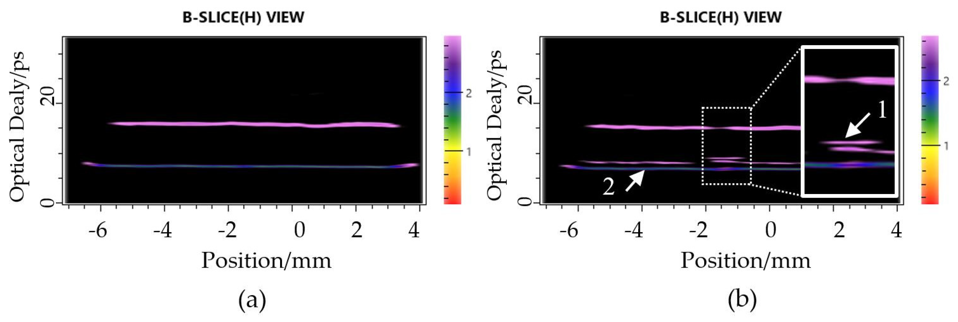
3.1.2. Samples with Internal Debonding Cracks
3.2. Resolution Ability Experiment of OCT and TPI
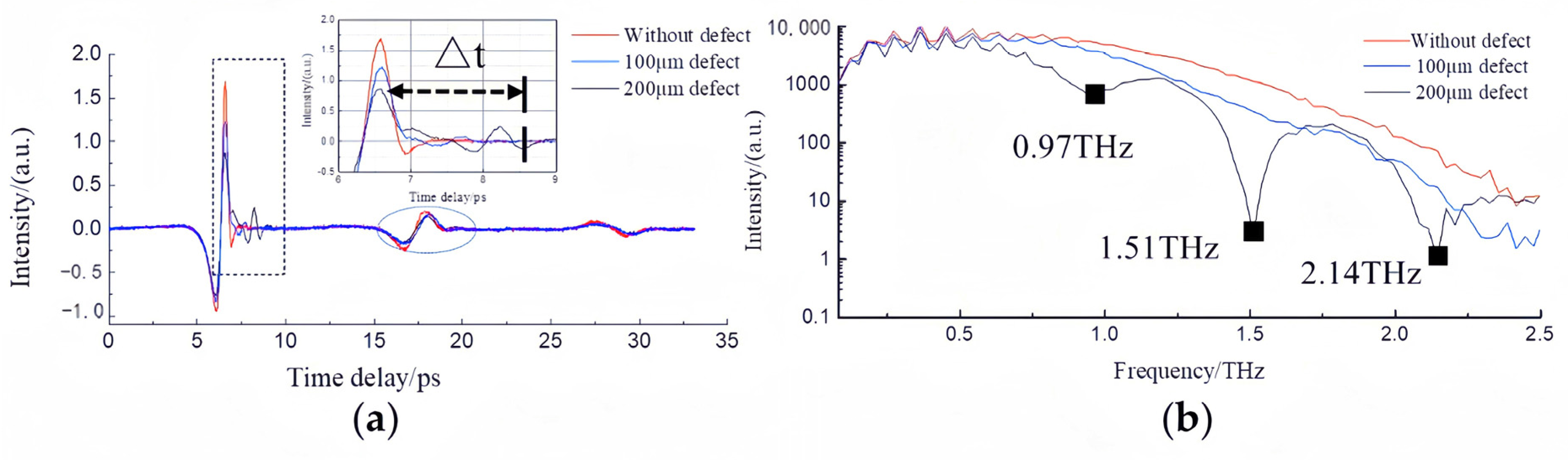
3.2.1. Surface High-Temperature Cracks
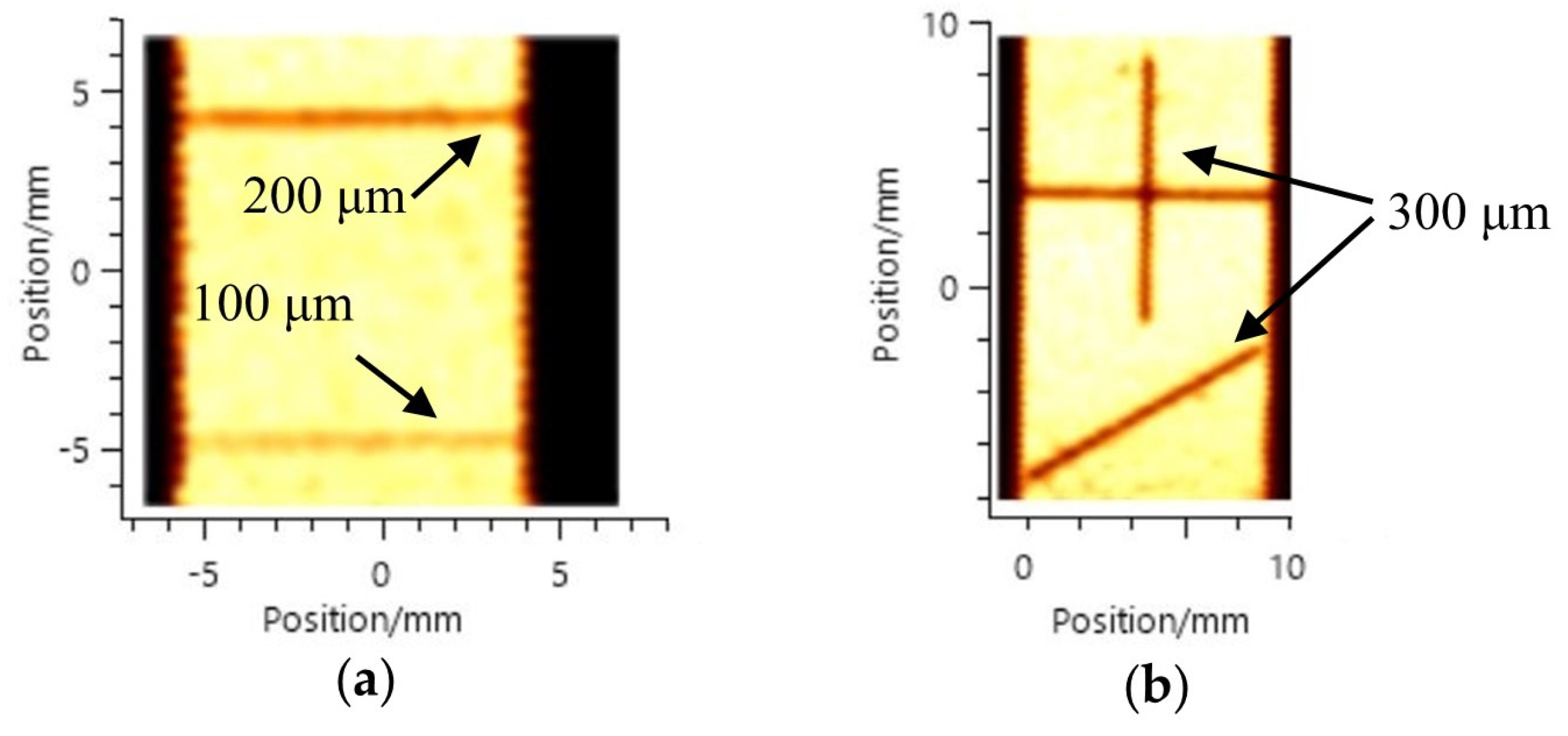
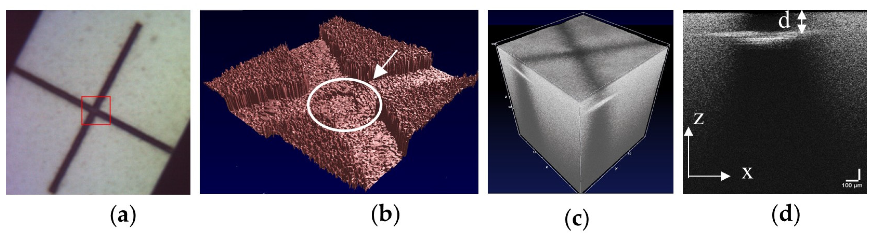
3.2.2. Etched Cracks
4. Conclusions
- (1)
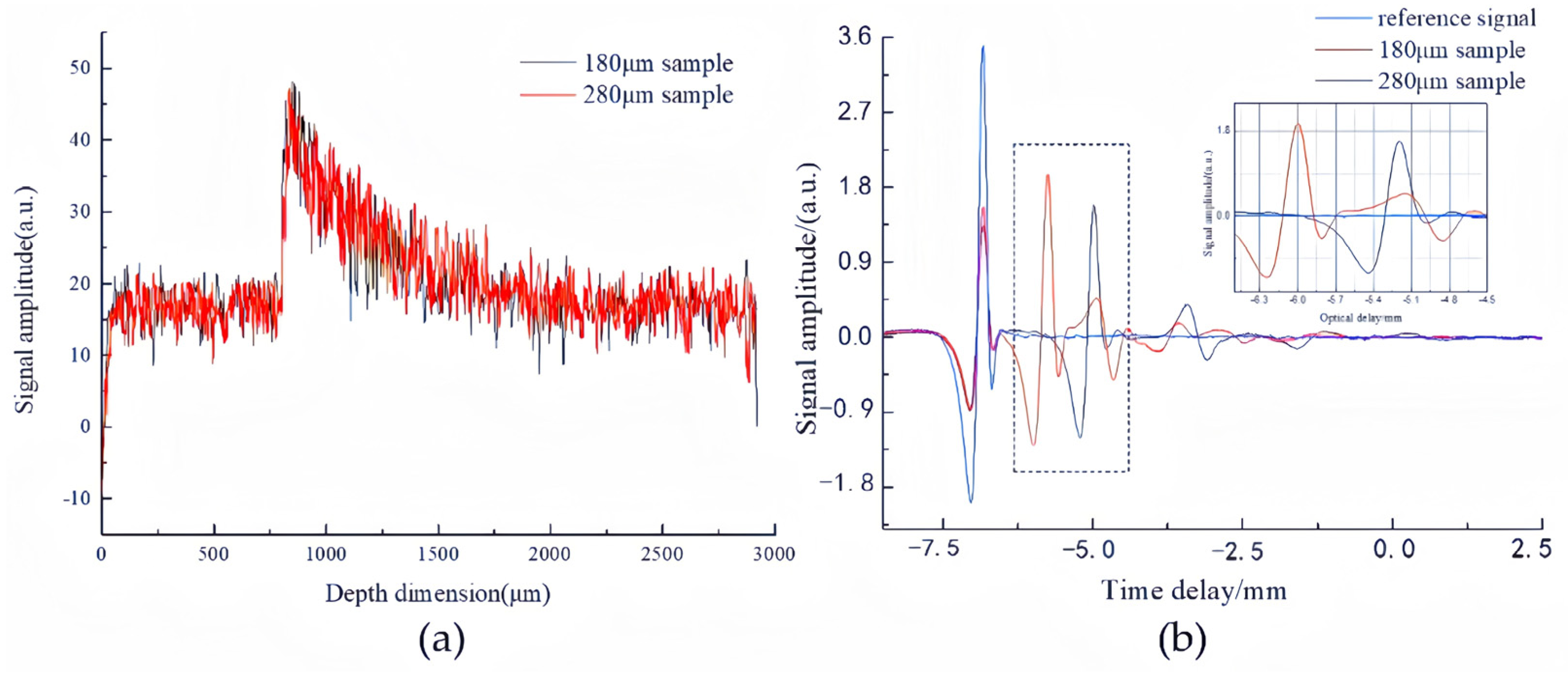
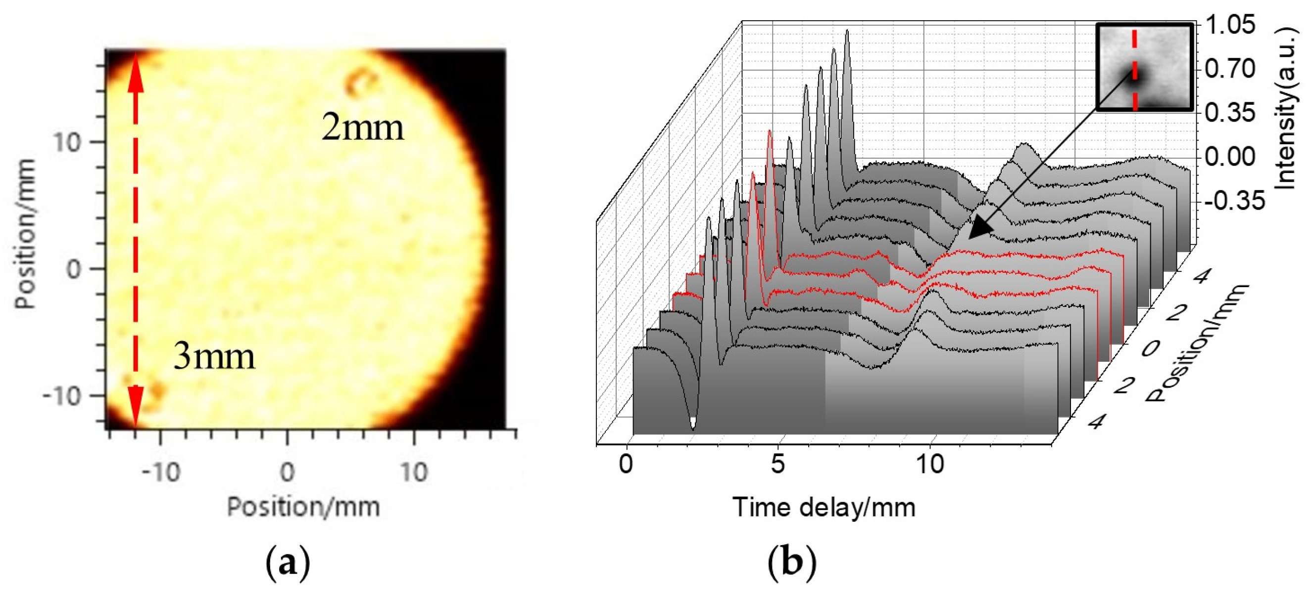
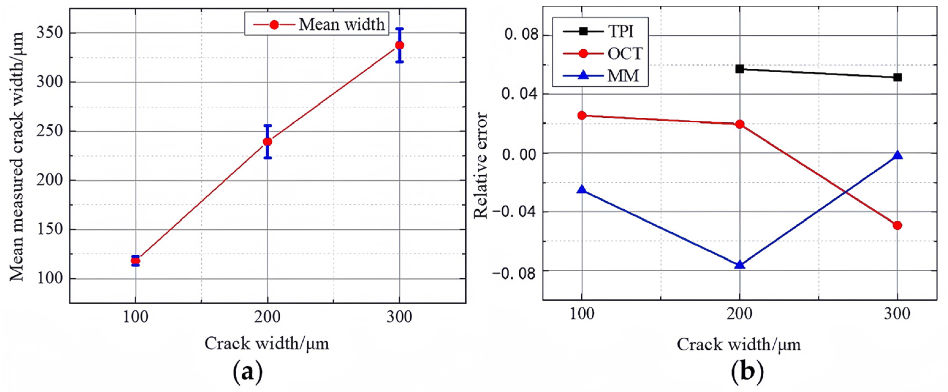
- A TPI system was used to detect the typical defects of the TBCs, such as debonding defects and etched cracks. It was verified that the size of debonding defects larger than 2 mm and the etched defects above 200 μm could achieve good qualitative and quantitative measurement results (100 μm defect can be hard to obtain). It was also verified that the thickness of the penetrable TC layer exceeds 500 μm. However, the detection of high-temperature oxide cracks by TPI failed because of the resolution limitation of TPI.
- (2)
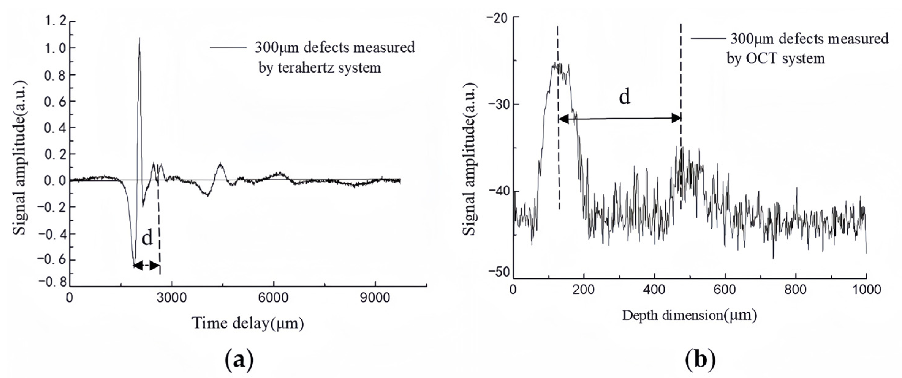
- The typical defects of TBCs (surface etched cracks and high-temperature oxidation cracks) were evaluated by the OCT system. The results show that the high-temperature oxidation cracks can be detected by OCT with short coherence length and higher resolution, and the repeated etched circular pits of surface etched cracks can be observed better than by the TPI system. OCT can also easily measure the width and depth of etched cracks on 100 μm surfaces, with a relative error of only 5%. The high precision measurement of OCT systems complements the TPI detection information characteristics, but it can only complete the shallow surface crack measurement. This conclusion is demonstrated objectively by comparing the one-dimensional time-domain signal of terahertz with the one-dimensional time-domain signal of OCT.
Author Contributions
Funding
Institutional Review Board Statement
Informed Consent Statement
Data Availability Statement
Acknowledgments
Conflicts of Interest
References
- Wen, F.J.; Long, Z.; Xing, Z.G.; Guo, W.L.; Huang, Y.F. Research on Damage Behavior of Thermal Barrier Coatings Based on Acoustic Emission Technology. Nondestruct. Test. Eval. 2023, 38, 67–89. [Google Scholar] [CrossRef]
- Sun, F.S.; Fan, M.B.; Cao, B.H.; Zheng, D.D.; Liu, H.; Liu, L. Terahertz Based Thickness Measurement of Thermal Barrier Coatings Using Long Short-Term Memory Networks and Local Extrema. IEEE Trans. Ind. Inform. 2022, 18, 2508–2517. [Google Scholar] [CrossRef]
- Ye, D.D.; Wang, W.Z.; Zhou, H.T.; Fang, H.J.; Huang, J.B.; Li, Y.J.; Gong, H.H.; Li, Z. Characterization of Thermal Barrier Coatings Microstructural Features Using Terahertz Spectroscopy. Surf. Coat. Technol. 2020, 394, 125836–125846. [Google Scholar] [CrossRef]
- Zhang, Z.H.; Huang, Y.; Zhong, S.C.; Lin, T.L.; Zhong, Y.J.; Zeng, Q.M.; Nsengiyumva, W.; Yu, Y.J.; Peng, Z.K. Time of Flight Improved Thermally Grown Oxide Thickness Measurement with Terahertz Spectroscopy. Front. Mech. Eng. 2022, 17, 49–61. [Google Scholar] [CrossRef]
- Sun, F.Z.; Cao, B.H.; Fan, M.B.; Liu, L. Physics-Based Deep Learning Framework for Terahertz Thickness Measurement of Thermal Barrier Coatings. SSRN Electron. J. 2023, in press. [CrossRef]
- Martin, E.; Larato, C.; Clément, A.; Saint-Paul, M. Detection of delaminations in sub-wavelength thick multi-layered packages from the local temporal coherence of ultrasonic signals. NDT E Int. 2008, 41, 280–291. [Google Scholar] [CrossRef]
- Zhang, X.; Augereau, F.; Laux, D.; Le Clezio, E.; Ismaili, N.A.; Kuntz, M.; Despaux, G. Non-destructive Testing of Paint Coatings on Steel Plates by Ultrasonic Reflectometry. J. Nondestruct. Eval. 2014, 33, 504–514. [Google Scholar] [CrossRef]
- Tu, W.L.; Zhong, S.C.; Xu, Y.Q. Terahertz Quantitative Nondestructive Evaluation of Marine Protective Coating. Ship Eng. 2017, 02, 79–85. [Google Scholar]
- He, Y.Z.; Tian, G.Y.; Pan, M.C.; Chen, D.X.; Zhang, H. An Investigation into Eddy Current Pulsed Thermography for Detection of Corrosion Blister. Corros. Sci. 2014, 78, 1–6. [Google Scholar] [CrossRef]
- Dong, L.H.; Guo, W.; Wang, H.D.; Xing, Z.G.; Feng, F.Z.; Wang, B.Z.; Gao, Z.F. Inspection of interface debonding in thermal barrier coatings using pulsed thermography. Ac-Ta Aeronaut. Et Astronaut. Sin. 2019, 40, 288–297. [Google Scholar]
- Liu, Z.W.; Jiao, D.C.; Shi, W.X.; Xie, H.M. Linear Laser Fast Scanning Thermography NDT for Artificial Disbond Defects in Thermal Barrier Coatings. Opt. Express 2017, 25, 31789–31800. [Google Scholar] [CrossRef] [PubMed]
- Li, J.C.; He, Q.; Lv, Y.F.; Liang, L.K. Research Progress on Non-destructive Testing Method of Thermal Barrier Coatings. China Surf. Eng. 2019, 32, 16–26. [Google Scholar]
- Ma, Z.Y.; Zhao, Y.; Luo, Z.B.; Lin, L. Ultrasonic Characterization of Thermally Grown Oxide in Thermal Barrier Coating by Reflection Coefficient Amplitude Spectrum. Ultrasonics 2014, 54, 1005–1009. [Google Scholar] [CrossRef]
- Li, Y.; Chen, Z.M.; Mao, Y.; Qi, Y. Quantitative Evaluation of Thermal Barrier Coating Based on Eddy Current Technique. NDT E Int. Indep. Nondestruct. Test. Eval. 2012, 50, 29–35. [Google Scholar]
- Grégoire, W.; Shklover, V.; Steurer, W.; Bachegowda, S.; Bossmann, H.P. Phase Evolution in Yttria-Stabilized Zirconia Thermal Barrier Coatings Studied by Rietveld Refinement of X-Ray Powder Diffraction Patterns. J. Am. Ceram. Soc. 2010, 90, 2935–2940. [Google Scholar]
- Knipe, K.; Manero, A.; Siddiqui, S.F.; Meid, C.; Wischek, J.; Okasinski, J.; Almer, J.; Karlsson, A.M.; Bartsch, M.; Raghavan, S. Strain response of thermal barrier coatings captured under extreme engine environments through synchrotron X-ray diffraction. Nat. Commun. 2014, 5, 4559–4565. [Google Scholar] [CrossRef] [PubMed]
- Tang, Q.J.; Dai, J.M.; Liu, J.Y.; Liu, C.S.; Liu, Y.L.; Ren, C.P. Quantitative Detection of Defects Based on Markov-PCA-BP Algorithm Using Pulsed Infrared Thermography Technology. Infrared Phys. Technol. 2016, 77, 144–148. [Google Scholar] [CrossRef]
- Newaz, G.; Chen, X.Q. Progressive Damage Assessment in Thermal Barrier Coatings Using Thermal Wave Imaging Technique. Surf. Coat. Technol. 2005, 190, 7–14. [Google Scholar] [CrossRef]
- Sterczewski, L.A.; Westberg, J.; Yang, Y.; Burghoff, D.; Reno, J.; Hu, Q.; Wysocki, G. Terahertz hyperspectral imaging with dual chip-scale combs. Optica 2019, 6, 766. [Google Scholar] [CrossRef]
- Cao, B.H.; Li, H.X.; Fan, M.B.; Sun, F.S.; Ye, B. Model-Driven Terahertz Image Reconstruction Method for Debonding Defects in Thermal Barrier Coatings. Appl. Opt. 2023, 62, 9343–9352. [Google Scholar] [CrossRef]
- Zhong, S.C. Progress in Terahertz Nondestructive Testing: A review. Front. Mech. Eng. 2019, 14, 273–281. [Google Scholar] [CrossRef]
- Liu, Z.H.; Man, R.X.; Wang, K.X.; Wu, Y.H. Nondestructive Evaluation of Coating Defects and Uniformity Based on Terahertz Time-Domain Spectroscopy. Mater. Eval. 2022, 80, 34–43. [Google Scholar] [CrossRef]
- Luo, M.T.; Zhong, S.C.; Yao, L.G.; Tu, W.L.; Chen, W.Q. Thin Thermally Grown Oxide Thickness Detection In thermal Barrier Coatings Based on SWT-BP Neural network Algorithm and Terahertz Technology. Appl. Opt. 2020, 59, 4097–4104. [Google Scholar] [CrossRef] [PubMed]
- Xu, Y.F.; Wang, X.Y.; Zhong, S.C.; Zhang, L.Y.; Chen, X.F. Location and Separation of Terahertz Echo Signal of TBCs Based on Sparse Representation Method. J. Mech. Eng. 2023, 59, 9–19. [Google Scholar]
- Huang, D.; Swanson, E.A.; Lin, C.P.; Schuman, J.S.; Stinson, W.G.; Chang, W.; Hee, M.R.; Flotte, T.; Gregory, K.W.; Puliafito, C.A.; et al. Optical Coherence Tomography. Science 1991, 254, 1178–1181. [Google Scholar] [CrossRef] [PubMed]
- Ellingson, W.A.; Lipanovich, R.; Hopson, S.; Visher, R. Nondestructive Evaluation Methods for High Temperature Ceramic Coatings. Ceram. Eng. Sci. Proc. 2006, 3, 207–214. [Google Scholar]
- Alsayed, E.Z.; Sadr, A.; Nakashima, S.; Hariri, I. Demineralization Prevention by Enamel Resin Coating: Optical Coherence Tomography Evaluation. In Proceedings of the IADR/AADR/CADR General Session and Exhibition 2013, Seattle, DC, USA, 23 March 2013. [Google Scholar]
- Bochenek, K.; Wglewski, W.; Strojny-Ndza, A.; Pietrzak, K.; Chmielewski, T.; Chmielewski, M.; Basista, M. Microstructure, Mechanical, and Wear Properties of NiCr-Re-Al2O3 Coatings Deposited by HVOF, Atmospheric Plasma Spraying, and Laser Cladding. J. Therm. Spray Technol. 2022, 31, 1609–1633. [Google Scholar] [CrossRef]
- Wang, L.; Yang, J.L.; Ni, J.X.; Liu, C.G.; Zhong, X.H.; Shao, F.; Zhao, H.; Tao, S.Y.; Wang, Y.H. Influence of Cracks in APS-TBCs on Stress Around TGO During Thermal Cycling: A Numerical Simulation Study. Surf. Coat. Technol. 2016, 285, 98–112. [Google Scholar] [CrossRef]
- Sachinlal, A.; Nithin, P.; Krishnan, B. Nondestructive Evaluation of Aircraft Stealth Coating by Terahertz-Time Domain Spectroscopy: Experimental and Numerical Investigation. Nondestruct. Test. Eval. 2023, in press. [CrossRef]
- Zhong, H.; Xu, J.; Xie, X.L.; Yuan, T.; Reightler, R.; Madaras, E.I.; Zhang, X.C. Nondestructive Defect Identification with Terahertz Time-of-Flight Tomography. IEEE Sens. J. 2005, 5, 203–208. [Google Scholar] [CrossRef]
- Xu, J.; Zhang, X. Terahertz Science, Technology and Application; Peking University Press: Beijing, China, 2007; pp. 69–70. [Google Scholar]
- Tu, W.L.; Zhong, S.C.; Incecik, A.; Fu, X.B. Defect Feature Extraction of Marine Protective Coatings by Terahertz Pulsed Imaging. Ocean Eng. 2018, 155, 382–391. [Google Scholar] [CrossRef]
- Niwa, M.; Hiraishi, Y.; Terada, K. Evaluation of Coating Properties of Enteric-Coated Tablets Using Terahertz Pulsed Imaging. Pharm. Res. 2014, 31, 2140–2151. [Google Scholar] [CrossRef]
- Fukuchi, T.; Fuse, N.; Okada, M.; Fujii, T.; Mizuno, M.; Fukunaga, K. Measurement of Refractive Index and Thickness of Topcoat of Thermal Barrier Coating by Reflection Measurement of Terahertz Waves. Electron. Commun. Jpn. 2013, 96, 37–45. [Google Scholar] [CrossRef]
- Ellingson, W.A.; Lipanovich, R.S.; Visher, R.J. Optical NDT Techniques for Ceramic Thermal Barrier Coatings. Mater. Eval. 2006, 64, 45–51. [Google Scholar]
- Stifter, D. Beyond biomedicine: A review of alternative applications and developments for optical coherence tomography. Appl. Phys. B 2007, 88, 337–357. [Google Scholar] [CrossRef]
- Mh, T.I.; Ruiz, R.D.; Huntley, J.M. Double-shot depth-resolved displacement field measurement using phase-contrast spectral optical coherence tomography. Opt. Express 2006, 14, 9643–9656. [Google Scholar]
- Wei, Z.Y.; Cai, H.N.; Meng, G.H.; Tahir, A.; Zhang, W.W. An Innovative Model Coupling TGO growth and Crack Propagation for the Failure Assessment of Lamellar Structured Thermal Barrier Coatings. Ceram. Int. 2020, 46, 1532–1544. [Google Scholar] [CrossRef]
- Unnikrishnakurup, S.; Dash, J.; Ray, S.; Pesala, B.; Balasubramaniam, K. Nondestructive Evaluation of Thermal Barrier Coating Thickness Degradation Using Pulsed IR Thermography and THz-TDS Measurements: A Comparative Study. NDT E Int. 2020, 116, 102367–102375. [Google Scholar] [CrossRef]


| NDT | Detection | Conclusions |
|---|---|---|
| UT | Density | Succeeded in evaluating the coating density of varying thicknesses from 0.16 mm to 0.48 mm. |
| Thickness | The thickness of YSZ coating (256–330 μm) sprayed by plasma on the 1Cr18Ni9Ti matrix was measured. The absolute error range between the measurement results and the metallographic observation results is ±10 μm, and the relative error range is ±3%. | |
| Bond quality of TBCs | Could detect 0.2–2.0 mm length of debonding. | |
| ECT | Large internal coating pores, the remaining thickness of the top layer of the ceramic, and its remaining life | Completed the detection of the (1) TC layer with a thickness of 244 μm, with an error of 1.4%; (2) thickness and conductivity of bond coating to detect delamination. |
| X-ray | Measurement of phase evolution | Studies of phase evolution are performed by X-ray diffraction (XRD) and by evaluating the intensities of a few diffraction peaks for each phase. |
| Strain response | Hollow cylindrical specimens, with larger temperature drops across the coating, and significant strain gradients are seen, which can contribute to failure modes occurring within the layer adjacent to the interface. | |
| IRT | Coating thickness | The thickness of nonuniform TBCs was detected, and the results showed that the pulse imaging accuracy was 0.3~2.3 μm. |
| Coating defects | Monitors the development of specific failure modes, such as coating delamination after various thermal cycles, utilizing the thermal wave amplitude signals. | |
| Debonding of samples | Validation tests indicated that blind holes with diameters of 1, 2, and 3 mm and artificial disbonds with diameters of 2 and 3 mm in TBCs are detected. |
| Resolution | Thickness of the TC Layer | Crack 1# Width (100 μm) | Crack 2# Width (200 μm) | Characteristic of Method | |
|---|---|---|---|---|---|
| TPI | ~100 μm (lateral) 30 μm (axial) | 519 μm | Hard to detect | 253 μm | Real-time, nondestructive |
| OCT | 5–15 μm (axial) | Not detected | 121 μm | 244 μm | Real-time, nondestructive |
| MM | 0.2–0.5 μm | Need to be cut and polished | 115 μm | 221 μm | Damaged, in vitro |
Disclaimer/Publisher’s Note: The statements, opinions and data contained in all publications are solely those of the individual author(s) and contributor(s) and not of MDPI and/or the editor(s). MDPI and/or the editor(s) disclaim responsibility for any injury to people or property resulting from any ideas, methods, instructions or products referred to in the content. |
© 2024 by the authors. Licensee MDPI, Basel, Switzerland. This article is an open access article distributed under the terms and conditions of the Creative Commons Attribution (CC BY) license (https://creativecommons.org/licenses/by/4.0/).
Share and Cite
Luo, M.; Zhong, S.; Huang, Y.; Zhang, Z.; Tu, W. Combined Terahertz Pulsed Imaging and Optical Coherence Tomography Detection Method for Multiple Defects in Thermal Barrier Coatings. Coatings 2024, 14, 380. https://doi.org/10.3390/coatings14040380
Luo M, Zhong S, Huang Y, Zhang Z, Tu W. Combined Terahertz Pulsed Imaging and Optical Coherence Tomography Detection Method for Multiple Defects in Thermal Barrier Coatings. Coatings. 2024; 14(4):380. https://doi.org/10.3390/coatings14040380
Chicago/Turabian StyleLuo, Manting, Shuncong Zhong, Yi Huang, Zhenghao Zhang, and Wanli Tu. 2024. "Combined Terahertz Pulsed Imaging and Optical Coherence Tomography Detection Method for Multiple Defects in Thermal Barrier Coatings" Coatings 14, no. 4: 380. https://doi.org/10.3390/coatings14040380