1. Introduction
Cu metallization is widely used in ultralarge-scale (ULSI) manufacture due to its high electric conductivity and great resistance electromigration [
1,
2,
3]. Nonetheless, a disadvantage is that copper tends to react with silicon at a temperature of approximately 200 °C, leading to a substantial rise in resistivity and device failure [
4]. Thus, effective barriers are necessary to prevent interdiffusion or reaction between Cu and adjacent materials [
5,
6,
7,
8,
9,
10,
11,
12,
13]. As integrated circuits are continuously scaling down to the nanometer range, their electrical resistivity significantly increases due to electron grain boundary scattering [
14,
15,
16]. Moreover, the thickness of the barrier layer is unable to be further scaled down without significant deterioration in the device’s reliability [
3]. However, preparing nanometer-thick layers with a good diffusion barrier performance is challenging. It is essential to explore a better method other than using the mentioned barrier. Thus, a barrierless structure has become an unavoidable direction for development [
17,
18,
19].
The addition of doped elements, such as Ti, Zr, Mn, and Mo, in Cu alloy tends to precipitate at the grain boundary, interface, and defects [
20,
21,
22]. It is known that Cu and Ni are miscible due to their similar crystal structures, slight differences in atomic radius, and electronegativity [
23]. Our previous research has demonstrated that Cu(Ni) alloy has excellent barrier properties [
24]. Doped Ni occupies the fast diffusion channel, thereby improving the thermal stability of barrierless Cu films. The added Ni elements are similar in atomic size to Cu. Carbon, with a smaller atomic size, has a minimal effect on copper residual resistivity (1.6 μΩ cm/at.%) [
4]. Li et al. reported that the alloying of carbon had a beneficial effect on the resistivity and stability of Cu film [
25]. This study investigated the hypothesis that smaller atomic size carbon codoped with Ni in Cu film may enhance the barrier properties of Cu(Ni) alloy film by obstructing smaller fast diffusion channels. A more detailed investigation will be carried out to analyze the potential impact of carbon on the Cu(Ni) diffusion barrier properties.
2. Experimental
In this study, Si wafers with [111] orientation were used as substrates (Lijing, Wenzhou, Wenzhou, China). The Si substrates were cleaned by ultrasonication in acetone and ethanol for 15 min and then dried with an ultrahigh purity N
2 stream. A new type of ~300 nm thick barrierless Cu(Ni) and Cu(NiC) alloy film was prepared by a direct current (DC) magnetron sputtering system (Sky Technology development, Shenyang, China) by cosputtering with Cu target, Ni, and C chips. Pure Ni (99.999%) and C chips (99.999%), measuring 5 mm × 5 mm, were pasted by using a heat-curable conductive silver paste onto a pure Cu target (99.999%) with a diameter of 75 mm × thickness of 5 mm. Subsequently, the Cu target with Ni and C chips was heated to 150 °C for 30 min to avoid contamination during sputtering. Before deposition, the Cu target with Ni and C chips underwent a presputtering process lasting 10 min to eliminate impurities and oxide layers. The Cu(Ni) films with ~3.59 at.% Ni, as well as the Cu(NiC) films with ~3.59 at.% Ni and ~4.23% C, were fabricated by cosputtering the Cu target and Ni and C chips for 60 min (Ketai, Nanchang, China). The deposition process was conducted with a background pressure of 5 × 10
−4 Pa and an Ar gas deposition pressure of 1 Pa. The target power utilized was 100 W. The substrates did not undergo any heating during the deposition process. The detailed experimental information was described in our previous investigations [
26].
Isothermal annealing was carried out under vacuum conditions with a pressure of 6 × 10⁻⁵ Pa for 30 min at temperatures ranging from 350 to 650 °C. The phase composition and crystalline structure of the samples were analyzed by X-ray diffraction (XRD; D8 Venture, Bruker, Billerica, MA, USA) in the range 2θ = 40°–55° with a step size of 0.04°. The sheet resistance of the films before and after annealing was measured using the four-point probe (FPP; ST2258C, JingGe, Suzhou, China) method. The surface morphology and chemical composition of the film were examined by scanning electron microscope–energy dispersive spectrometer (SEM–EDS; JSM-6480, JEOL, Tokyo, Japan). The cross-sectional morphology features were investigated through cross-section transmission electron microscopy with an operating voltage of 200 kV (TEM; JEM2100F, JEOL, Tokyo, Japan). X-ray photoelectron spectroscopy measurements (XPS; Nexsa, Thermofisher, Waltham, MA, USA) utilized a photoelectron take-off angle of 45°, with monochromated Al Kα (1486.6 eV) as the X-ray source and a survey of the X-ray beam over 400 μm. In the binding energy (BE) analysis, peak positions were corrected by aligning them regarding the standard adventitious carbon peak (C1s) at 284.8 eV. For XPS depth profiling, Ar+ ions with an energy of 2.0 keV were employed to scan over an area of 2 mm × 4 mm. The effective sputtering rates were determined to be 12.1 nm/min, as measured at a Cu reference sample.
3. Results and Discussion
Figure 1 illustrates the XRD patterns of barrierless Cu(Ni) and Cu(NiC) copper alloys before and after annealing at temperatures ranging from 350 °C to 650 °C. The XRD analysis revealed that the as-deposited Cu(Ni) and Cu(NiC) samples exhibited diffraction peaks corresponding to the Cu(111) crystal plane, while no diffraction peak was observed for the Cu(200) plane. After annealing, a weak Cu(200) diffraction peak was observed in the Cu(Ni) samples annealed at 450 °C and 650 °C, as shown in
Figure 1a. In the case of Cu(NiC) samples, a weak Cu(200) diffraction peak was observed at temperatures exceeding 550 °C, as displayed in
Figure 1b. Notably, the XRD patterns of the barrierless Cu(Ni) and Cu(NiC) alloys annealed at 650 °C did not display any diffraction peaks that corresponded to the copper silicide. Previous research has reported that the interaction between a pure copper film and silicon typically takes place at a temperature of 200 °C, leading to the formation of copper silicide with a notable increase in electrical resistance [
1,
24]. However, the XRD results of the Cu(Ni) and Cu(NiC) films annealed at 650 °C revealed diffraction peaks only attributed to the existence of Cu. This finding implies that even at a high temperature of 650 °C, there is negligible diffusion observed between copper and silicon, indicating the excellent barrier performance of the Cu(Ni) and Cu(NiC) alloys. This observation suggests that the addition of Ni and C enhances their thermal stability. Furthermore, it was noted that the diffraction peak of Cu(NiC) shifted toward higher angles, resulting from the incorporation of the C element. The shift indicates a reduction in the spacing of the copper alloy, which can be attributed to the comparatively smaller atomic radius of carbon in comparison to copper and nickel atoms.
Figure 2 illustrates the variation in sheet resistance of the Cu(Ni) and Cu(NiC) copper alloy specimens at various annealing temperatures. The resistivity of the deposited Cu(Ni) and Cu(NiC) films was determined to be 5.41 µΩ·cm and 5.47 µΩ·cm, respectively, which is higher than that of the pure copper film (5.17 µΩ·cm) [
27]. At annealing temperatures within the range of 350 °C to 550 °C, an increase in resistivity for Cu(Ni) film was observed. Additionally, a rapid increase in resistivity was observed at 650 °C. In contrast, the resistivity of the Cu(NiC) alloy experienced a slight decrease after annealing at 350 °C. This can be attributed to the elimination of defects and the release of stress that occurs during the annealing process [
28]. Within the range of 450–650 °C, there was a gradual increase in the resistivity of Cu(NiC) film. After annealing at 650 °C, the resistivity of the Cu(NiC) sample was measured to be 10.23 µΩ·cm, which is much lower than that of the Cu(Ni) sample (28.78 µΩ·cm). No clear diffraction peaks indicated the presence of copper silicide compounds in the XRD results of the Cu(Ni) and Cu(NiC) samples. However, the observed increase in resistivity implies that there is still a minor level of interdiffusion occurring between Cu–Si. The XRD and resistant measurements results demonstrate the remarkable thermal stability of the Cu(NiC)/Si interconnect structure, even to an annealing temperature as high as 650 °C. This observation suggests that incorporating a carbon element effectively enhances the barrier properties of Cu(Ni) film.
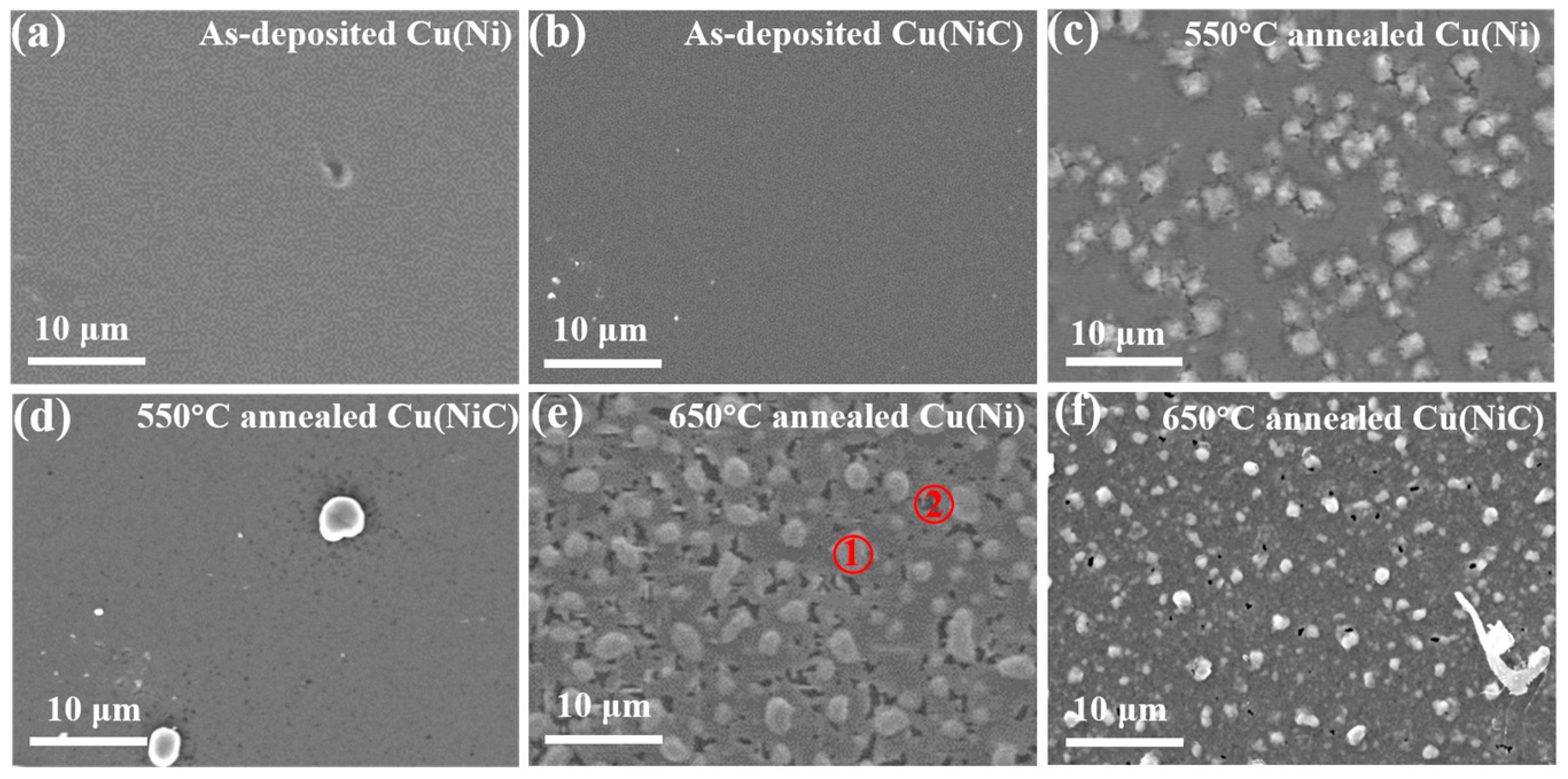
Figure 3 presents the SEM images of the as-deposited and 650 °C annealed Cu(Ni) and Cu(NiC) samples.
Figure 3a,b reveal that the surfaces of as-deposited Cu(Ni) and Cu(NiC) films exhibit a smooth and compact surface without noticeable defects. Defects were identified on the Cu(Ni) sample after annealing at 550 °C, as displayed in
Figure 3c. Defects in the film account for an elevation in sheet resistance in
Figure 2. Cu(NiC) samples exhibit excellent thermal stability as the surface morphology remains unchanged, except for some particles in
Figure 3d. In
Figure 3e, it is evident that with an increase in annealing temperature to 650 °C, the surface of the Cu(Ni) sample exhibits a rough and discontinuous appearance. A multitude of small spherical particles and black holes were observed on the film surface. The brighter particles (area 1) are encircled by darker holes (area 2). From EDS analysis (
Table 1), it can be concluded that the particles are Cu aggregates, and the holes are formed as a result of Cu being lost. The content of carbon is not listed in
Table 1, which is inaccurately measured by the EDS method. Additionally, it was hypothesized that the significant increase in resistance observed in the 650 °C annealed Cu(Ni) film can be attributed to the presence of surface defects. These defects significantly increased the resistance of the Cu(Ni) film and substantially diminished the stability of the Cu(Ni)/Si interconnect structure at 650 °C. The Cu(NiC) samples annealing at 650 °C also displayed the presence of particulate and cavities, as depicted in
Figure 3f. In contrast to the Cu(Ni) samples, there was a significant reduction in both the dimensions and quantity of particulate and cavities. This observation implies that the addition of carbon can greatly improve the surface morphology of the samples annealing at high temperatures. The SEM experiment further demonstrates that the barrier properties of barrierless Cu(Ni) alloy are enhanced significantly after adding C, indicating that the Cu(NiC) barrier layer possesses higher thermodynamic stability than the Cu(Ni) barrier layer.
To accurately analyze the surface distribution of Ni and Si, XPS surface scanning was conducted on 550 °C and 650 °C annealed barrierless Cu(Ni) and Cu(NiC) alloys. By comparing
Figure 4a–d, it is evident that the proportion of Ni element on the surface of the 550 °C annealed Cu(Ni) sample (~9.3%) is higher than that of 550 °C annealed Cu(NiC) (~0.9%). When the annealing temperature was 650 °C, the proportion of Ni element on the surface of the Cu(Ni) sample rose to 12.2%. Nevertheless, the Ni content on the Cu(NiC) surface was only 1.1%. Similarly, the Si element also exhibited a similar trend, as demonstrated in
Figure 4e–h. The proportion of silicon on the surface of the 550 °C annealed Cu(Ni) sample (~1.8%) was greater than that of the Cu(NiC) sample (~0.8%). The silicon content for 650 °C annealed Cu(NiC) samples remained constant. This suggests that the Ni element in the barrierless Cu(Ni) film diffused to the surface of the sample after annealing at 550 °C. In contrast, the barrierless Cu(NiC) film retained its compositional stability even after annealing at 650 °C. Although no distinct peak of copper silicide was observed in the XRD results, the resistance measurements, SEM images, and XPS surface scanning results confirmed that the barrier performance of the Cu(Ni) film started to degrade at 550 °C. Therefore, it can be concluded that the doping of carbon in Cu(Ni) impedes the diffusion of Ni and Si elements, thereby improving the thermal stability of the barrierless film.
The XPS technique was employed to accurately analyze the elemental composition in the surface particles of 650 °C annealed barrierless Cu(Ni) and Cu(NiC) copper alloys.
Figure 5a presents the results of peak fitting analysis for the Ni elements found in the surface particles of the barrierless Cu(Ni) and Cu(NiC) alloy. In the case of Cu(Ni) film, the measurements revealed the peaks at 852.8 eV and 870.0 eV are characteristic of Ni metal [
29], and those at 854.8 eV and 872.1 eV are for the Ni2p3/2 and Ni2p1/2 multiplet-split peaks of NiO [
30]. The satellite peaks of both Ni metal and NiO are indicated by the arrows in
Figure 5a. According to the peak fitting analysis, the surface distribution of Ni elements on the Cu(Ni) copper alloy comprised ~55.8% Ni metal and ~44.2% NiO. After annealing at 650 °C, the Ni elements in the Cu(Ni) copper alloy diffused toward the surface and oxidized due to residual oxygen during vacuum annealing. However, examination of the Ni components in the surface particles of the barrierless Cu(NiC) copper alloy indicated that the particle was composed of Ni metal elements, with no corresponding peak value indicating the presence of NiO components. The peak fitting analysis for the Si components in surface particles of the Cu(Ni) and Cu(NiC) copper alloys is illustrated in
Figure 5b. In the case of the Cu(Ni) film, the peak at 99.6 eV corresponds to the Si element, and the peak at 103.1 eV corresponds to SiO
2, while no peak corresponding to copper silicide was detected [
31,
32]. Similarly, Si atoms diffused toward the surface of the Cu(Ni) film and oxidized in the presence of residual oxygen during vacuum annealing. However, the Cu(NiC) alloy surface exhibited a low Si content, resulting in the absence of XPS peaks. The results indicate that the presence of carbon atoms in Cu(Ni) film effectively hinders the diffusion of Ni and Si atoms toward the surface, thereby enhancing the barrier performance of the barrierless copper alloy.
Figure 6 shows the typical TEM cross-section images of barrierless Cu(Ni) and Cu(NiC) copper alloy after annealing at 650 °C. As shown in
Figure 6a, the Cu(Ni)/Si interconnect interface is readily identifiable. However, the interface is no longer continuous nor intact due to the interdiffusion behavior of Cu and Si atoms. As indicated by the arrows in
Figure 6a, a clear diffusion reaction region is visible at the Cu(Ni)/Si interface. While XRD experiments did not reveal any diffraction peaks, TEM observations indicate that the Cu interface had been disintegrated by atomic diffusion. The appearance of the failure zone suggests that the thermal stability of Cu(Ni) alloy began to degrade. Nevertheless, the Cu(NiC)/Si interface remained flat and undamaged, and no diffusion failure zone was detected. Furthermore, a self-formed layer ~30 nm in width was observed at the interface of Cu(NiC)/Si. The amorphous structure of the self-formed layer, as depicted in the inset Figure in
Figure 6b, serves as an effective barrier against the interdiffusion of Cu and Si atoms. The formation of an amorphous self-formed layer also enhanced the interfacial bonding strength of Cu(NiC)/Si, further improving the high-temperature stability of the barrierless Cu(NiC) copper alloy.
In order to quantitatively analyze the effect of carbon (C) doping on barrierless Cu(Ni) copper alloy films, the diffusion behavior of elements after annealing at 650 °C was investigated by using XPS depth profile analysis.
Figure 7a shows a high O element content on the surface of the Cu(Ni) copper alloy. This was mainly due to the reaction between the residual oxygen present in the chamber and the film, which led to the formation of a significant amount of oxides during the vacuum annealing process. After annealing at 650 °C, the interface between Cu(Ni) and Si lost its distinctness as a result of atom diffusion. This led to a flattened curve for both Cu and Si elements, causing them to overlap across the entire etching area. The observation implies that noticeable atom diffusion occurred in Cu(Ni) film after annealing at 650 °C. The primary reason for the failure of the Cu(Ni) copper alloy film was the diffusion of nickel (Ni) elements to the sample surface. Alloying elements are commonly precipitated at grain boundaries and defects to prevent the interdiffusion of Cu and Si atoms. However, it was evident that the Ni element was absent from the Cu(Ni) film after 500 s of etching, as displayed in
Figure 7a. Thus, the absence of the Ni element cannot impede atom diffusion. A high carbon (C) concentration on the surface of the Cu(NiC) copper alloy was due to surface contamination, as seen in
Figure 7b. Compared with the Cu(Ni) copper alloy, the Cu(NiC) film retained a clear interface. The Cu–Si curves of Cu(NiC) copper alloy displayed a sharp variation exhibiting a distinct Cu/Si interface, revealing the intact interconnect structure of the film. In contrast to the Cu(Ni) copper alloy, the Cu(NiC) copper alloy demonstrated a minimal presence of Ni elements on the surface of the specimen (1.1 at.%). The distribution of nickel within the Cu(NiC) film was consistently around 9%. The Ni elements diminished gradually as they approached the Cu(NiC)/Si interface. Similarly, the distribution of the C element was fairly uniform, at around 5%. During annealing, the doped Ni and C elements precipitated from the copper crystal lattice and gathered at grain boundaries and defects. Consequently, the diffusion path for Cu and Si atoms was blocked by Ni and C elements. Carbon atoms, being smaller in size compared with nickel atoms, have the capability to block smaller diffusion channels among Ni atoms. Hence, the doped C atoms further enhanced the barrier performance of Cu(Ni) film. Additionally, an elevated quantity of O element was observed at the interface of Cu(NiC)/Si, which implies that residual oxygen migrated along the grain boundary to the Cu/Si interface during vacuum annealing. Consequently, a self-formed barrier layer was formed with the Cu(NiC) alloy, as proved by TEM images.
The chemical state of the self-formed layer at the 650 °C annealed Cu(NiC)/Si interface was analyzed using the XPS method. The XPS survey scan shown in
Figure 8a reveals the presence of Cu2p, Ni2p, O1s, and Si2p. The C1s signal was not detected in the XPS survey scan due to its weak intensity. As shown in
Figure 8b, the XPS peak fit of the Cu2p peak revealed a prominent emission of Cu
0 at 932.8 eV and 952.2 eV, accompanied by peaks on the high binding energy (B.E.) side at 933.3 eV and 952.9 eV with weak satellite corresponding to Cu
1+ (Cu
2O) [
33,
34].
Figure 8c shows the C1s spectrum at a B.E. of 284.7 eV, suggesting that the doped C atoms in Cu(NiC) copper alloy are primarily in the C
0 state [
35]. The Si2p peak can be divided into two parts, as displayed in
Figure 8d: the lower B.E. at 99.8 eV for Si
0 and the higher B.E. at 104.0 eV for Si
4+(SiO
2) [
31,
32]. Based on XPS fitting, the Si/SiO
2 ratio was calculated to be 76.7:23.3. In
Figure 8e, the Ni2p XPS spectrum indicates that the predominant components are Ni metal and NiO, with a ratio of approximately 9:1 [
29]. The XPS spectrum depicted in
Figure 8f reveals a B.E. of 530.7 eV, attributed to Cu
2O and NiO, and 533.3 eV associated with SiO
2 [
36,
37]. The XPS analysis of elements in the self-formed barrier layer at the Cu/Si interface indicates that the predominant substance is Cu metal, with the oxides primarily consisting of Cu
2O, NiO, and SiO
2.

 ,
, 


