Article

Enhancement of Photoelectric Performance Based on Ultrathin Wide Spectrum Solar Absorption in Cruciform Microstructure Germanium Solar Cells

1
Hunan Red Solar New Energy Science and Technology Co., Ltd., Changsha 410205, China
2
School of Materials Science and Engineering, Central South University, Changsha 410083, China
3
School of Energy Science and Engineering, Central South University, Changsha 410083, China
*
Author to whom correspondence should be addressed.
Coatings 2023, 13(6), 1123; https://doi.org/10.3390/coatings13061123
Submission received: 22 March 2023 / Revised: 5 June 2023 / Accepted: 12 June 2023 / Published: 19 June 2023
(This article belongs to the Special Issue Micro-Nano Optics and Its Applications)

Abstract

:
In this paper, the solar absorption level of PEDOT:PSS/Ge organic and inorganic hybrid solar cells (HSCs) with different parameters of cruciform microstructure (CM) is studied, using the finite-difference time domain (FDTD) method. The light absorption in HSCs with CM is above 90% in the range of 300 nm to 1300 nm. Under the AM1.5 solar spectrum, the average absorptivity of solar energy is also at a very high level. At the same time, we use DEVICE software to calculate the electrical properties, such as the open-circuit voltage (Voc), short-circuit current density (Jsc), and maximum power density (Pmax). The electrical simulation results show that the Pmax of HSCs with CM improves to 72.16% from the planar HSCs. Besides, in order to study the mechanism of solar energy absorption in HSCs containing CM, the logarithmic plots of electric field intensity of HSCs with CM and planar HSCs, are analyzed at different wavelengths. The work shows that the CM shows an excellent light-trapping effect, which reduces the surface reflectivity of HSCs, and greatly improves the photoelectric conversion efficiency of Ge solar cells.

1. Introduction

Currently, with the consumption of fossil fuels, and environment pollution, energy and the environment have become the focus of society. It is estimated that the global energy consumption will reach 32 terawatts (TW) by 2050 [1]. To solve the energy and environmental crises, improve human living conditions and the quality of human life, and consider the long-term plan of human development, the related research in the field of clean and renewable energy, such as geothermal energy, wind energy, tidal energy, nuclear power, and so on, has gradually attracted a lot of attention [2,3,4,5,6]. Compared to wind energy, hydropower, tidal energy, and geothermal energy as they are currently developed, solar energy is not affected by its geographical location and environment. Thus, solar cells are considered to be the best choice to solve problems such as energy exhaustion and environmental pollution [7,8,9]. Therefore, researchers have invested a lot of research into photovoltaic devices that directly convert solar energy into electricity [10], and people have been pursuing the design of photovoltaic materials and technologies with subwavelength nanostructures [11]. According to current research and development, solar cells are the most widely used technology for solar power generation, which is proved by the strong growth in the number of photovoltaic modules installed. Photovoltaic power generation is expected to account for more than 20% of the world’s primary energy by 2050 [12]. At this stage, it is very necessary to invest a lot of research into solar cells. As we all know, the more light is absorbed, the more electron-hole pairs are created [13]. To date, researchers have used a variety of novel structures and methods, such as using various microstructure to improve solar energy absorption [14]. Among them, low-cost organic hybrid solar cells have shown great potential. Organic solar cells have become a research hotspot because of their light weight, low cost, simple preparation process, good flexibility, and large area preparation [15]. Recently, an efficiency of up to 16% has been reported for the monolayer organic solar cells using non-fullerene receptors [16]. Organic hybrid solar cells have shown great research value and development potential, due to their high efficiency and low cost. A conductive polymer of high conductivity and transparency is needed as the charge transport layer in the study of organic hybrid solar cells. Among many organic materials, poly (3-ethylenedioxythiophene): poly (styrene sulfonic acid) (PEDOT:PSS) has good transparency, adjustable conductivity, and excellent thermal stability, so it is considered to be an ideal organic compound for photovoltaic materials [17]. This material has been used in the research of solar cells [18,19]. The different structures of organic solar cells have a different influence on its performance. The absorption of light, the generation and separation of excitons in the cell, and the transmission of holes and electrons are affected by the different structures of organic solar cells. Therefore, the optimization of the structure can widely enhance the optical performance of organic solar cells. With the development of micro-nano-manufacturing technology, the structure design on the micro-nano scale provides a feasible measure to improve the optoelectronic performance of solar cells [20,21,22]. Surface microstructures can effectively reduce optical loss on the surface of solar cells. Thus, the efficiency of the cells can be improved, which can achieve the purpose of improving the efficiency of solar cells, under the conditions of reducing the use of materials, and reducing production costs [23]. Since the development of related research, a variety of nano-structures have been reported, such as nanopores, nanowires, nanopyramids, and so on [24,25,26,27].
Recently, researchers have conducted a great deal of research on organic solar cells [28,29]. Through various studies, a further understanding has been developed about the relationship between the shape and structure, and the function, of the materials. A lot of research has been conducted on the active layer, to improve the efficiency of organic solar cells. Besides, the absorption distribution and the energy level of the active layer can be adjusted by introducing additional components [30]. Recently, people have improved the efficiency by using a thick active layer containing small molecular donors of liquid crystals, and adjusting the shape of the active layer through hydrogen bonds [31]. However, in order to improve economic competitiveness in the research process, we need to use a thinner active layer, to reduce costs, and to achieve a higher conversion efficiency in the solar cells [32]. Among many materials, Ge is considered to be a very efficient photovoltaic material [33]. Compared with common photovoltaic materials such as silicon and gallium arsenide, the band gap of germanium at room temperature is 0.66 eV, which is significantly smaller than the band gap of the former two at room temperature, which results in the low open-circuit voltage of germanium-based solar cells. The SQ limit of germanium-based solar cells is about 22% [34]. In addition, Ge, a semiconductor material, has a nonlinear absorption coefficient that is inversely proportional to the bandgap energy. Therefore, the absorption coefficient of Ge is higher, and it can increase photoionization in smaller bandgap materials, meaning that Ge is an excellent material as the substrate of solar cells [35].
In this study, the active layer material of the HSCs is germanium (Ge) due to the high absorption coefficient of Ge. PEDOT:PSS as a hole-transport layer has been used in various solar cells. PEDOT:PSS is a kind of aqueous solution of high-molecular polymer, which has a high electrical conductivity. According to different formulations, an aqueous solution with a different electrical conductivity can be obtained. PEDOT:PSS is the most-used high-temperature superconducting material in some solar cells; it can better transport holes to the anode and block electrons, which constitutes a better hole transport layer. PEDOT:PSS can easily form ohmic contact with many common polymers. The absorption coefficient can be further improved by combining Ge with the PEDOT:PSS organic compound. As a result, a higher efficiency can be obtained in the case of using less materials. We use the cruciform microstructure to increase the solar-energy absorption ability. What is more, we study its different geometric parameters in detail. The solar energy absorption curves of the HSCs with CM, and the planar HSCs, are plotted, respectively. Furthermore, the light absorption among different heights and widths of CM are obtained. At the same time, the electrical properties are calculated using DEVICE software under the condition of different geometric parameters of CM, and we get different Jsc, Voc, and Pmax of the HSCs. In addition, the logarithmic plots of electric field intensity of the HSCs with CM, and the planar HSCs, are also investigated at different wavelengths. Through further exploration in the future, it is believed that this work could have a good role to play in promoting improvement in the performance of Ge HSCs.

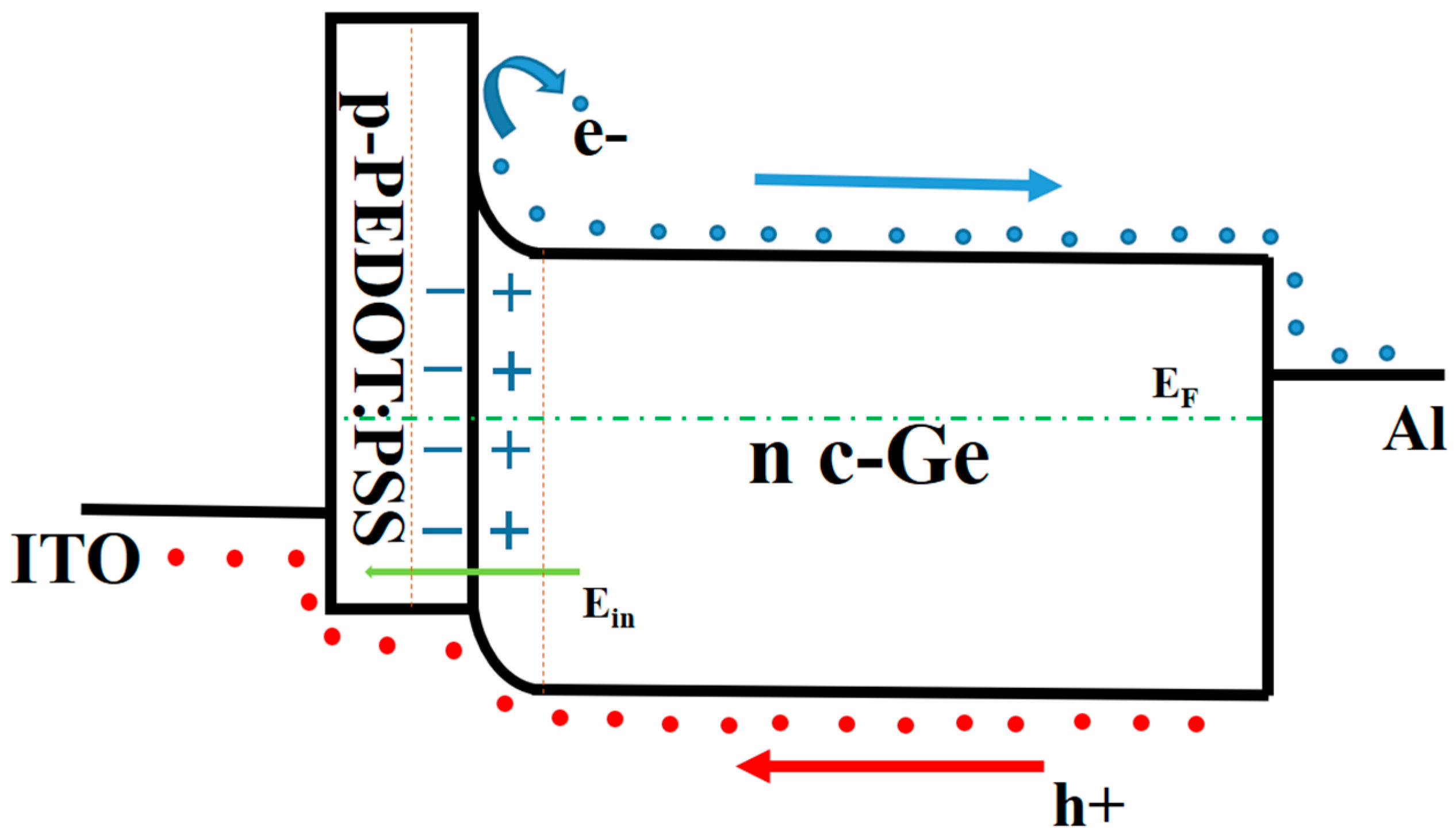
2. Structure and Method

In the process of this research, we use FDTD and DEVICE software (version) for modeling and simulation. Within current research and development, there are many methods for the calculation and analysis of electromagnetic fields, such as the finite element method, equivalent source method, moment method, and so on [36,37,38,39]. Our use of the FDTD method is based on the vector three-dimensional Maxwell equation, using FDTD to optimize the spatial grid, and obtain the corresponding results from the time-domain signal. This method for analyzing the electromagnetic field of solar cells is the most widely used and effective method. FDTD can directly discretize the time-domain wave equation, and its difference scheme contains the parameters of the medium, as long as the corresponding parameters are given to each grid, so that various complex structures can be simulated [40,41,42].
Figure 1a is a 3D view of the overall structure of the HSCs. At the bottom is the aluminum (Al) layer, which acts as an electrode. The Ge overlaps above the Al layer, and is the main active layer of the HSCs. The cruciform microstructure of Ge is located in the central position of a periodic simulation unit. The CM microstructure proposed in this paper is mainly completed through template lithography, development, etching, cleaning, and other steps. The exposure time mainly depends on the thickness of the photoresist, and the etching time is mainly determined by the etching depth. The presence of the CM microstructure increases the scattering and multiple reflection probability of incident light, increasing the optical path of incident light propagation in the photoactive layer, and reducing the reflectivity of incident light, thereby increasing the photoelectric conversion efficiency of the HSCs. The photoelectric conversion performance of the HSCs can be effectively improved due to the light-capturing characteristics of the cruciform microstructure. The conformal coating above the CM is P-type PEDOT:PSS, which plays the role of the hole-transport layer and electron-block layer. Above the organic layer is the transparent conductive film (ITO), which plays a role as a photogenerated hole-collection electrode. In addition, we place an optical flat quartz substrate, with good light transmittance, on the top of the whole structure, to focus incident sunlight [43,44,45,46]. Figure 1b,c show the top view and section view of the entire structure, respectively. We set the optimal geometric parameters of each part of the structure through simulation. In Figure 1b, P and W represent the period of a simulation unit of, and the width of, the cruciform microstructure, respectively. As shown in Figure 1c, the optimal thickness of the glass, ITO, PEDOT:PSS, Ge, and Al is a = 100 nm, b = 80 nm, c = 500 nm, d = 900 nm, and e = 200 nm, from top to bottom. The length of the cruciform microstructure is represented by L = 200 nm, and the height of the cruciform microstructure is represented by h. All the above parameters are optimized based on the FDTD software. As shown in Figure 2, n-type Ge and p-type PEDOT:PSS combine to form a PN junction and a unified Fermi level (EF). At the same time, the built-in electric field (Ein) is formed, and the direction of electric field is from N-type germanium to P-type PEDOT:PSS. Therefore, electrons are blocked by PEDOT:PSS, and transported to the Al electrode. Holes are effectively transported through PEDOT: PPS, and collected through the ITO.
Here, we use plane waves, with wavelengths in the range of 300 nm to 1500 nm, to incident to the surface of the HSCs, along the negative direction of the Z-axis. In the X-axis and Y-axis directions, we use periodic boundary conditions. In the Z-axis direction, we use the perfectly matched layer (PML) boundary condition, to avoid parasitic reflection and electromagnetic absorption. FDTD can calculate the light power absorbed per unit volume that can be expressed in the following formula [47]:
P a b s = 0.5 ω | E | 2 I m { ε }
where ω is the frequency of the electromagnetic wave, E is the electric field, ε is the dielectric constant, and Im{ε} is the imaginary part of the dielectric constant. Under the condition of the AM1.5 solar spectrum, the important parameter used to describe the solar cells, namely the short-circuit current density, under the assumption that each photon absorbed by the active layer will produce a photogenerated electron–hole pair, the ideal Jsc value can be calculated using the following formula [48]:
J s c = q 2 π c 300   n m 1500   n m λ Q E ( λ ) I A M 1.5 λ d λ
where q is the charge of the electron, λ is the wavelength possessed by the light source, c is the propagation speed of light in vacuum, the quantum efficiency of the solar cells is the QE(λ) in the formula, and the irradiance of sunlight under the AM1.5 solar spectrum is expressed by IAM1.5. The following formula can express the number of photogenerated carriers per unit volume [49]:
G = P a b s ω = 0.5 I m ε
where ħ is the reduced Planck constant, and the corresponding frequency of the energy of a photon is 2 π ω. The total luminous yield is the integral of G in the whole range, which is related to frequency and space. Based on the relevant physical theory expressed by formulas (1)–(3), we can calculate the light production rate using the FDTD software, and then input it into the DEVICE software for electrical simulation. With the support of semiconductor physics theory, we can obtain the Jsc, Voc, Pmax, and other photovoltaic parameters of the HSCs under different geometric parameters.

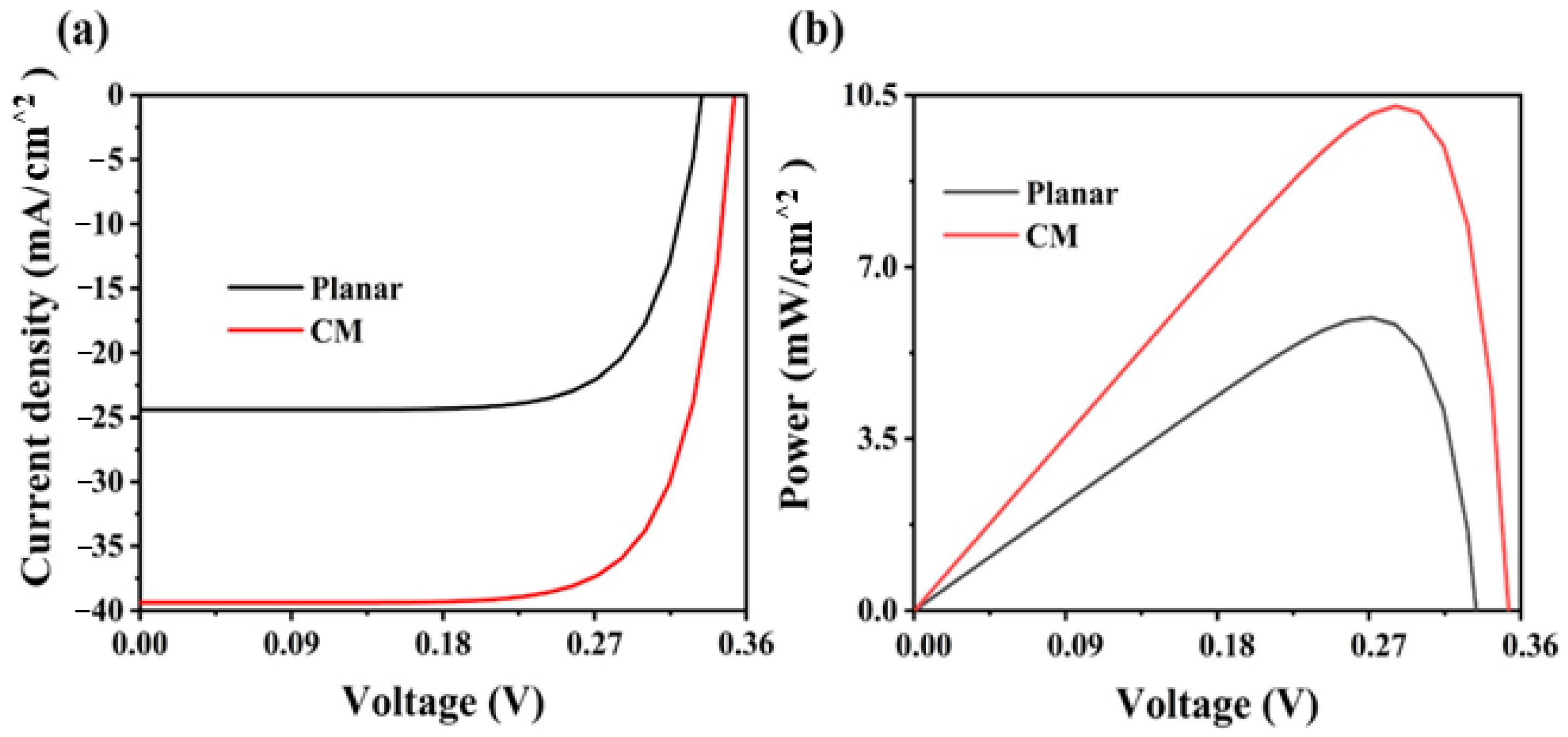
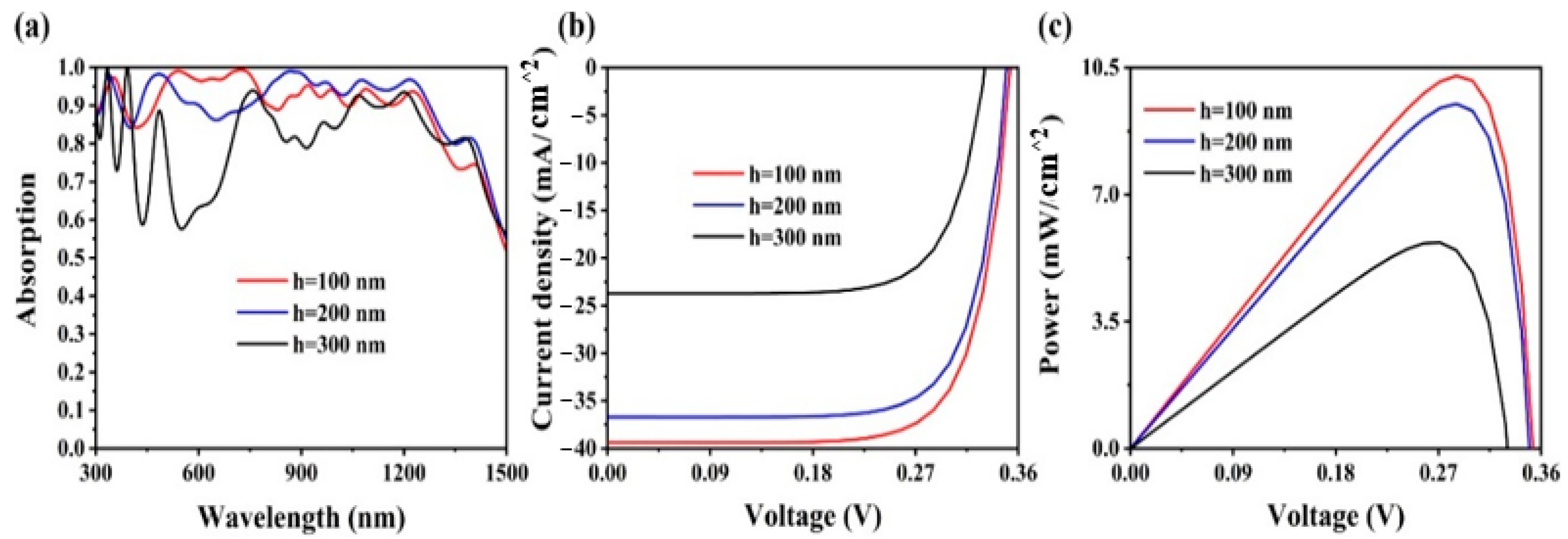
3. Simulation Results and Discussion

We have fully studied the optical properties of the HSCs with the CM, and the planar HSCs. We calculated the reflection (R) and absorption (A) spectra of these two different structures. In Figure 3a, the light absorption rate in the HSCs with CM is basically higher than 90% in the light wavelength range of 300 nm to 1300 nm. The dynamic dielectric constant of the germanium from 400 nm to 700 nm determines its high reflectivity in this range, while solar cells with CM adjust the distribution of the dielectric constant, due to the presence of microstructures, thereby adjusting the absorption performance of the solar cells. With the changing of the wavelength, the absorption curve of the HSCs with CM only fluctuates within a small range, while the absorption in the planar HSCs fluctuates over a large range at a level below 90%. In Figure 3b, it can be seen that the convex surface of the CM has a significant effect on suppressing the reflection. Comparing the two figures, we can find that a very key factor affecting light absorption is reflection. For example, at the light wavelength of 500 nm, the light absorption in the planar HSCs is relatively small, because the reflection level of the planar HSCs at 500 nm is higher.
We further study the response of the HSCs under the AM1.5 solar spectrum, to simulate the optical absorption performance under sunlight. The responses of the HSCs with the CM, and the planar HSCs, under the AM1.5 solar spectrum, were compared. The comparison results for the light absorption efficiency are shown in Figure 4. In Figure 4a, the average absorption rate of the planar HSCs is not very high in the entire wavelength range (300–1500 nm), especially in the wavelength range of 500–900 nm, in which the absorption performance is relatively poor. As shown in Figure 4b, in the entire wavelength range (300–1500 nm), the average absorption rate of the HSCs with CM is very high. Obviously, compared with the planar HSCs, the absorption performance of the HSCs with CM has been greatly improved.
In order to achieve a more detailed description of the relationship between light absorption and various incident angles [50,51,52,53], we studied the relationship between the different incident angles of planar light (0°, 20°, 40°, and 60°), and light absorption in the HSCs with CM. As shown in Figure 5a, it can be observed that the incident angle is negatively correlated with the light absorption. As the angle increases, the light absorption rate shows a decline trend, but the overall absorption level has basically remained above 70%. It can be seen that the influence of light from different directions on light absorption in the HSCs with CM is not very significant, and the small angle change has a very small effect on the light absorption. This indicates that the HSCs with CM have a very good light absorption performance under actual sunlight. Besides, it can be seen that, except for the black curve (60°) with the relatively different trend, the trends of the curves corresponding to three different angles (0°, 20°, and 40°) are basically the same from 600 nm to 900 nm. In Figure 5b, the relationship between the angle, and the electric field intensity and the light absorption, can be seen more intuitively. It is found that around 170 nm, around 420 nm, between 700 nm and 800 nm, and between 1020 nm and 1150 nm, the light absorption declines with the increase in the angle. On the whole, as the angle changes, we see that the larger the angle, the smaller the light absorption.
We use the DEVICE software to simulate several different geometric parameters, selected from the optical simulation, to better show the optimal characteristics of the geometric parameters of the HSCs. In Figure 6a, the Voc of the planar HSCs achieves 0.33 V, and the Jsc is about 24.41 mA/cm2. The Voc and the Jsc of the HSCs with CM are approximately 0.35 V and 39.39 mA/cm2, respectively. The presence of the CM microstructure regulates the distribution of the dielectric constant, and increases the multiple reflection probability of incident light, increasing the optical path of incident light propagation in the photoactive layer, and reducing the reflection of incident light, thereby increasing the short-circuit current density, and the power density of the cells. The results of this study show that the Voc and Jsc of the HSCs have been improved to a certain extent after adopting the CM. The maximum power density (Pmax) of the planar HSCs, and the maximum power density of the HSCs with CM, are shown in Figure 6b, which are 5.97 mW/cm2 and 10.27 mW/cm2, respectively. The Pmax of the HSCs with CM is more than 1.7 times that of the planar HSCs. The results show that the CM has greatly improved the Pmax of the HSCs, due to the improvement of the Voc and the Jsc.
We compare and analyze the logarithmic figure of the HSCs with CM, and the planar HSCs with different wavelengths. Figure 7a–f, respectively, show the distribution of the electric field intensity of the planar HSCs and the HSCs with CM under three different wavelength conditions of 350 nm, 600 nm, and 1200 nm, respectively. As shown in Figure 7a,d, when the wavelength is 350 nm, the PEDOT:PSS layer limits most of the electric field of the planar HSCs, then the interference of the electric field intensity distribution occurs in the PEDOT:PSS layer [54,55]. The maximum energy of shortwave can be seen from the absence of high electric field in the Ge substrate; that it is confined to the PEDOT:PSS layer. For the HSCs with CM, the diffraction distribution of the electric field still occurs, and the high electric field is also distributed on both sides of the CM. The electric field intensity of the Ge cruciform microstructure is slightly higher than that of the Ge substrate. We can see from Figure 7b,e, when λ = 600 nm, the electric field distribution of the planar HSCs is similar to that in Figure 7a, but the width of the interference fringes becomes wider. In addition, the intensity of the electric field located at the top of the Ge substrate is also enhanced. For the HSCs with CM, the higher electric field intensity is uniformly distributed in the region above the cruciform microstructure. The highest electric field intensity is distributed on both sides of the cruciform microstructure. Comparing Figure 7e with Figure 7d, the electric field intensity distribution in the area above the cruciform microstructure of Figure 7e becomes more uniform. In addition, the electric field intensity further diffuses into the interior of the cruciform microstructure. This is consistent with the high absorption result at 600 nm in Figure 7a. The absorption ability of solar energy, and the number of electron-hole pairs, may be increased due to optical coupling under the condition of a high electric field [56,57,58]. As shown in Figure 7c,f, when λ = 1200 nm, the width of the interference fringes of the planar HSCs is further broadened as the wavelength increases. Moreover, the phenomenon of additional interference patterns also occurs in the Ge substrate. The results show that the long-wave energy diffuses down to the Ge substrate. For the HSCs with CM, it can be observed that the electric field begins to shift gradually to the bottom of the cruciform microstructure with the redshift in the wavelength. The electric field intensity distribution above the cruciform microstructure is more uniform than that in Figure 7e, and the electric field intensity is slightly increased, and additional interference fringes also appear in the entire Ge substrate. In short, the cruciform microstructure plays a good role in regulating the light coupling, and performs very well light-trapping, in the absorption of solar energy.
Figure 8a shows the light absorption curve corresponding to each wavelength when the thicknesses of Ge are 400 nm, 500 nm, 600 nm, 700 nm, 800 nm, 900 nm and 1000 nm respectively. The results show that in the wavelength range of 300–750 nm, except for the black curve, the other curves almost overlap. There are some continuous fluctuations from 750 nm to 1500 nm, but the trend of each curve is basically the same, indicating that the effect of the Ge thickness on optical absorption is not very significant in this wavelength range. The overall absorption level from 300 nm to 1200 nm is basically more than 80%, maintaining a relatively stable trend as a whole. In the long-band range of 1200~1500 nm, because the reflection in this region increases with the wavelength, the absorption level of solar energy decreases gradually with the increase in wavelength, but the lowest level is maintained at about 60%. The curves crisscross and overlap, and the change in the thickness of Ge has no obvious effect on the optical absorption when the wavelength is greater than 400 nm. Figure 8b shows the J–V curve of the Ge thicknesses at 400 nm, 500 nm, 600 nm, 700 nm, 800 nm, 900 nm, and 1000 nm, respectively. From the figure, we can see that the light absorption among the different active layer thicknesses is not significantly different. However, the thinner their thickness, the higher the recombination rate of their charge carriers. Therefore, through electrical simulation, we chose the optimal thickness of 900 nm. The results show that as the thickness increases, Jsc gradually decreases. However, after about 0.27 V, cross-changes begin to appear between the curves. The corresponding Voc between each curve is between 0.34 V and 0.36 V. The thickness of the Ge has little effect on the short-circuit current density and open-circuit voltage of the HSCs. Figure 8c shows the P–V curves of the Ge thicknesses at 400 nm, 500 nm, 600 nm, 700 nm, 800 nm, 900 nm, and 1000 nm, respectively. As can be seen from the figure, the difference between the curves is very small, and basically consistent. On the whole, with the increase in the thickness of the Ge, the maximum power density increases slightly.
Figure 9a shows the absorption curves for the different heights of the CM. It can be seen from this figure that the trend in the three curves from 1050 nm to 1500 nm is basically the same, and the absorption decreases gradually with the increase in wavelength. The height of the CM has no significant effect on the absorption, but the peak value of the wave shifts slightly to the left with the increase in the height of the CM [59,60]. The black curve fluctuates greatly from 300 nm to 1050 nm, the blue and red curves are relatively stable and compact, and the absorption is more than 85%. Figure 9b shows J–V curves of different heights. It can be seen from this figure that when the height of the CM is 100 nm, the Jsc is 39.39 mA/cm2. The lowest Jsc is obtained when the height of the CM is 300 nm, which is 23.75 mA/cm2. The height of the CM has a very obvious effect on the short-circuit current density of the HSCs. With the increase in CM height, the short-circuit current density of the HSCs decreases significantly. Similarly, we can also see that the Voc of HSCs is slightly higher than that of 100 nm when the height is 200 nm. With the increase in height, the Voc of each curve decreases gradually. This shows that there is an inverse relationship between the Voc of HSCs, and the height of CM. Figure 9c shows the P–V curve of the CM at different heights. It can be seen from this figure that it corresponds to the result of the J–V curve. When the height of the HSCs is 100 nm, the Pmax is 10.27 mW/cm2. When the height is 300 nm, Pmax is the lowest at 5.97 mW/cm2. The higher the height of the CM, the lower the Pmax.
Figure 10a shows the absorption curves of the different widths of CM. It can be seen from the figure that from 900 nm to 1500 nm, except for the black curve, the trends in the other three curves are basically the same, and from 1050 nm to 1500 nm, the three curves almost overlap. From 300 nm to 900 nm, the black curve fluctuates greatly, and the other three curves are relatively stable, and the absorption rate is above 80%. In the wavelength range of 300~1200 nm, the curve fluctuates continuously, and with the decrease in the width of the cruciform microstructure, the peak shifts slightly to the right. In Figure 10b, the J–V curve is shown at the different widths of CM. It can be seen from this figure that the Jsc of the different heights is between 37.5 mA/cm2 and 40 mA/cm2. The corresponding Voc between each curve is between 0.34 V to 0.36 V; the difference is very small. The width of the CM has little effect on the Jsc and Voc of the HSCs. The P–V curves of different widths are shown in Figure 10c. It can be seen from this figure that it corresponds to the result of the J–V curve. The Pmax corresponding to each width is between 9.63 mW/cm2 and 10.15 mW/cm2. The change in the width of the CM is not an important factor affecting Pmax. From Table 1, we can see that our work has significantly improved efficiency, while reducing the thickness of the solar active layer, compared to previous works.

4. Conclusions

We use the FDTD software to simulate the HSCs that we design, and theoretically analyze the optical and electrical characteristics of the HSCs with or without CM. The absorption of sunlight is the crux of solar cells, and the basis of the energy conversion of solar cells. The results show that absorption in the HSCs with CM is more than 90% in the range of 300~1300 nm. The electric field intensity analysis shows that the light-capturing ability of the HSCs with CM becomes stronger. Moreover, the maximum Jsc of the HSCs with CM, calculated by the DEVICE software, is 39.39 mA/cm2, which is much higher than the Jsc of the planar HSCs. In addition, we also compare the results of optical absorption, Jsc, Voc, and Pmax under the condition of different heights and widths of CM. We believe that our research has some theoretical significance to the design of HSCs. Our research could further promote the research and development of hybrid solar cells, and further improve the conversion efficiency of Ge HSCs.

Author Contributions

Conceptualization, Z.Z. and W.L.; data curation, Z.Z. and H.H.; formal analysis, Z.Z. and X.D.; methodology, Z.Z., W.L. and X.D.; resources, X.L.; software, Z.Z., W.L., H.H. and X.D.; data curation, Z.Z.; writing—original draft preparation, Z.Z.; writing—review and editing, Z.Z., W.L., H.H. and X.D. All authors have read and agreed to the published version of the manuscript.

Funding

The authors are grateful for the support from the Scientific Research Fund of Zhejiang Provincial Education Department (Y202146019).

Institutional Review Board Statement

Not applicable.

Informed Consent Statement

Not applicable.

Data Availability Statement

Publicly available datasets were analyzed in this study. This data can be found here: https://www.lumerical.com/ (accessed on 1 January 2020).

Conflicts of Interest

The authors declare no conflict of interest.

References

  1. Wang, Z.; Liu, Y.; Li, L.; Gao, S.; Zhu, D.; Yu, X.; Cheng, S.; Zheng, D.; Xiong, Y. An investigation of the effects of ZnO inverse opal pore size in the composite of ZnO nanorods/ZnO inverse opal on the performance of quantum dot-sensitized solar cells. Dalton Trans. 2023, 52, 81–89. [Google Scholar] [CrossRef] [PubMed]
  2. Wu, X.; Yin, C.; Zhang, M.; Xie, Y.; Hu, J.; Long, R.; Wu, X.; Wu, X. The Intercalation Cathode of MOFs-driven Vanadium-based Composite Embedded in N-doped Carbon for Aqueous Zinc ion Batteries. Chem. Eng. J. 2023, 452, 139573. [Google Scholar] [CrossRef]
  3. Meng, W.; Li, C.; Yao, M.; He, Z.; Wu, X.; Jiang, Z.; Dai, L.; Wang, L. Synthesis and electrochemical performance of Li1+xTi2−xFex(PO4)3/C anode for aqueous lithium ion battery. Adv. Powder Technol. 2020, 31, 1359–1364. [Google Scholar] [CrossRef]
  4. Zhao, F.; Lin, J.; Lei, Z.; Yi, Z.; Qin, F.; Zhang, J.; Liu, L.; Wu, X.; Yang, W.; Wu, P. Realization of 18.97% theoretical efficiency of 0.9 µm Thick c-Si/ZnO Heterojunction Ultrathin-film Solar Cells via Surface Plasmon Resonance Enhancement. Phys. Chem. Chem. Phys. 2022, 24, 4871–4880. [Google Scholar] [CrossRef] [PubMed]
  5. Wu, X.; Li, Y.; Xiang, Y.; Liu, Z.; He, Z.; Wu, X.; Li, Y.; Xiong, L.; Li, C.; Chen, J. Mixed-valence cobalt oxides bifunctional electrocatalyst with rich oxygen vacancies for aqueous metal-air batteries. Chem. Eng. J. 2023, 453, 139831. [Google Scholar] [CrossRef]
  6. Tang, F.; Wu, X.; Shen, Y.; Xiang, Y.; Wu, X.; Xiong, L.; Wu, X. The intercalation cathode materials of heterostructure MnS/MnO with dual ions defect embedded in N-doped carbon fibers for aqueous zinc ion batteries. Energy Storage Mater. 2022, 52, 180–188. [Google Scholar] [CrossRef]
  7. Sivaram, P.M.; Mande, A.B.; Premalatha, M.; Arunagiri, A. Investigation on a building-integrated passive solar energy technology for air ventilation, clean water and power. Energy Convers. Manag. 2020, 211, 112739. [Google Scholar] [CrossRef]
  8. Wu, F.Y.; Shi, P.C.; Yi, Z.; Li, H.L.; Yi, Y.G. Ultra-Broadband Solar Absorber and High-Efficiency Thermal Emitter from UV to Mid-Infrared Spectrum. Micromachines 2023, 14, 985. [Google Scholar] [CrossRef]
  9. Liu, Y.; Wang, Z.; Li, L.; Gao, S.; Zheng, D.; Yu, X.; Wu, Q.; Yang, Q.; Zhu, D.; Yang, W.; et al. Highly efficient quantum-dot-sensitized solar cells with composite semiconductor of ZnO nanorod and oxide inverse opal in photoanode. Electrochim. Acta 2022, 412, 140145. [Google Scholar] [CrossRef]
  10. Ren, Y.; Zhou, T.; Jiang, C.; Tang, B. Thermally switching between perfect absorber and asymmetric transmission in vanadium dioxide-assisted metamaterials. Opt. Express 2021, 29, 7666–7679. [Google Scholar] [CrossRef]
  11. Zhu, Y.; Tang, B.; Yang, N.; Lang, X.; Su, J.; Li, Z. Tunable wide-angle perfect absorber based on black phosphorous-dielectric-metallic hybrid architecture. Phys. E 2021, 126, 114449. [Google Scholar] [CrossRef]
  12. Kunta, Y.; Hayato, K.; Wataru, Y.; Toru, I.; Katsunori, K.; Kunihiro, N.; Toshihiko, U.; Daisuke, A.; Masanori, K.; Hisashi, U.; et al. Silicon heterojunction solar cell with interdigitated back contacts for a photoconversion efficiency over 26%. Nat. Energy 2017, 2, 17032. [Google Scholar]
  13. Lai, R.; Shi, P.; Yi, Z.; Li, H.; Yi, Y. Triple-Band Surface Plasmon Resonance Metamaterial Absorber Based on Open-Ended Prohibited Sign Type Monolayer Graphene. Micromachines 2023, 14, 953. [Google Scholar] [CrossRef] [PubMed]
  14. Li, W.; Ma, J.; Zhang, H.; Cheng, S.; Yang, W.; Yi, Z.; Yang, H.; Zhang, J.; Wu, X.; Wu, P. Tunable broadband absorber based on a layered resonant structure with a Dirac semimetal. Phys. Chem. Chem. Phys. 2023, 25, 8489–8496. [Google Scholar] [CrossRef] [PubMed]
  15. Zhang, Y.; Yi, Y.; Li, W.; Liang, S.; Ma, J.; Cheng, S.; Yang, W.; Yi, Y. High Absorptivity and Ultra-Wideband Solar Absorber Based on Ti-Al2O3 Cross Elliptical Disk Arrays. Coatings 2023, 13, 531. [Google Scholar] [CrossRef]
  16. Zhu, L.; Zhang, M.; Zhou, G.Q.; Hao, T.Y.; Xu, J.Q.; Wang, J.; Qiu, C.Q.; Prine, N.; Ali, J.; Feng, W.; et al. Efficient Organic Solar Cell with 16.88% Efficiency Enabled by Refined Acceptor Crystallization and Morphology with Improved Charge Transfer and Transport Properties. Adv. Energy Mater. 2020, 10, 1904234. [Google Scholar] [CrossRef]
  17. Zeng, M.; Wang, X.J.; Ma, R.J.; Zhu, W.Y.; Li, Y.; Chen, Z.X.; Zhou, J.W.; Li, W.Q.; Liu, T.; He, Z.C.; et al. Dopamine Semiquinone Radical Doped PEDOT:PSS: Enhanced Conductivity, Work Function and Performance in Organic Solar Cells. Adv. Energy Mater. 2020, 10, 2000743. [Google Scholar] [CrossRef]
  18. Bipanko, K.M.; Shaikh, K.M.; Rashid, M.A.; Abdul, K.; Hajime, S.; Jaker, H. Effect of CdS and In3Se4 BSF layers on the photovoltaic performance of PEDOT:PSS/n-Si solar cells: Simulation based on experimental data. Superlattices Microstruct. 2021, 152, 106853. [Google Scholar]
  19. Dilpreet, S.M.; You-Hyun, S.; Kwon, S.N.; Na, S.I. Efficient and stable planar perovskite solar cells with a PEDOT:PSS/SrGO hole interfacial layer. J. Alloys Compd. 2020, 812, 152091. [Google Scholar]
  20. Liang, S.; Xu, F.; Yang, H.; Cheng, S.; Yang, W.; Yi, Z.; Song, Q.; Wu, P.; Chen, J.; Tang, C. Ultra long infrared metamaterial absorber with high absorption and broad band based on nano cross surrounding. Opt. Laser Technol. 2023, 158, 108789. [Google Scholar] [CrossRef]
  21. Tang, B.; Yang, N.; Huang, L.; Su, J.; Jiang, C. Tunable anisotropic perfect enhancement absorption in black phosphorus-based metasurfaces. IEEE Photonics J. 2020, 12, 4500209. [Google Scholar] [CrossRef]
  22. Li, J.; Liu, G.; Liu, B.; Min, Z.; Qian, D.; Jiang, J.; Li, J. An extremely facile route to Co2P encased in N,P-codoped carbon layers: Highly efficient bifunctional electrocatalysts for ORR and OER. Int. J. Hydrogen Energy 2018, 43, 77. [Google Scholar] [CrossRef]
  23. Zhao, F.; Chen, X.F.; Yi, Z.; Qin, F.; Tang, Y.J.; Yao, W.T.; Zhou, Z.G.; Yi, Y.G. Study on the solar energy absorption of hybrid solar cells with trapezoidpyramidal structure based PEDOT:PSS/c-Ge. Sol. Energy 2020, 204, 635–643. [Google Scholar] [CrossRef]
  24. Shan, L.; Zhou, J.; Zhang, W.; Xia, C.; Guo, S.; Ma, X.; Fang, G.; Wu, X.; Liang, S. Highly Reversible Phase Transition Endows V6O13 with Enhanced Performance as Aqueous Zinc-Ion Battery Cathode. Energy Technol. 2019, 7, 57. [Google Scholar] [CrossRef]
  25. Zhu, Y.; Tang, B.; Jiang, C. Tunable broadband bandwidth anisotropic absorber based on multi-layer black phosphorus ribbons. Appl. Phys. Express 2019, 12, 032009. [Google Scholar] [CrossRef]
  26. Pushpa, R.P.; Francisco, R.Z.; Manisha, S.; David, E.; Arturo, P.; Arturo, A.A. High Efficiency Hybrid Silicon Nanopillar–Polymer Solar Cells. ACS Appl. Mater. Interfaces 2013, 5, 9620–9627. [Google Scholar]
  27. Wu, X.; Li, Y.; Li, C.; He, Z.; Xiang, Y.; Xiong, L.; Chen, D.; Yu, Y.; Sun, K.; He, Z.; et al. The electrochemical performance improvement of LiMn2O4/Zn based on zinc foil as the current collector and thiourea as an electrolyte additive. J. Power Sources 2015, 300, 453–459. [Google Scholar] [CrossRef]
  28. Chen, Y.C.; Hsu, C.Y.; Lin, R.Y.; Ho, K.C.; Lin, J.T. Materials for the Active Layer of Organic Photovoltaics: Ternary Solar Cell Approach. ChemSusChem 2013, 6, 20–35. [Google Scholar] [CrossRef]
  29. Chen, Z.H.; Cai, P.G.; Wen, Q.Y.; Chen, H.; Tang, Y.J.; Yi, Z.; Wei, K.H.; Li, G.F.; Tang, B.; Yi, Y.G. Graphene Multi-Frequency Broadband and Ultra-Broadband Terahertz Absorber Based on Surface Plasmon Resonance. Electronics 2023, 12, 2655. [Google Scholar] [CrossRef]
  30. Li, C.; Shi, X.; Liang, S.; Ma, X.; Han, M.; Wu, X.; Zhou, J. Spatially homogeneous copper foam as surface dendrite-free host for zinc metal anode. Chem. Eng. J. 2020, 379, 122248. [Google Scholar] [CrossRef]
  31. Noh, J.H.; Im, S.H.; Heo, J.H.; Mandal, T.N. Chemical Management for Colorful, Efficient, and Stable Inorganic−Organic Hybrid Nanostructured Solar Cells. Nano Lett. 2013, 13, 1764–1769. [Google Scholar] [CrossRef] [PubMed]
  32. Mikio, T.; Ayumu, Y.; Satoshi, T.; Kenta, M.; Yuya, N.; Takeshi, N.; Kazunori, F.; Eiji, M. 24.7% Record Efficiency HIT Solar Cell on Thin Silicon Wafer. IEEE J. Photovolt. 2013, 4, 96–99. [Google Scholar]
  33. Alcañiz, A.; López, G.; Martín, I.; Jiménez, A.; Datas, A.; Calle, E.; Ros, E.; Gerling, L.G.; Voz, C.; Cañizo, C.; et al. Germanium photovoltaic cells with MoOx hole-selective contacts. Sol. Energy 2019, 181, 357–360. [Google Scholar] [CrossRef] [Green Version]
  34. Ten-Kate, O.M.; De-Jong, M.; Hintzen, H.T.; Van-Der-Kolk, E. Efficiency enhancement calculations of state-of-the-art solar cells by luminescent layers with spectral shifting, quantum cutting, and quantum tripling function. J. Appl. Phys. 2013, 114, 084502. [Google Scholar] [CrossRef] [Green Version]
  35. Daniel, M.; Jeremy, P.; Sergei, T.; Ilan, B.Z.; Chan, J. Measurements of nonlinear absorption of intense 10 µm laser pulses in n-Ge, GaAs, and ZnSe. Appl. Opt. 2020, 59, 7912–7917. [Google Scholar]
  36. Ye, Z.; Wu, P.; Wang, H.; Jiang, S.; Huang, M.; Lei, D.; Wu, F. Multimode tunable terahertz absorber based on a quarter graphene disk structure. Results Phys. 2023, 48, 106420. [Google Scholar] [CrossRef]
  37. Zhu, W.; Yi, Y.; Yi, Z.; Bian, L.; Yang, H.; Zhang, J.; Yu, Y.; Liu, C.; Li, G.; Wu, X. High confidence plasmonic sensor based on photonic crystal fiber with U-shaped detection channel. Phys. Chem. Chem. Phys. 2023, 25, 8583. [Google Scholar] [CrossRef]
  38. Tang, B.; Ren, Y. Tunable and switchable multi-functional terahertz metamaterials based on a hybrid vanadium dioxide–graphene integrated configuration. Phys. Chem. Chem. Phys. 2022, 24, 8408–8414. [Google Scholar] [CrossRef]
  39. Qi, H.; Tang, B. An active tunable terahertz functional metamaterial based on hybrid-graphene vanadium dioxide. Phys. Chem. Chem. Phys. 2023, 25, 7825–7831. [Google Scholar] [CrossRef]
  40. Li, W.; Yi, Y.; Yang, H.; Cheng, S.; Yang, W.X.; Zhang, H.; Yi, Z.; Yi, Y.; Li, H. Active Tunable Terahertz Bandwidth Absorber Based on single layer Graphene. Commun. Theor. Phys. 2023, 75, 045503. [Google Scholar] [CrossRef]
  41. Zheng, Y.; Yi, Z.; Liu, L.; Wu, X.W.; Liu, H.; Li, G.F.; Zeng, L.C.; Li, H.L.; Wu, P.H. Numerical simulation of efficient solar absorbers and thermal emitters based on multilayer nanodisk arrays. Appl. Therm. Eng. 2023, 230, 120841. [Google Scholar] [CrossRef]
  42. Tang, B.; Li, Z.; Palacios, E.; Liu, Z.; Butun, S.; Aydin, K. Chiral-Selective Plasmonic Metasurface Absorbers Operating at Visible Frequencies. IEEE Photonics Technol. Lett. 2017, 29, 295–298. [Google Scholar] [CrossRef]
  43. Li, Y.; Yang, S.; Du, H.; Liu, Y.; Wu, X.; Yin, C.; Wang, D.; Wu, X.; He, Z.; Wu, X. A stable fluoride-based interphase for a long cycle Zn metal anode in an aqueous zinc ion battery. J. Mater. Chem. A 2022, 10, 14399–14410. [Google Scholar] [CrossRef]
  44. Chen, H.; Li, W.; Zhu, S.M.; Hou, A.Q.; Liu, T.; Xu, J.S.; Zhang, X.W.; Yi, Z.; Yi, Y.G.; Dai, B. Study on the Thermal Distribution Characteristics of a Molten Quartz Ceramic Surface under Quartz Lamp Radiation. Micromachines 2023, 14, 1231. [Google Scholar] [CrossRef]
  45. Chen, H.; Chen, Z.H.; Yang, H.; Wen, L.H.; Yi, Z.; Zhou, Z.G.; Dai, B.; Zhang, J.G.; Wu, X.W.; Wu, P.H. Multi-mode surface plasmon resonance absorber based on dart-type single-layer graphene. RSC Adv. 2022, 12, 7821–7829. [Google Scholar] [CrossRef]
  46. Ren, Y.; Tang, B. Switchable Multi-Functional VO2-Integrated Metamaterial Devices in the Terahertz Region. J. Light. Technol. 2021, 39, 5864–5868. [Google Scholar] [CrossRef]
  47. Zhu, L.; Hu, R.; Xiang, Y.; Yang, X.; Chen, Z.; Xiong, L.; Wu, X.; He, Z.; Lei, W. Enhanced performance of Li-S battery by constructing inner conductive network and outer adsorption layer sulfur-carbon composite. Int. J. Energy Res. 2020, 45, 6002–6014. [Google Scholar] [CrossRef]
  48. Reza, K.M.; Gurung, A.; Bahrami, B.; Mabrouk, S.; Elbohy, H.; Pathak, R.; Chen, K.; Chowdhury, A.H.; Rahman, M.T.; Letourneau, S.; et al. Tailored PEDOT:PSS hole transport layer for higher performance in perovskite solar cells: Enhancement of electrical and optical properties with improved morphology. J. Energy Chem. 2020, 44, 41–50. [Google Scholar] [CrossRef] [Green Version]
  49. Tang, B.; Guo, Z.; Jin, G. Polarization-controlled and symmetry-dependent multiple plasmon-induced transparency in graphene-based metasurfaces. Opt. Express 2022, 30, 35554–35566. [Google Scholar] [CrossRef]
  50. Shangguan, Q.; Chen, H.; Yang, H.; Liang, S.; Zhang, Y.; Cheng, S.; Yang, W.; Yi, Z.; Luo, Y.; Wu, P. A “belfry-typed” narrow-band tunable perfect absorber based on graphene and the application potential research. Diam. Relat. Mater. 2022, 125, 108973. [Google Scholar] [CrossRef]
  51. Wang, X.; Lin, J.; Yan, Z.; Yi, Z.; Yu, J.; Zhang, W.; Qin, F.; Wu, X.; Zhang, J.; Wu, P. Tunable high-sensitivity sensing detector based Bulk Dirac semimetal. RSC Adv. 2022, 12, 32583. [Google Scholar] [CrossRef] [PubMed]
  52. Wu, X.; Li, Y.; Xiang, Y.; Liu, Z.; He, Z.; Wu, X.; Li, Y.; Xiong, L.; Li, C.; Chen, J. The electrochemical performance of aqueous rechargeable battery of Zn/Na0.44MnO2 based on hybrid electrolyte. J. Power Sources 2016, 336, 35–39. [Google Scholar] [CrossRef]
  53. Jia, Z.; Huang, L.; Su, J.; Tang, B. Tunable electromagnetically induced transparency-like in graphene metasurfaces and its application as a refractive index sensor. J. Light. Technol. 2021, 39, 1544–1549. [Google Scholar] [CrossRef]
  54. Wu, X.; Tan, C.; He, C.; Zhao, T.; Wu, X.; Ma, Z.; Wang, H.; Cai, Y.; Wu, Q.; Li, Q. Strategy for boosting Co-Nx content for oxygen reduction reaction in aqueous metal-air batteries. J. Power Sources 2022, 520, 230891. [Google Scholar] [CrossRef]
  55. Shangguan, Q.; Chen, Z.; Yang, H.; Cheng, S.; Yang, W.; Yi, Z.; Wu, X.; Wang, S.; Yi, Y.; Wu, P. Design of Ultra-Narrow Band Graphene Refractive Index Sensor. Sensors 2022, 22, 6483. [Google Scholar] [CrossRef]
  56. Tang, B.; Jia, Z.; Huang, L.; Su, J.; Jiang, C. Polarization-Controlled Dynamically Tunable Electromagnetically Induced Transparency-Like Effect Based on Graphene Metasurfaces. IEEE J. Sel. Top. Quantum Electron. 2021, 27, 4700406. [Google Scholar] [CrossRef]
  57. Wang, D.; Yi, Z.; Ma, G.; Dai, B.; Yang, J.; Zhang, J.; Yu, Y.; Liu, C.; Wu, X.; Bian, Q. Two channels photonic crystal fiber based on surface plasmon resonance for magnetic field and temperature dual-parameter sensing. Phys. Chem. Chem. Phys. 2022, 24, 21233. [Google Scholar] [CrossRef]
  58. Zheng, Z.; Luo, Y.; Yang, H.; Yi, Z.; Zhang, J.; Song, Q.; Yang, W.; Liu, C.; Wu, X.; Wu, P. Thermal tuning of terahertz metamaterial properties based on phase change material vanadium dioxide. Phys. Chem. Chem. Phys. 2022, 24, 8846–8853. [Google Scholar] [CrossRef]
  59. Wu, X.; Zheng, Y.; Luo, Y.; Zhang, J.; Yi, Z.; Wu, X.; Cheng, S.; Yang, W.; Yu, Y.; Wu, P. A four-band and polarization-independent BDS-based tunable absorber with high refractive index sensitivity. Phys. Chem. Chem. Phys. 2021, 23, 26864–26873. [Google Scholar] [CrossRef]
  60. Zheng, Z.; Zheng, Y.; Luo, Y.; Yi, Z.; Zhang, J.; Liu, Z.; Yang, W.; Yu, Y.; Wu, X.; Wu, P. Switchable terahertz device combining ultra-wideband absorption and ultra-wideband complete reflection. Phys. Chem. Chem. Phys. 2022, 24, 2527–2533. [Google Scholar] [CrossRef]
  61. Nakano, S.; Takeuchi, Y.; Kaneko, T.; Kondo, M. Influence of surface treatments on crystalline germanium heterojunction solar cell characteristics. J. Non-Cryst. Solids 2012, 358, 2249–2252. [Google Scholar] [CrossRef]
  62. Hekmatshoar, B.; Shahrjerdi, D.; Hopstaken, M.; Fogel, K.; Sadana, D.K. High-efficiency heterojunction solar cells on crystalline germanium substrates. Appl. Phys. Lett. 2012, 101, 032102. [Google Scholar] [CrossRef] [Green Version]
  63. Nakano, S.; Shiratani, M. Impact of heterointerface properties of crystalline germanium heterojunction solar cells. Thin Solid Films 2019, 685, 225–233. [Google Scholar] [CrossRef]
Figure 1. Schematic diagram of PEDOT:PSS / Ge HSCs: (a) 3D structure, (b) top view, and (c) section view.
Coatings 13 01123 g001
Figure 2. The p–n junction energy-band diagram of the HSCs.
Coatings 13 01123 g002
Figure 3. (a,b) represent the absorption and reflectance spectrum of the HSCs with and without CM (the height, length, and width of the CM are consistent with Figure 1).
Coatings 13 01123 g003
Figure 4. (a) is the absorption spectrum of the planar HSCs under the AM 1.5 spectrum. (b) is the absorption spectrum of the HSCs with CM under the AM 1.5 spectrum.
Coatings 13 01123 g004
Figure 5. (a,b) show the absorption spectra and electric field intensity of the HSCs with CM, at different incident angles.
Coatings 13 01123 g005
Figure 6. (a) is the J–V relationship of the HSCs with and without the CM, (b) is the P–V relationship of the HSCs with and without CM (the height, length and width of CM are consistent with Figure 1).
Coatings 13 01123 g006
Figure 7. (ac) show the electric field intensity of the HSCs without CM at the wavelengths of 350 nm, 600 nm, and 1200 nm. (df) show the electric field intensity of the HSCs with CM at the wavelengths of 350 nm, 600 nm, and 1200 nm (the height, length and width of CM are consistent with Figure 1).
Coatings 13 01123 g007
Figure 8. (a) shows the absorption spectra of the different thicknesses of the Ge substrate. (b,c) show the J–V and P–V curve with the different thicknesses of the Ge substrate, respectively.
Coatings 13 01123 g008
Figure 9. (a) shows the absorption spectra of the CM with different heights, (b,c) show the J–V curve and P–V curve with different heights of CM, respectively.
Coatings 13 01123 g009
Figure 10. (a) shows the absorption spectra of CM with different widths. (b,c) show the J–V curve and P–V curve with different widths of CM, respectively.
Coatings 13 01123 g010
Table 1. Comparison between our work and previous work.
Active LayerJsc (mA/cm2)Voc (V)Efficiency (%)Thickness (μm)
Ge(a-Si:H/c-Ge HSCs) [61]46.00.2075.29~50
Ge(μc-Si:H/a-Si:H/c-Ge HSCs) [62]46.60.2487.2~300
Ge(a-Si:H/c-Ge HSCs) [63]45.70.277.61~175
This work (PEDOT:PSS/c-Ge HSCs)39.390.3510.27~1
Disclaimer/Publisher’s Note: The statements, opinions and data contained in all publications are solely those of the individual author(s) and contributor(s) and not of MDPI and/or the editor(s). MDPI and/or the editor(s) disclaim responsibility for any injury to people or property resulting from any ideas, methods, instructions or products referred to in the content.

