Review

Multiplier Effects of Photodetectors—Source of Gain

1
Institute of Electronic and Electrical Engineering, Civil Aviation Flight University of China, Guanghan 618307, China
2
Sichuan Province Engineering Technology Research Center of General Aircraft Maintenance, Civil Aviation Flight University of China, Guanghan 618307, China
3
Emergency Department of West China Hospital of Stomatology, Sichuan University, Chengdu 610041, China
*
Authors to whom correspondence should be addressed.
Coatings 2023, 13(6), 1088; https://doi.org/10.3390/coatings13061088
Submission received: 24 April 2023 / Revised: 6 June 2023 / Accepted: 8 June 2023 / Published: 12 June 2023
(This article belongs to the Special Issue New Advances in Novel Optical Materials and Devices)

Abstract

:
A photodetector is a type of optoelectronic device with excellent photoelectric conversion abilities, which has especially important applications in many fields such as optical communication, image sensing, aerospace/environmental detection, and military safety. Among these applications, the multiplier effect of optoelectronic devices has been widely explored because photodetectors can convert a very weak optical signal into electrical signal output and offer amazing electron multiplication abilities. To date, hundreds of multiplier effects of photodetectors have been reported. However, there are few reviews on the multiplier effects of such devices. Here, a review of the multiplier effects of photodetectors covering detection spectra from ultraviolet to infrared is presented, including photodetectors based on inorganic materials, organic materials, and organic/inorganic materials. First, we provide brief insights into the detection mechanisms of multiplier effects of photodetectors and introduce the merits that represent key factors for a reasonable comparison of different photodetectors. Then, the multiplier effect on different types of material photodetectors is reviewed. Notably, we summarize the optimization directions of the performance of the multiplier photodetectors, including improving the external quantum efficiency, reducing the dark current, and increasing the response speed and spectral regulation. Finally, an outlook is delivered, the challenges and future directions are discussed, and general advice for designing and realizing novel high-performance photodetectors with multiplier effects is given to provide a guideline for the future development of this fast-developing field. The bottlenecks of existing multiplier technology are also analyzed, which has strong reference significance for the future development of this field.

1. Introduction

An optical signal is one of the most important information carriers through space. Researchers have long studied devices (photodetectors) that can detect optical signals [1,2,3,4]. With the advent of the post-Moore era, the trend of the ‘Internet of Everything’ has led to higher performance and functional requirements for photodetectors [5,6,7]. Photodetectors are devices that convert absorbed light or other electromagnetic energy into electron–hole pairs and collect them via electrodes to generate current. Photodetectors have a very wide range of uses, including in the ultraviolet region, missile guidance, environmental pollution monitoring, and the purification of sewage [5,6,8,9]. In the visible light region, such devices can be used for image sensing, industrial automatic control, and photometric measurements. In the infrared region, photodetectors have very important application value in missile guidance, infrared thermal imaging, infrared remote sensing, and other fields [8,9,10,11,12,13,14,15]. In addition, in order to meet the application requirements of special scenes such as quantum communication and single-photon detection, photodetectors must have extremely high detection sensitivity [16,17,18,19,20]. Generally, the methods used to improve the detection sensitivity of photodetectors are as follows: (1) improving the EQE or gain and (2) reducing the dark current [21,22,23,24,25]. Therefore, the possibility of a multiplier detector that can improve photoelectric gain has attracted the attention of researchers [26,27,28,29,30].
Using multiplier effects to improve the EQE or gain of photodetectors is an important way to improve the sensitivity of photoelectric detection [31,32]. Different material systems have different photomultiplier effects. For inorganic materials, photomultiplier effects are usually generated by collision ionization, and carrier avalanche multiplier effects are generated by constant collision ionization between the light carrier and crystal lattice under the acceleration of a strong electric field [32,33]. For organic materials, there are multiple exciton effects of the material itself, such as quantum dots, and exciton fission effects, such as naphthacene and pentacene. There are also electron traps located between metal and organic materials that assist hole tunneling effects and hole traps that assist electron tunneling [9,34]. However, using different structures such as 2D micro–nano optical enhancement can also make the device have a multiplier effect. Additionally, the recently discovered organic/inorganic heterojunction structure also offers interface contact effects, and the photoelectric device prepared using this structure has a multiplier effect. This structure also has a gate-regulating effect and a recently verified ballistic avalanche effect, which provides the theoretical basis for a fuller explanation of the working mechanism underlying the photomultiplier effect. In particular, diamond-based photoconductors offer good photomultiplier effects in solar blind applications [35,36,37]. In addition, an orthogonal κ-Ga2O3 coating offers a light gain of more than 1000 in the ultraviolet spectrum [38,39,40].
Although different types of photomultiplier devices have been developed, a comprehensive review of such devices has not yet been published. Therefore, this paper systematically and comprehensively reviews methods to improve the EQE or optical gain of optoelectronic devices, including multiple exciton effects, semiconductor avalanche effects, external circuit carrier injection organic photomultiplier effects, gate regulation, micro–nano optical enhancement effects, and material exciton fission effects. In this review, the physical mechanisms of different effects are described in detail, the application scenarios of different multiplier effects are analyzed, and the input of corresponding detector types is classified and analyzed. Secondly, we present some important advances and methods made in improving the external quantum efficiency (EQE), dark current, response speed, and spectral performance of photomultiplier detectors. Finally, this review summarizes the systematic research and proposes the problems and challenges that should be solved in future research on optoelectronics with a multiplier effect.

2. Performance Parameters and Physical Mechanism of Photomultiplier Detector

Generally speaking, photodetectors can be divided into photoconductive, photovoltaic, and photothermoelectric types according to the different working effects [10,11,12]. The photoconductivity effect is a phenomenon that changes the electrical conductivity of a material due to the absorption of photon energy, transforming non-conductive electrons into conductive ones. In the photovoltaic effect, photoinduced electron–hole (e–h) pairs are generated and separated in the interfacial contact field of P–N or Schottky junctions formed in different materials. The photothermoelectric effect refers to the effect of temperature changes caused by light that is converted into electricity.

2.1. Performance Parameters

The performance parameters of the detector mainly include responsivity, response time, detectivity, internal/external quantum efficiency, on/off ratio, and photogain.

2.1.1. Responsivity (R)

R is one of the most important parameters in photodetectors. The phenomenon where electrons absorb the energy of light and detach from the metal surface when irradiated with light of an appropriate wavelength is called the photoelectric effect. The electrons that detach from the metal surface are called “photoelectrons”. The current formed by photoelectrons is called the photocurrent (Iph) [41,42,43]. This variable can represent the photogenerated voltage (VPh) or generated by irradiation with a certain power density [43], while R can be expressed as
R V = V p h P i n   o r   R i = I p h P i n
where P denotes the irradiated light power of a laser. R is wavelength-dependent due to the sensitive material layer’s light absorption and energy gap [44,45,46,47].

2.1.2. Response Time (τ)

Variable τ denotes the transfer speed of a photoexciton carrier in the device. τ is affected by many factors, such as the equivalent intrinsic RC as well as defects and trap state in TIs. Generally, τ is defined as the light current increased from 10% to 90% (rise time) and decreasing from 90% to 10% (off time) [48,49]. Response time can be adjusted systematically through interface processing and trap state modulation.

2.1.3. Detectivity (D*)

D* denotes the ability to detect the minimum power density of the illumination signal, which can be calculated as follows:
D * = A × f P N = R i A × f I i n
where A is the area of the device, Δf is the measurement bandwidth, and PN is the noise-equivalent power. D* is represented in units of Jones. The noise of the device mainly includes the shot noise, thermal noise, and 1/f noise. However, we usually use the following formula to represent D*, which only considers the shot noise:
D * = A e f f R i 2 e I d a r k
where Aeff represents the effective area of the photoelectric device channel [48,49].

2.1.4. On/Off Ratio

The on/off ratio denotes the quantity ratio between light current and Idark. Generally speaking, due to the photovoltaic effect, Idark is suppressed by rectification effects to obtain a high Iph and achieve a high on/off ratio [43,44,45,46,47].

2.1.5. External Quantum Efficiency (EQE)

EQE represents the ratio of the number of photo-generated eh carriers to incident photons over a specific time, defined as
E Q E = I p h P i n h v e = R i h v e
The internal quantum efficiency (IQE) is measured in a similar way except that only the absorbed light power is used for the calculation. Hence, IQE is defined as
I Q E = N C N A = E Q E η A
where Φ, q, , NC, and NA represent photon flux, unit electron charge, the energy of one single photon, collected charge carriers, and absorbed photons, respectively. In this expression, ηA = NA/N1, N1 represents the number of photons illuminating the device [48,49,50].

2.1.6. Photogain (G)

G is used to evaluate the ability of a single incident photon to generate multiple carriers. Due to its long life (τlife) and short drift transit time (τtran), a photoelectron or hole can be cycled through the channel many times, resulting in a photoconductive gain. G is expressed as
G = τ l i f e τ t r a n = μ τ l i f e L 2 V b i a s
where Vbias, µ, and L represent the applied bias voltage, carrier mobility, and length of the device channel, respectively.
Usually, G is the number of carriers circulating in the circuit per incident photon. In a photodiode, the optical gain is less than one unless there is a carrier multiplier effect. In an optical conductor, one type of carrier (e.g., a hole) is usually trapped in a trap or sensitized center and has a lifetime of τ, while the other type (e.g., an electron) is free to travel across the channel and has a transmission time of τtran. If the carrier lifetime is greater than the transport time, the free electron will recirculate several times before recombining with the captured hole, resulting in a photogain.

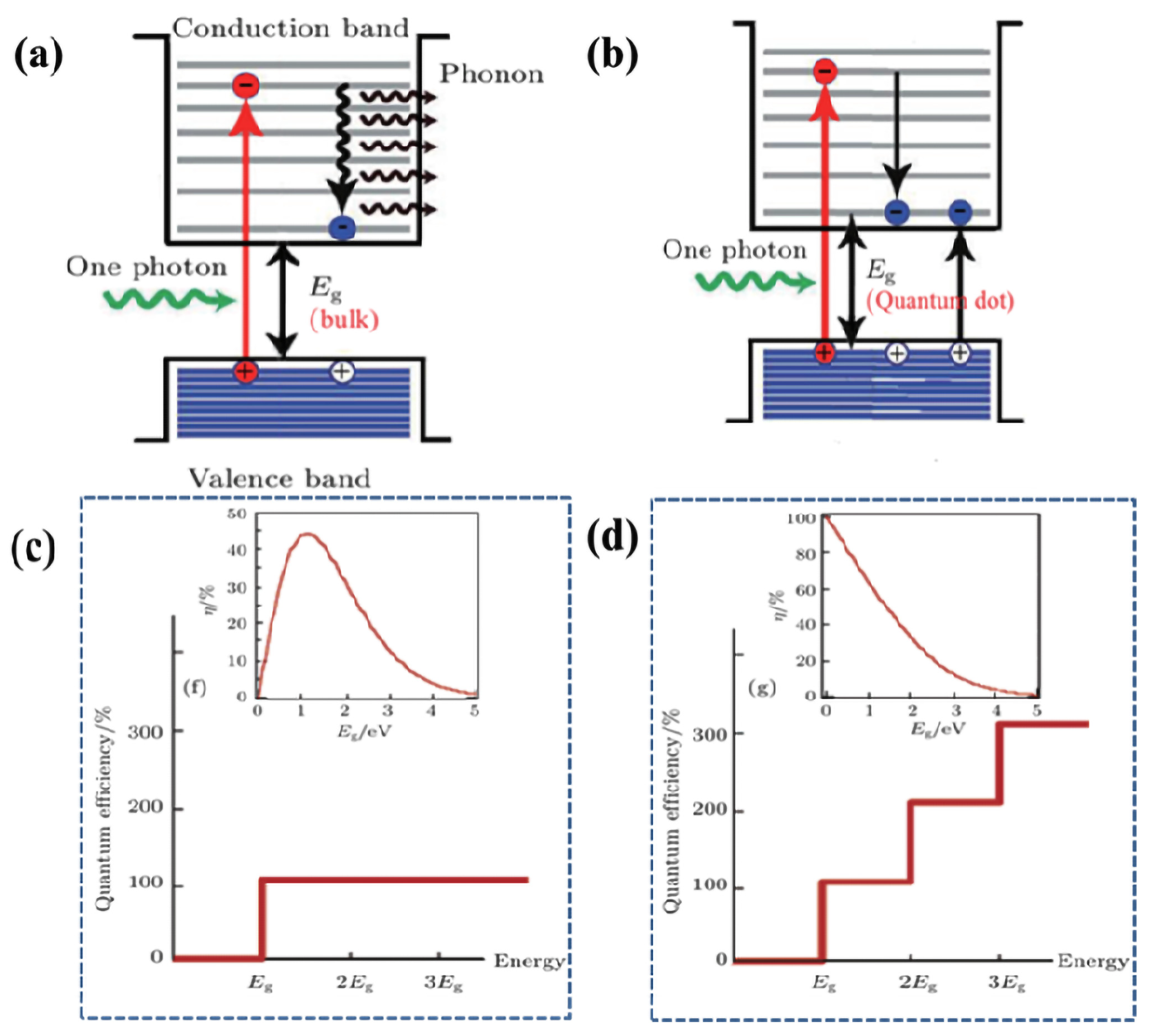
2.2. Multiple Exciton Generation

Multiple exciton effect (MEG) refers to the physical process by which two or more electron–hole pairs are generated after a high-energy photon is absorbed by nanomaterials. Nanomaterials are made from semiconductor materials such as silicon and gallium arsenide that have many excellent properties. For example, the quantum tunneling effect in nanoscale semiconductor materials leads to anomalous electron transport, reduced conductivity, and a decrease in electrical conductivity with a decrease in particle size, potentially leading to negative values. These characteristics play an important role in fields such as large-scale integrated circuit devices and optoelectronic devices. This effect usually occurs in quantum dot materials and thin film materials, which have not only important basic research significance but also potential application value in the field of new and high-performance optoelectronic devices. When a semiconductor material absorbs a photon, it generally produces a pair of hot carriers with certain kinetic energy. In the traditional photoexcitation process, a hot carrier collides with the lattice, and the radiating phonons relax to the band edge at a picosecond time scale (Figure 1a) [51]. Figure 1c shows that photon energy cannot be absorbed when the energy is lower than the band gap width, combination of electron–hole pairs, junction potential difference, and contact potential difference, as well as other loss factors. Nano-crystals have atom-like discrete energy levels, and their band gap Eg (the difference between the highest occupied and lowest unoccupied energy states) is regulated by their scales, which reduces the phonon radiation probability, leading to slower relaxation of electrons, effectively inhibiting Auger recombination [52,53,54,55]. On the other hand, the surface electrons of nanocrystals are increased, and the interaction between electrons is enhanced, thereby enhancing the coulomb interaction [53]. In addition, because the scale of the nanometer semiconductor is small, providing limited space for the area of the carrier, the momentum is no longer conserved [56]. Therefore, nanomaterials absorption occurs after high-energy photons produce a hot electron; as a result of auger recombination effectively restraining and enhancing the coulomb interaction, the hot electron is no longer in the form of phonon radiation cooling but stimulates the ground-state electronics and relaxes the bottom of the conduction band, as shown in Figure 1b [57]. In this process, when the photon energy is higher than the energy threshold Eth > 2Eg, the nanomaterials can produce two or more electron–hole pairs, whose multiple exciton generation efficiency is characterized by the EQE (i.e., absorbing a single photon and the number of electron–hole pairs generated within it) [58]. The traditional light absorption process of absorbing a single photon generally only produces one electron–hole pair, and the EQE is a straight line at Eth > Eg (Figure 1c). The ultimate efficiency of energy conversion reaches its maximum at Eg = 1.1 eV, which is 44%. Additionally, the number of electron–hole pairs produced by the multi-exciton effect process is related to the energy of incident photons. The efficiency of IQE after a change is shown in Figure 1d, and the ultimate efficiency of the energy conversion is close to 100% when Eg approaches zero [59].

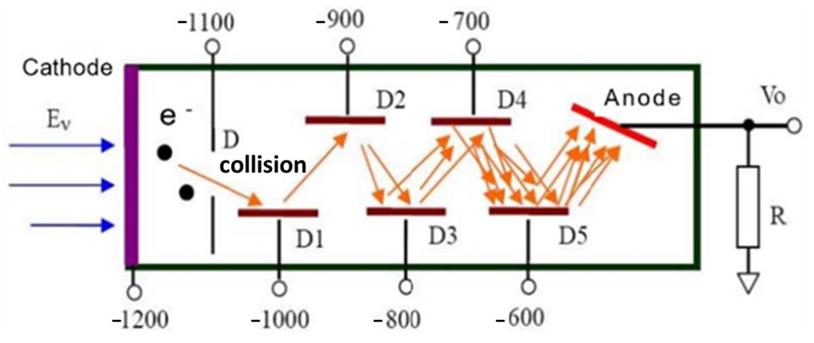
2.3. Semiconductor Avalanche Effect

In a high-voltage field, the semiconductor carrier will be electric heating (see the hot carrier in the semiconductor). Part of the carrier can obtain high enough energy, and the carrier may, through collision, transfer energy to electrons and lead to ionization, resulting in an electron–hole pair creation. This process is called impact ionization [60,61,62]. The carrier impact ionization rate is dependent on electric field intensity and represents a function of temperature (as the temperature increases, lattice scattering increases, which tends to hinder the heating of the carrier; usually, the ionization rate decreases with an increase in temperature), in which electrons and holes generally have different ionization rates [63,64]. The resulting electron–hole pairs, which move in opposite directions in the electric field, are heated by the electric field and generate new electron–hole pairs. In this way, a large number of carriers can be exponentially increased. The working mechanism is shown in Figure 2a. This phenomenon is called the avalanche multiplier effect and causes the breakdown of the P–N junction [65,66,67]. For a P–N junction with reverse bias, there is a strong electric field in the space charge area. When the reverse bias is high enough, and the electric field is strong enough in the space charge area, an avalanche multiplier effect will be generated as the thermal carrier passes through the strong electric field area (as shown in Figure 2c). The reverse current then increases rapidly with the reverse voltage through a phenomenon known as avalanche breakdown [68,69]. In 2019, a novel semiconductor avalanche mechanism was verified in a two-dimensional material InSe/BP vertical heterojunction device; the physical mechanism of a ballistic avalanche device is shown in Figure 2b [70]. Figure 2d shows the ballistic avalanche effect and quantum ballistic transport combined with the avalanche breakdown process. Here, the use of a ballistic transport charge presents almost no scattering and can maintain the quantum properties of the phase. Combining the nanoscale-controlled avalanche effect in the realization of carrier multiplier amplification while also maintaining low power consumption and low noise is expected to solve the working voltage of traditional devices encountering large avalanches, as device size currently represents a technology bottleneck.

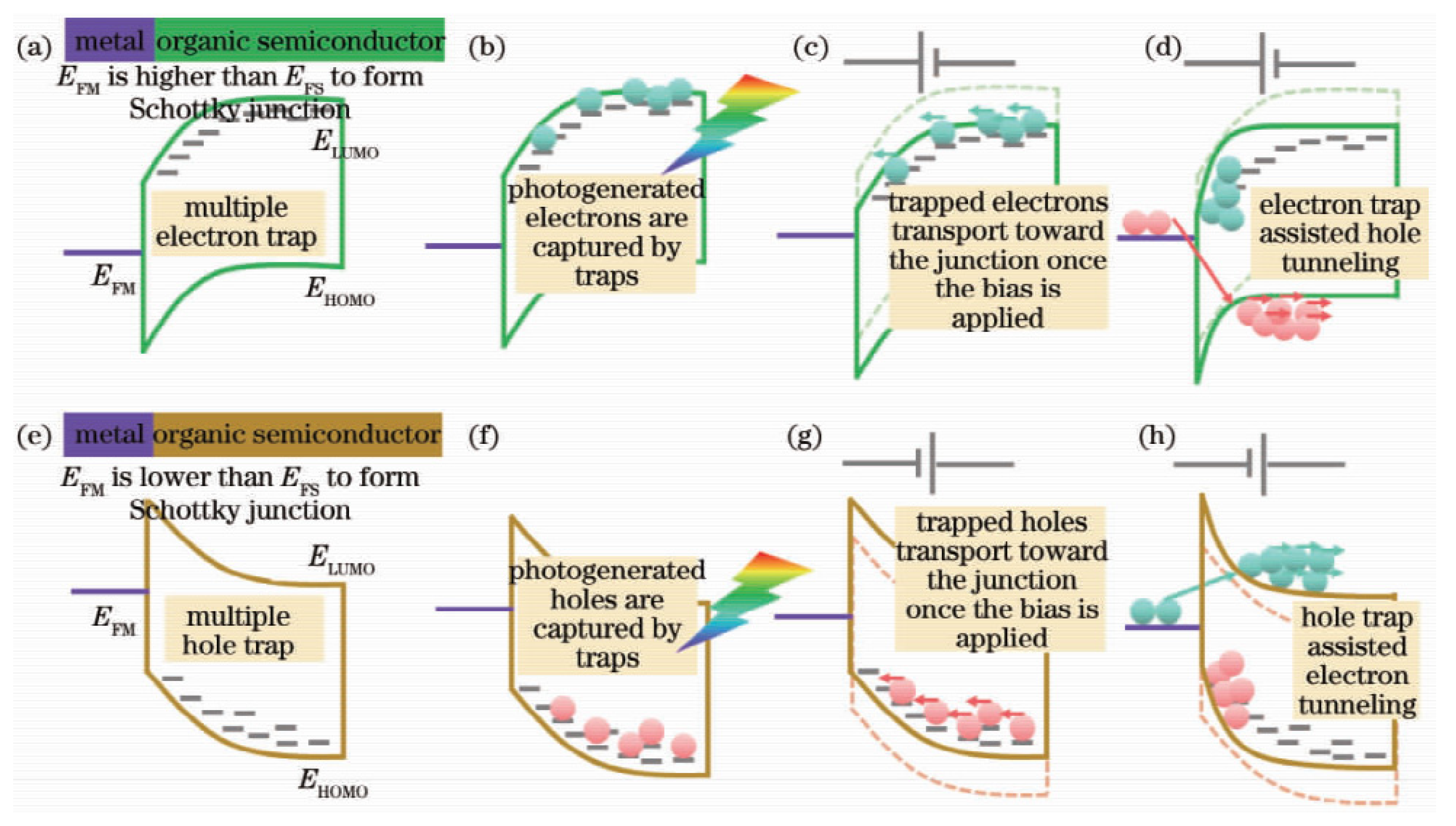
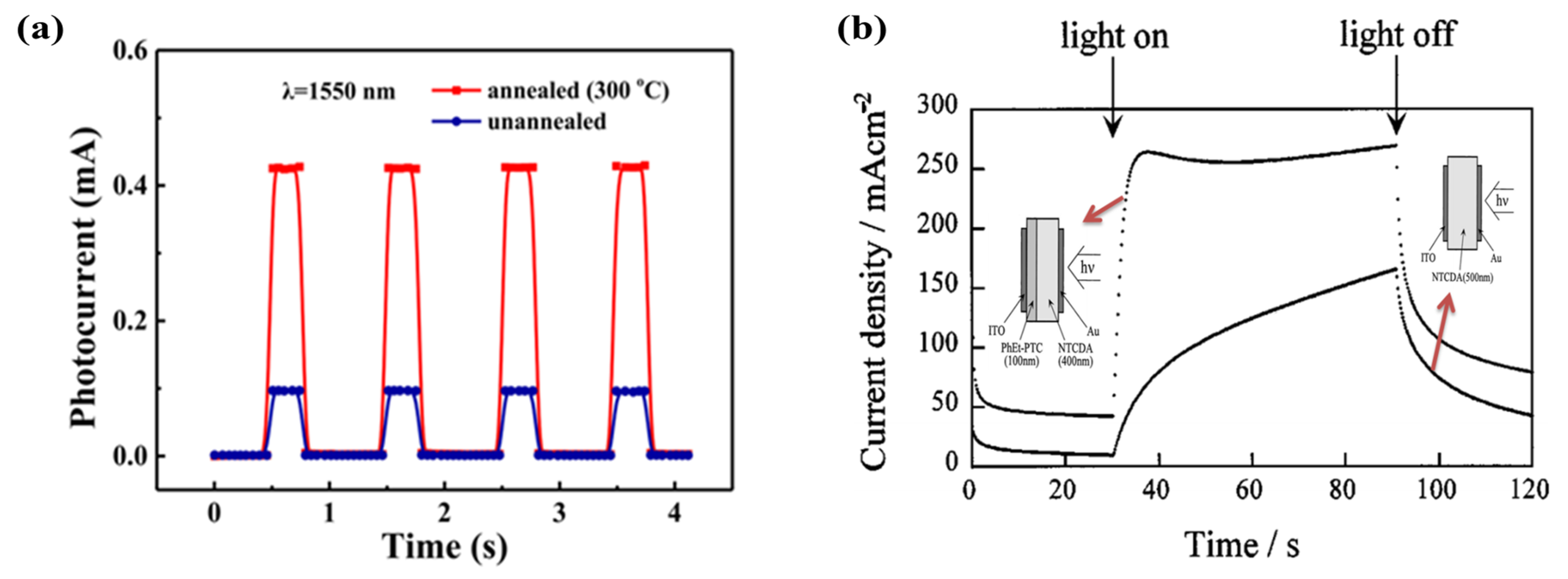
2.4. External Circuit Carrier Injection Organic Photomultiplier Effect

The working principle of the organic photomultiplier detector is to use the electron trap to help the hole form a tunneling effect or to use the hole trap to assist the electron in forming the tunneling effect, so as to produce a large number of carriers in the external circuit injection loop and finally achieve an external EQE far beyond 100%. When the metal electrode comes into contact with an organic semiconductor, the Fermi level (EF) of the metal electrode is different from that of the organic semiconductor material, resulting in a band bend at its interface, which is referred to as Schottky contact [71,72,73]. When the Fermi energy level of the metal electrode is higher than the EF of the organic matter, the semiconductor materials and electrons will flow from the metal-organic semiconductor and from the electrode to the organic semiconductor layer field formed by built-in electricity. As shown in Figure 3a, band bending, which forms a downward bend at the interface between organic materials, hinders the diffusion of organic semiconductors into the electrode. To achieve band bending (Figure 3a), low-power function electrodes such as Ag, Al, and Mg are usually required. When the Fermi level of the metal electrode is lower than that of the organic semiconductor materials, electrons will flow out of the organic semiconductor electrode. At this stage, the organic semiconductor layer formed refers to an electrode with an internal electric field. The corresponding band bending is shown in Figure 3e. This process forms an upward bend at the interface between organic materials, which prevents the diffusion of organic semiconductor electrons towards the electrode. The band bending shown in Figure 3e can be constructed using Au, indium tin oxide (ITO), Pt, and other high-power metals. In practice, the electrode surface can be modified to adjust the electrode work function and further adjust the band bending [74,75]. This effect can also be applied using conventional semiconductors.

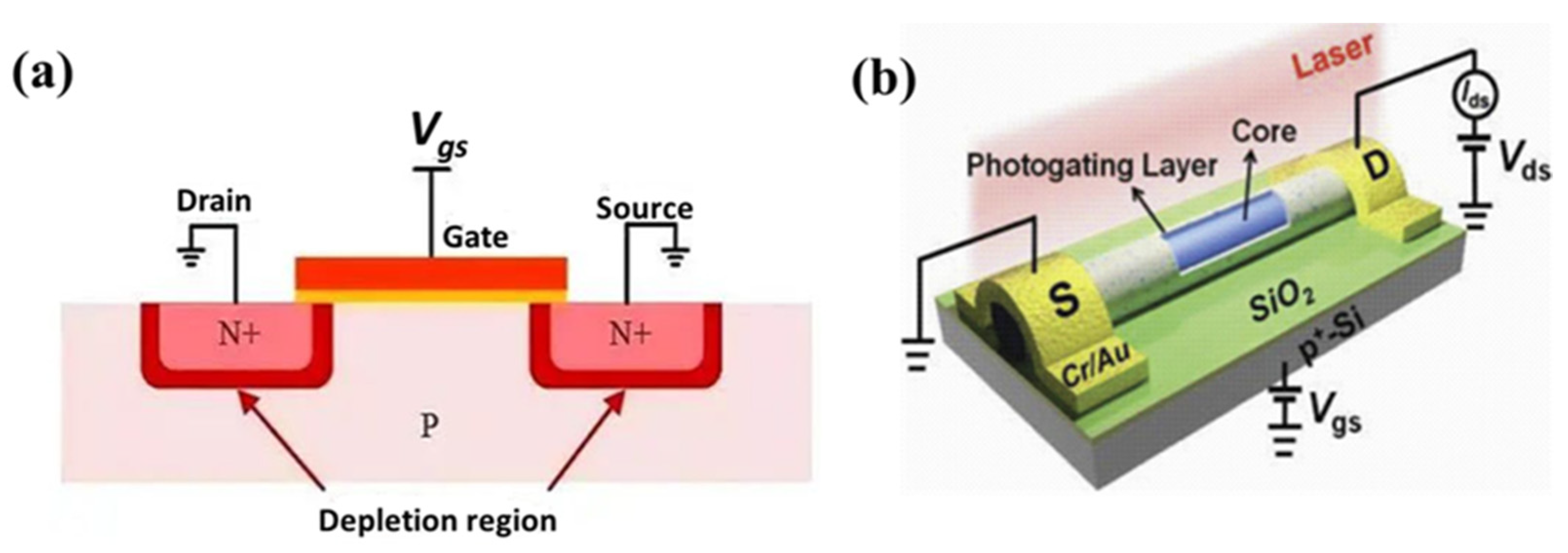
2.5. External Grid Control Mechanism

The electrostatic modulation capability of the transistor structure can be used to change the carrier concentration of the material in a controllable and reversible manner, thus altering the electrical and optical properties of the materials [76,77,78]. The traditional transistor structure includes the source drain, conducting channel, and gate used to regulate channel conductance. The typical channel is relatively thin. The source leakage at both ends of the channel provides extremely low resistance and has ohmic contact characteristics [79,80]. The gate electrode and channel form a capacitive structure for the metal insulator semiconductor. When voltage exists at both ends of the channel, interface charge is induced at the interface between the gate medium and semiconductor, and the electric field passing through the semiconductor also induces band bending at the interface of the gate medium semiconductor. Since the movement of the Fermi energy level with respect to the conduction band or valence band will change the moving charge and interface conductance at the channel interface, the carrier concentration at the channel interface will accumulate or be exhausted by an applied electric field in relation to the channel volume concentration. The structure of a typical type of FET is shown in Figure 4a. Depending on the gate voltage, this type of device will have one of three operating modes: depletion, accumulation, or inversion. The induced charge does not change the channel conductance until the gate voltage reaches the threshold voltage of the device. In addition, there is a new kind of regulation mechanism—photogating effect, which can be simply interpreted as light raw potential regulation and a control function, usually for the “core–shell” structure of nanowire transistors. Not only does the light-incident photon increase the number of free carrier “nuclear” layers, but also the “shell” layer surface state captures some photo-production carrier forming a type of “floating gate”, further regulating “nuclear” layer conductance and enabling nanowire transistors to be generated because less photon irradiation leads to a larger current and high gain. A typical structure is shown in Figure 4b [81,82,83].

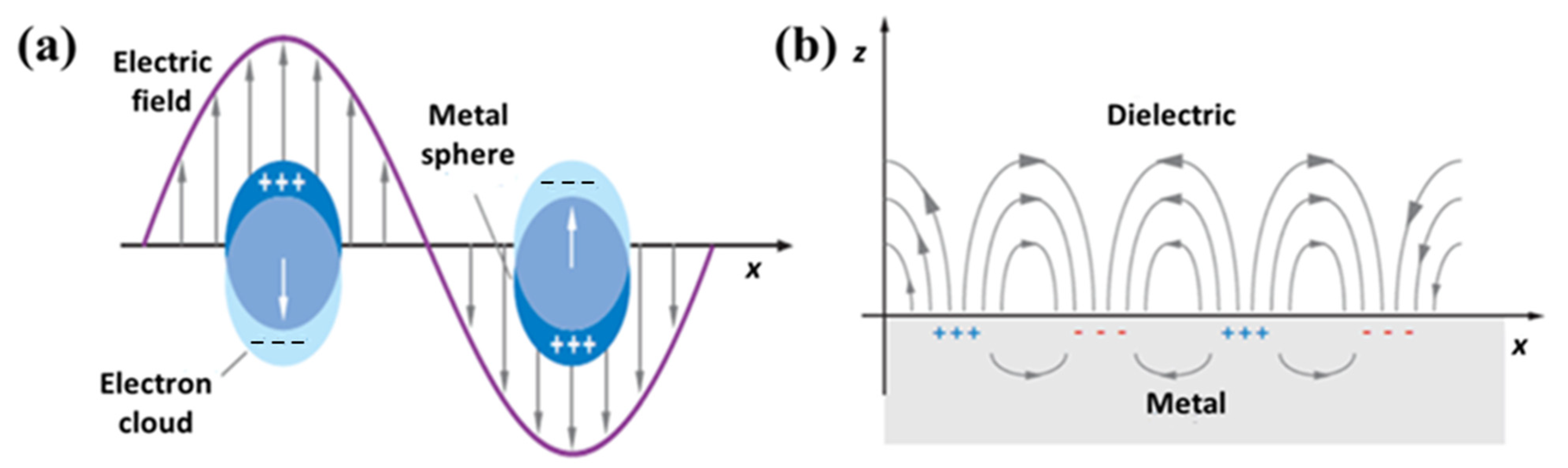
2.6. Regulation Effect of Micro–Nano Structure

Micro–nano optical enhancement mainly utilizes surface isoexciters, the near-field enhancement effects of the plasmon, the micro–nano optical junction, and the reflective optical junction to improve device performance. The medium local surface isopolarization and propagation surface isopolarization are the elementary excitation generated by the interaction between light and free electrons in the metal. At a subwavelength scale, these forms of excitation constrain the light field and transmission characteristics, thus breaking the diffraction limit, as shown in Figure 5 [84,85,86]. Like a laser, the characteristic size of a resonator can be as small as the submicron, deep submicron, or even nanometer level. The loss caused by joule heating is a bottleneck in the application of linear energy transfer (LET) components because of electron oscillation. In addition, by relying on local resonance such as electromagnetic field enhancement and slow light effect mechanisms, the micro–nano optical structure can effectively control light and matter (atomic, molecular, quantum dots, nonlinear material, etc.), the interaction of features, surface plasmon (using the plasmon near-field enhancement effect in the direction of the surface electric field parallel to the growth direction of the electronics), and photonic quantum-well-coupling resonance waves, as well as improve the absorbing ability of the quantum well to align the incident light, thereby improving the detection efficiency of infrared detectors [87,88,89,90].

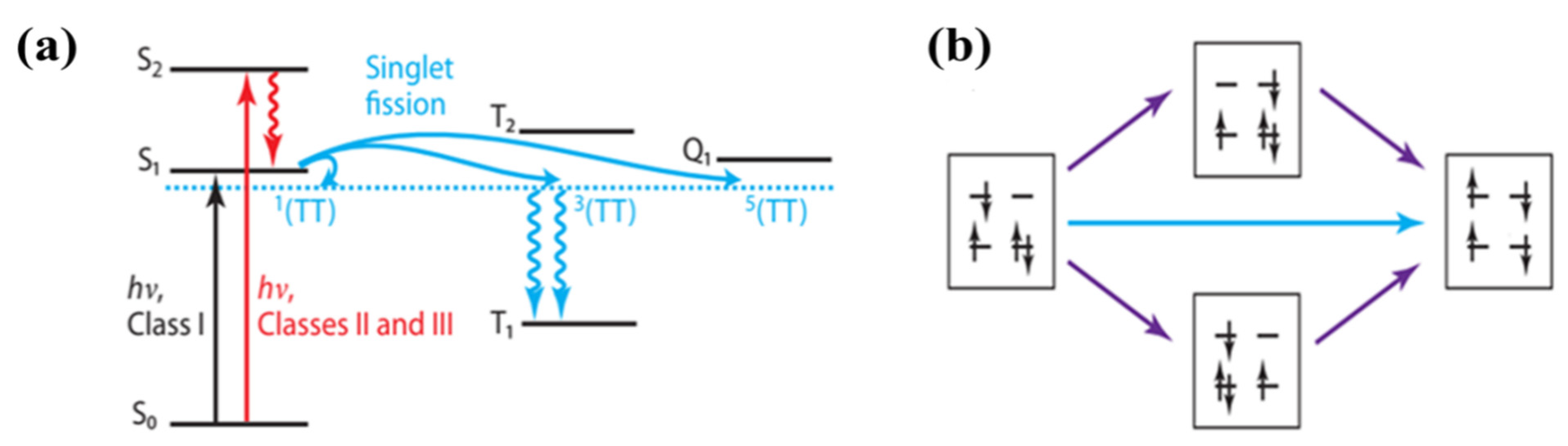
2.7. Singlet Fission Effect

Singlet fission (SF) is a process by which a singlet excited state (S1) is converted into two triplet excited states (T1) within a molecular system (Figure 6). The paper defining the term SF was published in 1963, in which Singh and Stoicheff used the context of SF to explain their observations in anthracene crystals [91]. In the following years, similar observations were reported for tetracene crystals [92,93,94]. This term was mainly used to explain the occurrence of delayed fluorescence, which was also used to identify and indirectly confirm this phenomenon [95,96,97,98,99,100]. Likewise, SF was later observed in carotenoids and conjugated polymers [101,102]. The conversion efficiency of photoelectric devices can be improved using the SF effect. Molecular dimers, especially those derived from pentacene, offer a versatile platform to understand many of the individual processes and spin states along the SF pathway, and several fundamental milestones have been reached.

3. Classification of Photomultiplier Detectors

According to different core-sensitive materials, photomultiplier detectors can be divided into inorganic photomultiplier detectors, organic photomultiplier detectors, and organic and inorganic photomultiplier detectors, which are based on a new 2D material photomultiplier detector. This section will summarize and analyze the performance and prospects for all types of photomultiplier detectors, introduce the performance, advantages, and disadvantages of all types of devices, and highlight the potential for further research and development, as well as future development directions.

3.1. Traditional Inorganic Photomultiplier Detector

Inorganic photomultiplier detectors mainly include photomultiplier tubes (PMTs), avalanche photodiodes (APDs), frequency up-conversion, and superconducting nano-wire single-photon detectors (SNSPDs).
PMTs are vacuum tubes used to detect very weak light. Since the first PMT was first made in 1936, they have been widely used commercially [103,104,105]. As shown in Figure 7, PMTs are composed of a photocathode, a double-level electron optical system, and an anode. The vacuum protection shell of the photocathode is formed by a functional, small, alkali metal compound coating. In the photocathode, when a certain energy of photon irradiation occurs outside the photoelectric effect, the photons become electrons, and electronic constraints through the electronic optical system in the electric field are doubled. The electronic grade is accelerated after bombardment, multiplied by the electric field on the surface of the secondary electron materials, thereby realizing the multiplication of electronic and electrical signals after the multi-stage multiplier reaches 105–109 times that of the amplifier. The amplifier output signal is the anode after collection [106,107]. In general, PMTs have a large detection area and extremely high sensitivity and gain. However, PMTs have the disadvantages of low time resolution, a large physical size, and a demanding working environment.
APDs have high internal gain and frequency response characteristics, which are usually formed through heavy doping at the P–N junction [108,109,110]. The APD usually works under high inverse bias pressure. When the incident photogenesis carrier in the absorption layer collides and dissociates, the carrier and lattice inside the device will produce an extremely strong avalanche multiplier effect, which can amplify the photocurrent generated by a single carrier to a macroscopic level that can be detected [111,112,113]. The basic structure of APD is the PN junction under reverse bias. When a photon enters into an electron in the absorbed region, an electron–hole pair will be generated. Under the action of the reverse bias electric field, the electron–hole pair will drift in different directions to form a photocurrent. Compared to PMTs, semiconductor APD devices are small in size, low in production cost, and do not require high vacuum working conditions. However, due to the band gap of semiconductor materials, the APD working waveband is concentrated in the visible to near-infrared regions.
The core of frequency up-conversion detection technology is to convert long-wave photons into short-wave photons that can be easily detected [114,115,116,117]. The principle is to generate frequency changes through the sum frequency effect of nonlinear optical crystals. Meanwhile, a weak light signal with frequency A and a strong pump light with frequency B are injected to generate the output light with frequency C under certain conditions. Under a sufficiently strong pump light, the conversion efficiency is very high while preserving the quantum properties of the input signal photons. For example, in periodically polarized lithium niobate crystal, the incident signal light of 1550 nm can be converted into light of 630 nm under the action of 1064 nm pump light, which can be detected by the existing silicon avalanche photonic avalanche photodiode, whose conversion efficiency can reach more than 90% [116]. At present, the main challenge of frequency conversion single photon detection technology in practical applications is that it requires strong pumping light. If the pump light is concentrated in a small area through the waveguide to improve the intensity, the waveguide input and output losses will be higher, as will the background noise.
Recently, an SNSD utilizing the critical temperature effect of superconductors to detect photomultiplication was developed. The initial superconducting nanowires operate at ultra-low temperatures below the superconducting threshold temperature (1.5~4 K), and the operating current is below the critical current. When one or more incident photons are absorbed by nanowires, the local thermal effect will be triggered, making the local temperature higher than the threshold temperature of superconductivity. The material near the absorption point will then change from a superconducting state to a resistance state, which will lead to the current passing around the point, thus making the surrounding current density exceed the critical current and transform into a positive normal state. This trend will continue to expand and form a resistance partition across the nanowire, causing the wire’s resistivity to rapidly increase and creating a detectable voltage pulse that enables avalanche photon detection. To improve the photosensitive surfaces of devices, nanowires are usually made into winding bands [117]. Due to the occurrence and recovery time of thermal effects, the time jitter of SNSPD is very low—only about 100 ps in large-array detectors and lower than 50 ps in small-array detectors [118]. Although SNSPDs are characterized by high speed, sensitivity, and no posterior pulse [119,120,121], they are currently limited by their material growth and preparation processes. To achieve superconductivity, SNSPDs need to operate below the temperature of liquid helium. However, with the emergence of the next generation of efficient devices, SNSPDs will be widely used in the field of quantum information [122].

3.2. Organic Photomultiplier Detectors

Organic photomultiplier detectors (OPMDs) can be divided into two types, small molecular- and polymer-based detectors, based on the different materials in their active layers. Because the synthesis method for organic materials is simple, the energy level structure can be designed freely. These materials also have the advantages of low cost, easy processing, environmental friendliness, and flexibility [74,123]. In recent years, photodetectors based on organic materials have been successively reported [123,124,125,126,127,128,129,130,131,132,133,134,135]. However, collision ionization cannot be realized in organic semiconductor materials because the binding energy of excitons in organic semiconductors is approximately 0.1~0.4 eV, which is about three orders of magnitude higher than that of inorganic semiconductor materials [126]. In 1994, Hiramoto et al. reported the first OPMD. Subsequently, a series of in-depth studies were carried out in this direction [127]. Organic photomultiplier detection technology has been developed for more than 20 years. The structure of this technology has transformed from simple to heterogeneous, and its performance has been constantly optimized. The working principle of OPMD is to use an electron trap auxiliary hole to form a tunneling effect or to use a hole trap auxiliary electron to form the tunneling effect, so as to produce a large number of carriers in the external circuit injection loop and achieve an EQE far beyond 100%.

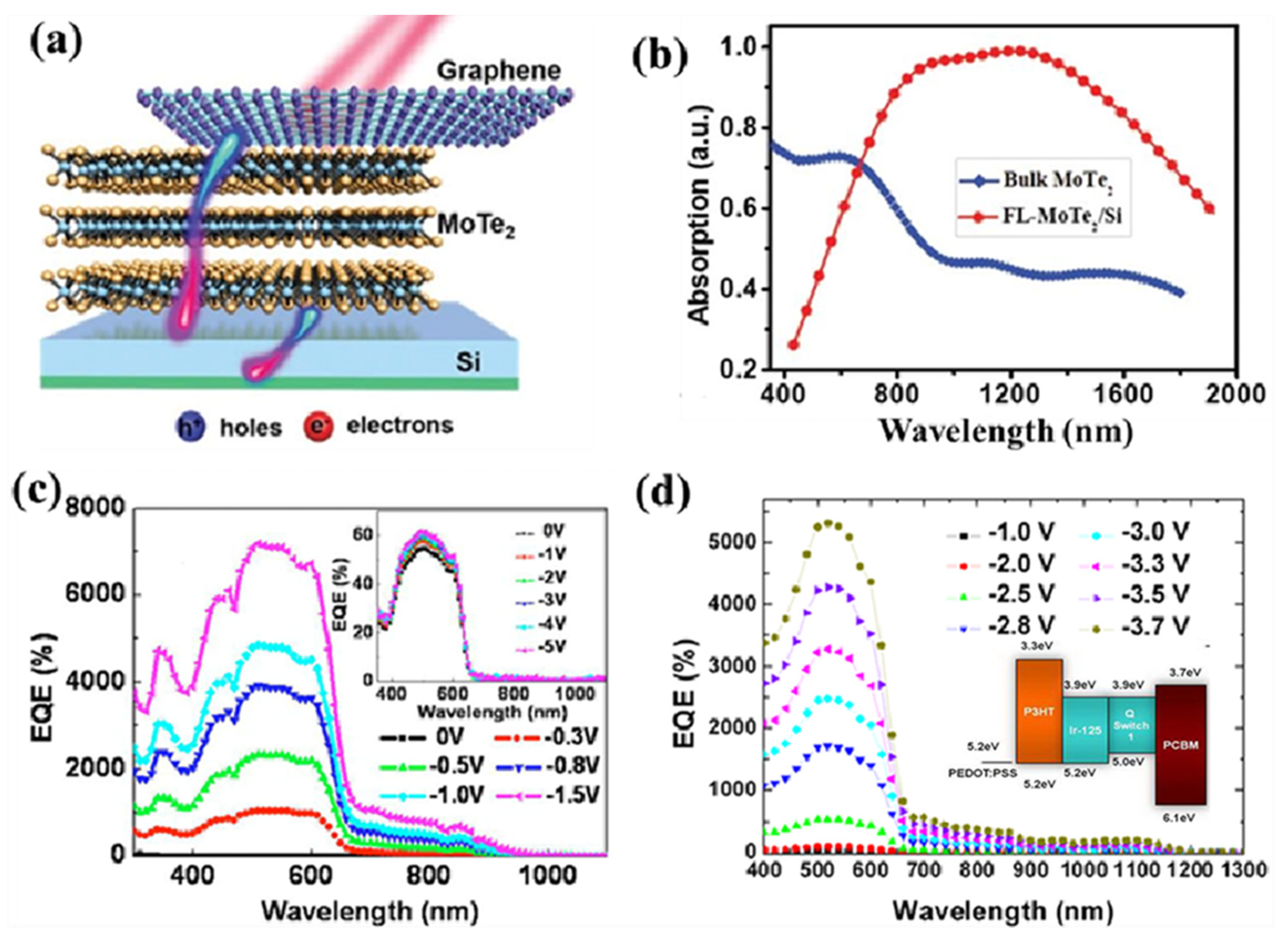
3.3. Two-Dimensional Material Photomultiplier Detectors (2D PMDs)

Two-dimensional materials represented by graphene have excellent semiconductor properties such as high carrier mobility and wide spectral response ranges, but their Ri values (~0.01 A/W) and optical gain effects (external EQE: 0.1%~0.2%) are extremely low due to the absence of a band gap and the presence of natural defects [128,129]. Zhang et al. obtained a pure graphene photodetector with high Ri (8.61 A/W) and high optical gain by re-designing the device structure [130]. Due to the limitations of the material itself, the photocurrent response characteristics of intrinsic 2D photodetectors cannot meet the demands of actual use, so a composite material structure system is required, as the different components of materials in such a system can compensate for each other in terms of performance. Additionally, a composite photodetector in the range of spectral response, Ri, and mobility, D*, could improve the detection rate of performance parameters. Compared to a single material, the optical response degree of the composite structure photodetector can generally be improved by more than 10 times, and some can even be improved by more than 1000 times [131,132,133]. The structure of such a photodetector is mainly divided into two types. In one type, when the current flows through the closed loop, it needs to pass through different types of materials (i.e., heterojunctions). In the other type, when the current flows through the closed loop and needs to pass through different types of materials, a channel conductive matrix is used to improve the material’s photoelectric properties through sensitization.

3.4. Organic/Inorganic Heterojunction Photomultiplier Detector

Inorganic materials have the advantages of high carrier mobility, high stability, and long service life, but their absorption band is narrow, there are fewer kinds of optional materials available, and they entail a high production cost. Additionally, organic materials are low cost, transparent, flexible, lightweight, and can be easily processed. However, they also have a low dielectric constant and low carrier mobility. These characteristics, through an effective combination of organic and inorganic materials, foster the material’s strengths and circumvent its weaknesses, enabling the preparation of more flexible components, such as photovoltaic devices, for the P–N junction [134,135]. There are currently two approaches toward developing organic/inorganic heterojunctions: One involves implementing a heterojunction with excellent properties [136,137,138,139,140]. The other involves improving the properties of inorganic materials by modifying organic molecules on inorganic materials. The multiplier effect of photoelectric properties can be realized through the above two methods. Yang et al. obtained an EQE higher than 100% and a significant photovoltaic effect by using a planar vertical heterojunction composed of organic matter and topological insulators [141,142,143]. Most international research in the field has focused on the feasibility of exploring and realizing device performance along with organic/inorganic heterojunction structure design and optimization. Notably, studies considering the photoelectric characteristics of the micro-physical mechanism remain few in number. The micro mechanism in this research could help further optimize the heterojunction structure to ultimately achieve the controllable preparation of heterojunction devices with excellent characteristics.

4. Performance Optimization of Photomultiplier Detector

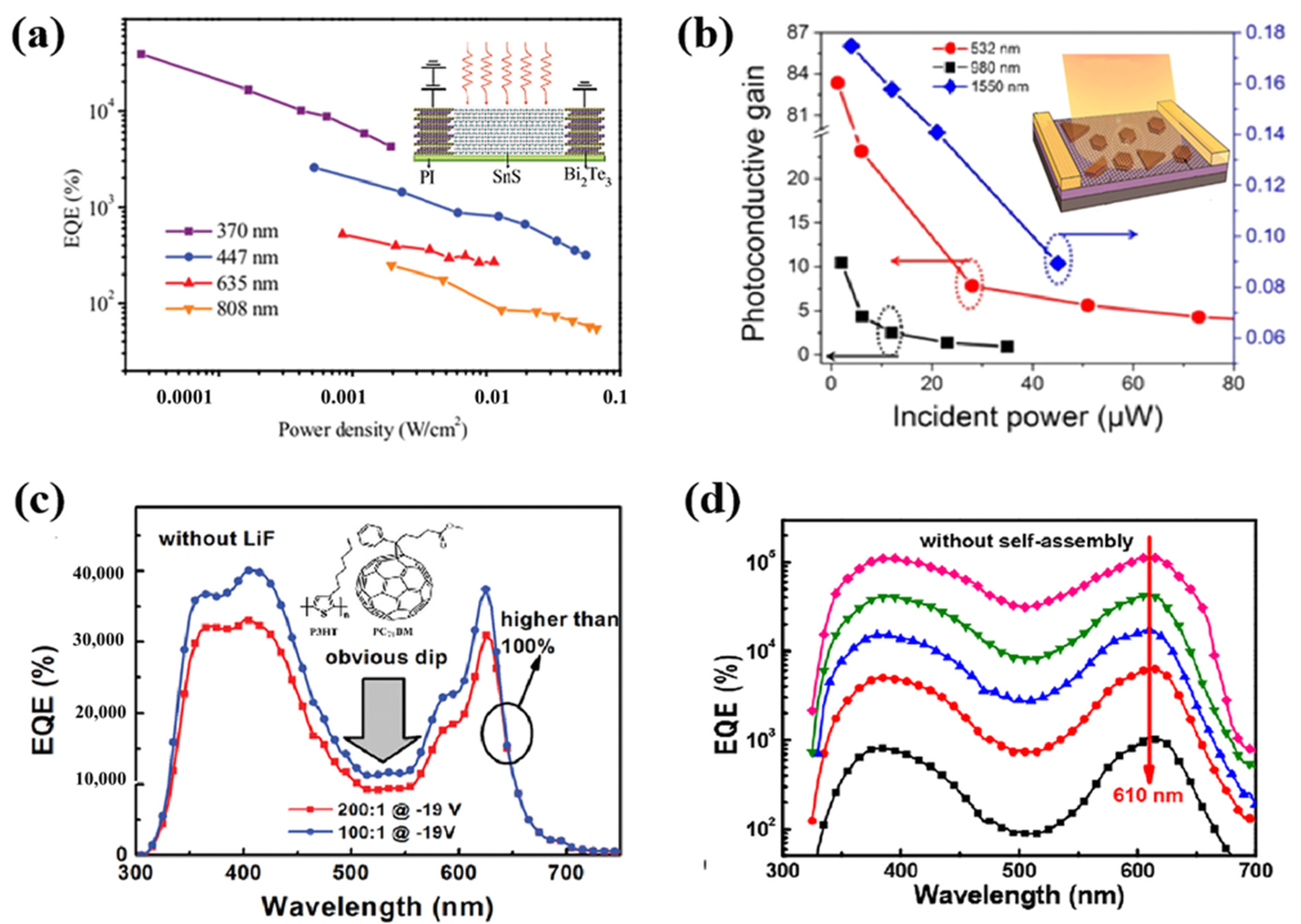
4.1. Improve the EQE of Devices

EQE is the key performance index for a photoelectric detector. Accordingly, the device detection rate will be most sensitive to this value. Under the same incident light intensity irradiation, a device with a higher EQE can output a higher photocurrent. Therefore, improving the EQE is an important aspect to optimize the performance of photodetectors. For inorganic materials, the EQE can be improved by using a structure of enhanced absorption. As shown in Figure 8a, Yao et al. designed a Bi2Te3/SnTe/Bi2Te3 photoelectric detector with an EQE of up to 1833% [144]. In addition, Figure 8b shows the use of a graphene/Bi2Te3 photomultiplier detector with optical enhancement architecture and an internal gain of 87 [145]. For small molecular-based organic photomultiplier detectors (Figure 8c), Nakayama et al. treated thin phET–PTC film with a tetrahydrofuran solvent, which significantly improved the photomultiplier performance of the device [146]. This study also showed that adjusting the evaporation rate of organic thin films can also change device performance and that a lower evaporation rate is conducive to obtaining devices with a higher photomultiplier coefficient (Figure 8d) [147]. For the bulk heterojunction polymer photomultiplier detector, through the insertion of different functional layers, the barrier width injected by the hole from the external circuit can be increased such that the EQE of the organic optoelectronic device can reach 37,500% [74]. Similar effects can also be achieved using organic materials to contact metal-like films, thereby achieving 100% EQE [141,142,143]. Currently reported devices with external EQE can exceed 105% [148]. To intuitively study the performance optimization of photomultiplier detectors, the performance of the relevant detectors mentioned above is outlined in Table 1.

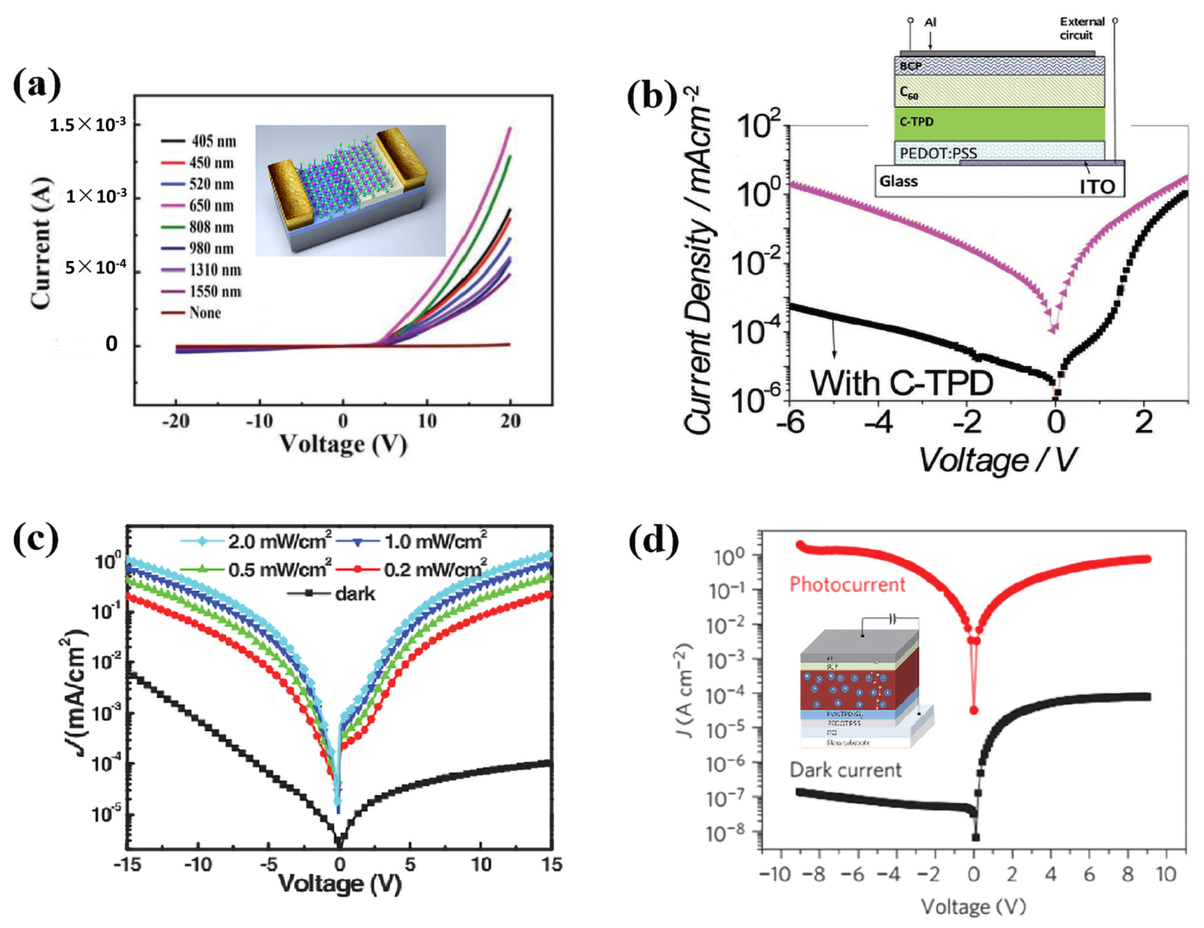
4.2. Reduce Dark Current

Reducing the dark current of the photodetector can help obtain a higher detection rate. When the response rates of different devices are equal, the lower the dark current of the device, the lower the equivalent power of its noise, and the weaker the optical signal able to be detected. The use of a heterojunction structure is one of the most effective ways to reduce the dark current of devices. Yang et al. prepared planar heterojunctions using molybdenum oxide and topological insulators (Figure 9a) and obtained a dark current lower than 1nA and a switch ratio of up to 105 [143]. Schottky contact can also reduce the dark current of the device, and electrode contact with 2D materials can reduce the dark current of the device by two levels [149]. In addition, organic devices can add different modification layers to reduce the dark current of the device (Figure 9b,c). For example, Huang et al. introduced a layer of C–TPD between PEDOT:PSS and C60 as the modification layer, which significantly improved the surface and internal morphology of the C60 thin film and reduced its dark current by three to four orders of magnitude [75,150]. Using an interface modification layer to block the injection of holes and carriers can also reduce the dark current of the device (Figure 9d) [151].

4.3. Adjust Response Speed

The response speed of photodetectors is also of concern to researchers. The photocurrent generated by a photomultiplier device is the carrier captured by the trap and drifting towards the junction area under the action of an electric field. This process requires significant time, and usually, the response speed of the device is slow. Thermal annealing is another good way to eliminate interface defects and enhance interface contact. As shown in Figure 10a, the response speed of heterogeneous junction devices can differ by two–three orders of magnitude depending on whether they are annealed or not [143]. Meantime, a series of studies were conducted to improve the response speed of small molecular-based organic photomultiplier detectors. For example, in 2000, Nakayama et al. compared the device properties of ITO/phET–PTC/NTCDA/Au and ITO/NTCDA/Au. The authors found that the film surface morphology obtained through evaporation and plating NTCDA on the ITO surface was very poor, but high-quality PHET–PTC film could be obtained on the ITO surface. This difference greatly improved the bias voltage that the device containing the PHET–PTC-modified layer could withstand [152]. Figure 10b shows the transient test performance of two different devices. It can be clear that the rising time of devices without a modification layer under a bias voltage of 12 V exceeded 60 s, while the rising time of devices with a modification layer under a bias voltage of 20 V was only 3.7 s. The introduction of this modification layer did not prevent multiplication behavior at the NTCDA/Au interface because the LUMO energy level of PHET–PTC was lower than that of NTCDA, enabling the electrons injected from the gold electrode to reach the ITO electrode successfully. In addition, the carrier transport performance of the active layer could be improved to improve the response speed of the device [153,154].

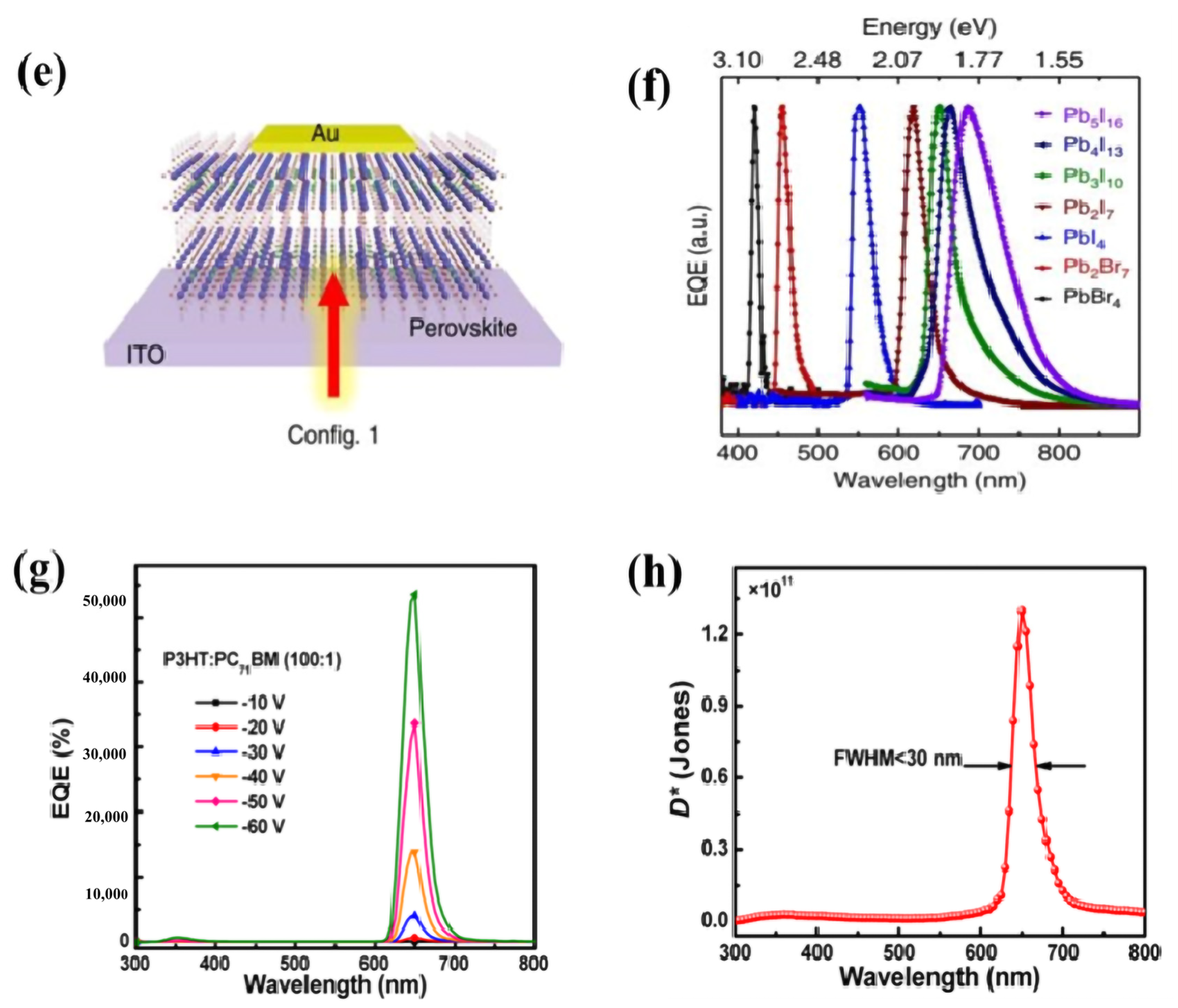
4.4. Adjust the Spectrum

The spectral adjustment of the detector mainly includes broadening and narrowing. The main way to broaden the band of the detector is to introduce new sensitive layer materials. For example, Lu et al. created a heterogeneous junction structure by adopting a few layers of MoTe2–Si composite (the device structure diagram is shown in Figure 11a). The photoelectric detector has a wide spectral response of 300–1800 nm (the absorption diagram is shown in Figure 11b), which widened the response range of the SI-based photoelectric detector in the near-infrared waveband [155]. The unique vertical N–N heterojunction design and the preparation of ultra-thin layered MoTe2 film provide a new direction for the construction of high-speed, wide-spectrum, silicon-compatible 2D–3D heterojunction photodetectors. At the same time, doped organic dyes can be used to broaden the response of the device in the infrared band. In 2010, Chen et al. not only achieved a breakthrough through the incorporation of IR-125 organic dye by avoiding the appearance of a photomultiplier effect in the P3HT/PCBM heterojunction device with a mass ratio of 1:1 but also greatly broadened the response spectrum of the device, as shown in Figure 11c [156]. Compared to devices without dye doping, devices doped with IR-125 showed a significant photomultiplier effect in the near-infrared band, with EQE values exceeding 100% in a wavelength range of less than 900 nm. Subsequently, the dye IR-125 and Q-Switch were combined into a P3HT/PCBM active layer to further improve the response of the device in the infrared band, as shown in Figure 9d [157]. A series of material doping results followed, all with fairly good results [158,159].
Low-cost narrow-band detectors are urgently needed in the fields of national defense, fluorescence microscopy, and surveillance technology. An ideal narrow-band response of the detector offers good shielding against external light, high EQE values at a specific wavelength, low noise current (dark current), and, most importantly, an ideal half-peak full-width at half maximum [160,161,162]. There are two methods commonly used to obtain an ideal narrow-band response from a photomultiplier detector. First, color filters are used to select the response to a specific wavelength, but this can lead to optical attenuation, which reduces the optical response rate of the device. Moreover, the introduction of additional color filters can make the system relatively complex. Narrow-band UV response photodetectors can be prepared using wideband gap materials. Li et al. used two-dimensional perovskite materials to create a narrow-band photodetector with a highly tunable external EQE (200%), ultra-low dark current (10−12 A), and a high switching ratio (103). In addition, the spectral response of the narrow-band photodetector can be continuously modulated from red to blue light, and the full width at half-maximum (FWHM) of all detectors is less than 60 nm, especially in the blue light wavelength range, where the FWHM is less than 20 nm. This excellent performance can be attributed to the absorption of the self-trapping state below the band gap in the two-dimensional perovskite and the combined effect of extremely low conductivity in the outer direction of the crystal [163]. In addition, by thickening the active layer (2.5 m) and adjusting the carrier collection efficiency, Wang et al. achieved a narrow-band organic photomultiplier detector, as shown in Figure 11g,h. The highest EQE value was 5350%, and the full width at half-maximum of the detection rate spectrum was less than 30 nm [164].
Figure 11. Ph Photodetector that detects broadening and narrowing of the spectrum: (a,b) FL–MoTe2–Si-composite-made structure diagram of the heterogeneous device and a wide spectral absorption diagram of the photodetector at 300–1800 nm [155]. (c) Comparison of EQE curves of P3HT/PCBM doped with and without IR-125 organic dyes [156]. (d) P3HT/PCBM device’s co-active layer doped with IR-125 and Q-Switch1 dye material in the EQE curve [163]. (e,f) Schematic diagram of a two-dimensional perovskite narrow-band photoelectric detector structure and tunable photoelectric performance curve. (g,h) EQE curve and responsiveness curve of the P3HT/PC71BM (100:1) thickened active layer (2.5 m) [164].
Coatings 13 01088 g011aCoatings 13 01088 g011b

5. Conclusions and Challenges

Photodetectors are widely used in the military, the national economy, general life, and other fields. Specifically, photomultiplier detectors have attracted significant attention because of their extremely high EQE and G. Indeed, photomultiplier detectors based on inorganic, organic, and inorganic/organic combinations can be found in several everyday applications. These components could replace or update the optical switches in some existing electronic products, reducing the cost and product quality. Moreover, due to their adjustable response speeds, photomultiplier detectors could play an important role in industrial automatic control, distributed environmental monitoring, and other fields. In addition, new photomultiplier detectors, such as ballistic avalanche photodetectors, could be extended to the application fields of photodetectors, such as quantum communication, high-precision single-photon detection, and other new fields.
In this paper, we reviewed the effects of EQE exceeding 100%, including multiple exciton effects, semiconductor avalanche effects, carrier injection organic photomultiplier effects in external circuits, gate regulating micro–nano optical enhancement effects, material exciton fission effects, etc. The working principles and application prospects of these effects were also reviewed. We also sorted and classified the working mechanisms of new and traditional photomultiplier effects, APDs, and new ballistic avalanche effects on the organic photomultiplier, followed by exploring a new organic/inorganic device. Photomultiplier devices have great potential but also face many challenges, such as the following:
  • Analysis of gain mechanisms remains incomplete, and many sources of high-EQE device efficiency are still unclear.
  • There are still many problems in determining whether newly discovered effects can be applied to the fabrication of actual devices, which will require further research to resolve.
  • The response speed of reported photomultiplier detectors was found to be mostly in the order of milliseconds, which cannot meet the needs of high-speed photodetectors. How we can further improve the response speed of photomultiplier devices also needs to be further studied.
  • The stability of the device was not discussed in most existing work, and solving the stability problem is a key factor that must be overcome in the application of the device.
  • The introduction of a metal micro–nano structure has achieved great success in the field of solar cells. However, whether introducing a metal micro–nano structure into the photomultiplier detector would significantly improve device performance remains to be determined in future studies.

Author Contributions

M.Y. and J.C., conducted and designed the work. H.C. and X.Z., conducted experimental measurement. All authors discussed the experimental results and provided suggestions and assistance. All authors have read and agreed to the published version of the manuscript.

Funding

The authors thank the independent research project of fund project for basic scientific research expenses of Central Universities (ZJ2023-012, PHD2023-007), Sichuan Province Engineering Technology Research Center of General Aircraft Maintenance (No. GAMRC2021ZD01).

Institutional Review Board Statement

Not applicable.

Informed Consent Statement

Not applicable.

Data Availability Statement

Not applicable.

Acknowledgments

This review is dedicated to Ming Yang’s son Yixuan Yang, who was born on 1 June 2023.

Conflicts of Interest

The authors declared that they have no conflict of interest to this work. We declare that we do not have any commercial or associative interest that represents a conflict of interest in connection with the work submitted.

References

  1. Behura, S.; Wang, C.; Wen, Y.; Berry, V. Graphene-semiconductor heterojunction sheds light on emerging photovoltaics. Nat. Photonics 2019, 13, 312–318. [Google Scholar] [CrossRef]
  2. Pospischil, A.; Humer, M.; Furch, M.; Bchmann, D.; Guider, R.; Fromherz, T.; Mueller, T. CMOS-compatible graphene photodetector covering all optical communication bands. Nat. Photonics 2013, 7, 892–896. [Google Scholar] [CrossRef]
  3. Huang, Z.; Ji, C.; Cheng, L.; Han, J.; Yang, M.; Wei, X.; Jiang, Y.; Wang, J. Zero-bias visible to near-infrared horizontal p-n-p TiO2 nanotubes doped monolayer graphene photodetector. Molecules 2019, 24, 1870. [Google Scholar] [CrossRef] [PubMed] [Green Version]
  4. Liu, Q.; Yang, M.; Zhang, J.; Yang, M.; Wang, J.; Zheng, H.; Gou, J. Three-dimensional Dirac semimetal/organic thin film heterojunction photodetector with fast response and high detectivity. Front. Phys. 2021, 9, 672591. [Google Scholar] [CrossRef]
  5. Kang, K.; Li, T.; Sohn, E.; Shan, J.; Mak, K. Nonlinear anomalous hall effect in few-layer WTe2. Nat. Photonics 2019, 18, 324–328. [Google Scholar] [CrossRef] [PubMed]
  6. Peng, M.; Liu, Y.; Yu, A.; Zhang, Y.; Liu, C.; Liu, J.; Wu, W.; Zhang, K.; Shi, X.; Kou, J.; et al. Flexible self-powered GaN ultraviolet photoswitch with Piezo-phototronic effect enhanced on/off ratio. ACS Nano 2016, 10, 1572–1579. [Google Scholar] [CrossRef]
  7. Hu, X.; Zhang, X.; Liang, L.; Bao, J.; Li, S.; Yang, W.; Xie, Y. High-performance flexible broadband photodetector based on organolead halide perovskite. Adv. Funct. Mater. 2015, 24, 7373–7380. [Google Scholar] [CrossRef]
  8. Xu, L.; Wu, H.; Yao, G.; Chen, L.; Yang, X.; Chen, B.; Huang, X.; Zhong, W.; Chen, X.; Yin, Z.; et al. Giant voltage enhancement via triboelectric charge supplement channel for self-powered electroadhesion. ACS Nano 2018, 12, 10262–10271. [Google Scholar] [CrossRef]
  9. Pei, Z.; Zhu, M.; Huang, Y.; Huang, Y.; Xue, Q.; Geng, H.; Zhi, C. Dramatically improved energy conversion and storage efficiencies by simultaneously enhancing charge transfer and creating active sites in MnOx/TiO2 nanotube composite electrodes. Nano Energy 2016, 20, 254–263. [Google Scholar] [CrossRef]
  10. Han, J.; Wang, J.; Yang, M.; Kong, X.; Chen, X.; Huang, Z.; Guo, H.; Gou, J.; Tao, S.; Liu, Z.; et al. Graphene/organic semiconductor heterojunction phototransistors with broadband and bi-directional photoresponse. Adv. Mater. 2018, 2018, 1804020. [Google Scholar] [CrossRef]
  11. Zhao, B.; Wang, F.; Chen, H.; Zheng, L.; Su, L.; Zhao, D.; Fang, X. An ultrahigh responsivity (9.7 mA W−1) self-powered solar-Blind photodetector based on individual ZnO-Ga2O3 heterostructures. Adv. Funct. Mater. 2017, 27, 1700264. [Google Scholar] [CrossRef]
  12. Long, M.; Liu, E.; Wang, P.; Gao, A.; Xia, H.; Luo, W.; Wang, B.; Zeng, J.; Fu, Y.; Xu, K. Broadband photovoltaic detectors based on an atomically thin heterostructure. Nano Lett. 2016, 16, 2254–2259. [Google Scholar] [CrossRef] [PubMed] [Green Version]
  13. Ho, P.H.; Liou, Y.T.; Chuang, C.H.; Lin, S.W.; Tseng, C.Y.; Wang, D.Y.; Chen, C.C.; Hung, W.Y.; Wen, C.Y.; Chen, C.W. Self-crack-filled graphene films by Metallic nanoparticles for high-performance graphene heterojunction solar cells. Adv. Mater. 2015, 27, 1724–1729. [Google Scholar] [CrossRef] [PubMed]
  14. Ni, Z.; Ma, L.; Du, S.; Xu, Y.; Yuan, M.; Fang, H.; Wang, Z.; Xu, M.; Li, D.; Yang, J. Plasmonic silicon quantum dots enabled high-sensitivity ultra-broadband photodetection of graphene-based hybrid phototransistors. ACS Nano 2017, 11, 9854–9862. [Google Scholar] [CrossRef] [PubMed]
  15. Gan, X.; Shiue, R.; Gao, Y.; Meric, I.; Heinz, T.; Shepard, K.; Hone, J.; Assefa, S.; Englund, D. Chip-integrated ultrafast graphene photodetector with high responsivity. Nat. Photonics 2013, 7, 883–887. [Google Scholar] [CrossRef]
  16. McIver, J.; Hsieh, D.; Steinberg, H.; Jarillo-Herrero, P.; Gedik, N. Control over topological insulator Iphs with Light Polarization. Nat. Nanotechnol. 2011, 7, 96–100. [Google Scholar] [CrossRef]
  17. Lian, Y.; Han, J.; Yang, M.; Peng, S.; Zhang, C.; Han, C.; Zhang, X.; Liu, X.; Zhou, H.; Wang, Y.; et al. Tunable bi-directional photoresponse in hybrid PtSe2−x thin films based on precisely controllable selenization engineering. Adv. Funct. Mater. 2022, 2022, 202205709. [Google Scholar]
  18. Youngblood, N.; Chen, C.; Koester, S.; Li, M. Waveguide-integrated black phosphorus photodetector with high responsivity and low dark current. Nat. Photonics 2015, 9, 247–252. [Google Scholar] [CrossRef] [Green Version]
  19. Yang, T.; Wang, X.; Zheng, B.; Qi, Z.; Ma, C.; Fu, Y.; Fu, Y.; Hautzinger, M.P.; Jiang, Y.; Li, Z.; et al. Ultrahigh-performance optoelectronics demonstrated in ultrathin perovskite-based vertical semiconductor heterostructures. ACS Nano 2019, 13, 7996–8003. [Google Scholar] [CrossRef]
  20. Long, M.; Wang, Y.; Wang, P.; Zhou, X.; Xia, H.; Luo, C.; Huang, S.; Zhang, G.; Yan, H.; Fan, Z.; et al. Palladium Diselenide Long-Wavelength Infrared Photodetector with High Sensitivity and Stability. ACS Nano 2019, 13, 2511–2519. [Google Scholar] [CrossRef] [Green Version]
  21. Yang, M.; Wang, J.; Han, J.; Ling, J.; Ji, C.; Kong, X.; Liu, X.; Huang, Z.; Gou, J.; Liu, Z. Enhanced performance of broadband room temperature photodetector based on Cd3As2 thin film/pentacene heterojunction. ACS Photonics 2018, 5, 3438–3445. [Google Scholar] [CrossRef]
  22. Khanikaev, A.; Shvets, G. Two-dimensional topological photonics. Nat. Photonics 2017, 11, 763–773. [Google Scholar] [CrossRef]
  23. He, L.; Xiu, F.; Yu, X.; Teague, M.; Jiang, W.; Fan, Y.; Kou, X.; Lang, M.; Wang, Y.; Huang, G.; et al. Surface-dominated conduction in a 6 nm thick Bi2Se3 thin film. Nano Lett. 2012, 12, 1486–1490. [Google Scholar] [CrossRef] [PubMed]
  24. Zhang, E.; Wang, P.; Li, Z.; Wang, H.; Song, C.; Huang, C.; Chen, Z.; Yang, L.; Zhang, K.; Lu, S.; et al. Tunable ambipolar polarization-sensitive photodetectors based on high-anisotropy ReSe2 nanosheets. ACS Nano 2016, 10, 8067–8077. [Google Scholar] [CrossRef] [PubMed]
  25. Wang, C.; He, Q.; Halim, U.; Liu, Y.; Zhu, E.; Lin, Z.; Xiao, H.; Duan, X.; Feng, Z.; Cheng, R.; et al. Monolayer atomic crystal molecular superlattices. Nature 2018, 555, 231–236. [Google Scholar] [CrossRef]
  26. Zhang, R.; Zhang, S.; An, T.; Lu, G.; Yang, T. Photomultiplication type inverted organic photodetector based on PbS quantum dots. Opt. Mater. 2023, 138, 113722. [Google Scholar] [CrossRef]
  27. Windischhofer, P.; Riegler, W. Passive quenching, signal shapes, and space charge effects in SPADs and SiPMs. Nucl. Inst. Methods Phys. Res. A 2023, 1045, 167627. [Google Scholar] [CrossRef]
  28. Zhang, C.; Zhang, Y.; Yuan, X.; Lu, S.; Zhang, J.; Narayan, A.; Liu, Y.; Zhang, H.; Ni, Z.; Liu, R.; et al. Quantum Hall effect based on Weyl Orbits in Cd3As2. Nature 2019, 565, 331–336. [Google Scholar] [CrossRef]
  29. Maebe, J.; Vandenberghe, S. Effect of detector geometry and surface finish on Cerenkov based time estimation in monolithic BGO detectors. Phys. Med. Biol. 2023, 68, 025009. [Google Scholar] [CrossRef]
  30. Scott, R.; Jiang, W.; Jamal Deen, M. CMOS time-to-digital converters for biomedical imaging applications. IEEE Rev. Biol. Eng. 2023, 16, 627–651. [Google Scholar] [CrossRef]
  31. Sangwan, V.K.; Hersam, M.C. Electronic transport in twodimensional materials. Annu. Rev. Phys. Chem. 2018, 69, 299–325. [Google Scholar] [CrossRef] [Green Version]
  32. Konstantatos, G.; Sargent, E.H. Nanostructured materials for photon detection. Nat. Nanotechnol. 2010, 5, 391–400. [Google Scholar] [CrossRef]
  33. Sun, Z.H.; Chang, H.X. Graphene and graphene-like two-dimensional materials in photodetection: Mechanisms and methodology. ACS Nano 2014, 8, 4133–4156. [Google Scholar] [CrossRef]
  34. Beck, M.E.; Hersam, M.C. Emerging opportunities for electrostatic control in atomically thin devices. ACS Nano 2020, 14, 6498–6518. [Google Scholar] [CrossRef] [PubMed]
  35. Salvatori, S.; Pace, E.; Rossi, M.C.; Galluzzi, F. Photoelectrical characteristics of diamond UV detectors: Dependence on device design and film quality. Diamond Related Mater. 1997, 6, 361–366. [Google Scholar] [CrossRef]
  36. Robert, D. McKeag; Richard B Jackman. Diamond UV photodetectors: Sensitivity and speed for visible blind applications. Diamond Related Mater. 1998, 7, 513–518. [Google Scholar]
  37. Zhou, A.; Velázquez, R.; Wang, X.; Feng, P. Nanoplasmonic 1D diamond UV photodetectors with high performance. ACS Appl. Mater. Interfaces 2019, 11, 38068–38074. [Google Scholar] [CrossRef]
  38. Borelli, C.; Bosio, A.; Parisini, A.; Pavesi, M.; Vantaggio, S.; Fornari, R. Electronic properties and photo-gain of UV-C photodetectors based on high-resistivity orthorhombic κ-Ga2O3 epilayers. Mater. Sci. Eng. B 2022, 286, 116056. [Google Scholar] [CrossRef]
  39. Girolami, M.; Bosi, M.; Serpente, V.; Mastellone, M.; Seravalli, L.; Pettinato, S.; Salvatori, S.; Trucchi, D.M.; Fornari, R. Orthorhombic undoped j-Ga2O3 epitaxial thin films for sensitive, fast, and stable direct X-ray detectors. J. Mater. Chem. C 2023, 11, 3759. [Google Scholar] [CrossRef]
  40. Mazzolini, P.; Fogarassy, Z.; Parisini, A.; Mezzadri, F.; Diercks, D.; Bosi, M.; Seravalli, L.; Sacchi, A.; Spaggiari, G.; Bersani, D.; et al. Silane-mediated expansion of domains in Si-doped κ-Ga2O3 epitaxy and its impact on the in-plane electronic conduction. Adv. Funct. Mater. 2023, 33, 2207821. [Google Scholar] [CrossRef]
  41. Yang, M.; Wang, J.; Zhao, Y.; He, L.; Ji, C.; Liu, X.; Zhou, H.; Wu, Z.; Wang, X. Three-dimensional topological insulator Bi2Te3/organic thin film heterojunction photodetector with fast and wideband response from 450 to 3500 nanometers. ACS Nano 2019, 13, 755–763. [Google Scholar] [CrossRef]
  42. Yang, M.; Wang, J.; Yang, Y.; Zhang, Q.; Ji, C.; Wu, G.; Su, Y.; Gou, J.; Wu, Z.; Yuan, K.; et al. Ultraviolet to long-wave infrared photodetectors based on a three-dimensional Dirac semimetal/organic thin film heterojunction. J. Phys. Chem. Lett. 2019, 10, 3914–3921. [Google Scholar] [CrossRef]
  43. Jain, S.K.; Aggarwal, N.; Krishna, S.; Kumar, R.; Husale, S.; Gupta, V.; Gupta, G. GaN-UV photodetector integrated with asymmetric metal semiconductor metal structure for enhanced responsivity. J. Mater. Sci.-Mater. Electron. 2018, 29, 8958–8963. [Google Scholar] [CrossRef]
  44. Buscema, M.; Island, J.O.; Groenendijk, D.J.; Blanter, S.I.; Steele, G.A.; Van der Zant, H.S.; Castellanos-Gomez, A. Iph generation with two-dimensional Van der Waals semiconductors. Chem. Soc. Rev. 2015, 44, 3691–3718. [Google Scholar] [CrossRef] [PubMed] [Green Version]
  45. Xu, X.; Gabor, N.M.; Alden, J.S.; Van der Zande, A.M.; McEuen, P.L. Photo-thermoelectric at a graphene interface junction. Nano Lett. 2010, 10, 562–566. [Google Scholar] [CrossRef] [Green Version]
  46. Richards, P.L. Bolometers for infrared and millimeter waves. J. Appl. Phys. 1994, 76, 1–24. [Google Scholar] [CrossRef] [Green Version]
  47. Mather, J.C. Bolometers: Ultimate sensitivity, optimization, and amplifier coupling. Appl. Opt. 1984, 23, 584. [Google Scholar] [CrossRef] [PubMed]
  48. Liu, Y.; Cheng, R.; Liao, L.; Zhou, H.; Bai, J.; Liu, G.; Liu, L.; Huang, Y.; Duan, X. Plasmon resonance enhanced multicolour photodetection by graphene. Nat. Commun. 2011, 2, 579. [Google Scholar] [CrossRef] [PubMed] [Green Version]
  49. Liu, F.; Shimotani, H.; Shang, H.; Kanagasekaran, T.; Zolyomi, V.; Drummond, N.; Fal’ko, V.; Tanigaki, K. High-sensitivity photodetectors based on multilayer GaTe Flakes. ACS Nano 2014, 8, 752–760. [Google Scholar] [CrossRef] [PubMed]
  50. Koppens, F.H.L.; Mueller, T.; Avouris, P.; Ferrari, A.C.; Vitiello, M.S.; Polini, M. Photodetectors based on Graphene, Other Two-dimensional Materials and Hybrid Systems. Nat. Nanotechnol. 2014, 9, 780–793. [Google Scholar] [CrossRef]
  51. Liu, C.; Lu, M.; Su, W.; Dong, T.; Shen, W. Recent advance in multiple exciton generation in semiconductor nanocrystals. Acta Phys. Sin. 2018, 67, 027302. [Google Scholar]
  52. Klimov, V.I. Spectral and Dynamical Properties of Multiexcitons in Semiconductor Nanocrystals. Annu. Rev. Phys. Chem. 2007, 58, 635. [Google Scholar] [CrossRef] [PubMed]
  53. Brus, L. Size, dimensionality, and strong electron correlation in nanoscience. Acc. Chem. Res. 2014, 47, 2951–2959. [Google Scholar] [CrossRef]
  54. Cooney, R.R.; Sewall, S.L.; Anderson, K.E.H.; Dias, E.A.; Kambhampati, P. Breaking the phonon bottleneck for holes in semiconductor quantum dots. Phys. Rev. Lett. 2007, 98, 177403. [Google Scholar] [CrossRef] [Green Version]
  55. Kilina, S.V.; Kilin, D.S.; Prezhdo, O.V. Breaking the phonon bottleneck in PbSe and CdSe quantum dots: Time-domain density functional theory of charge carrier relaxation. ACS Nano 2008, 3, 93. [Google Scholar] [CrossRef] [PubMed]
  56. Yang, M.; Zhang, X.; Zhou, H.; Fu, G.; Zhou, X.; Lian, Y.; Hao, J.; Yu, H.; Zhu, X.; Wang, J. In situ preparation of Bi2O2Se/MoO3 thin-film heterojunction array flexible photodetectors. J. Mater. Chem. C 2022, 10, 15377. [Google Scholar] [CrossRef]
  57. Pijpers, J.; Ulbricht, R.; Tielrooij, K.J.; Osherov, A.; Golan, Y.; Delerue, C.; Allan, G.; Bonn, M. Assessment of carrier-multiplication efficiency in bulk PbSe and PbS. Nat. Phys. 2009, 5, 811. [Google Scholar] [CrossRef] [Green Version]
  58. Chen, J.; Li, Q.; Wang, F.; Yang, M.; Xie, L.; Zeng, X. Biosafety, nontoxic nanoparticles for VL-NIR photothermal therapy against oral squamous cell carcinoma. ACS Omega 2021, 6, 11240–11247. [Google Scholar] [CrossRef] [PubMed]
  59. Yang, M.; Zhou, H.; Wang, J. Topological insulators photodetectors: Preparation, advances and application challenges. Mater. Today Commun. 2022, 33, 104190. [Google Scholar] [CrossRef]
  60. Hong, G.; Wu, Q.; Wang, C.; Ren, J.; Xu, T.; Zhang, W.; Lee, S. Surface doping of nitrogen atoms on graphene via molecular precursor. Appl. Phys. Lett. 2013, 102, 051610. [Google Scholar] [CrossRef]
  61. Li, D.; Jiang, K.; Sun, X.; Guo, C. AlGaN photonics: Recent advances in materials and ultraviolet devices. Adv. Opt. Photonics 2018, 10, 43–110. [Google Scholar] [CrossRef]
  62. Dai, D.; Piels, M.; Bowers, J.E. Monolithic germanium/silicon photodetectors with decoupled structures: Resonant APDs and UTC photodiodes. IEEE J. Sel. Top. Quantum Electron. 2014, 20, 43–56. [Google Scholar]
  63. Renker, D. Geiger-mode avalanche photodiodes, history, properties and problems. Nucl. Instrum. Methods Phys. Res. A 2006, 567, 48–56. [Google Scholar] [CrossRef]
  64. McKay, K.G. Avalanche breakdown in silicon. Phys. Rev. 1954, 94, 877–884. [Google Scholar] [CrossRef]
  65. Miller, S.L. Avalanche breakdown in germanium. Phys. Rev. 1955, 99, 1234–1241. [Google Scholar] [CrossRef]
  66. Miller, S.L. Ionization rates for holes and electrons in silicon. Phys. Rev. 1957, 105, 1246–1249. [Google Scholar] [CrossRef]
  67. Wolff, P.A. Theory of electron multiplication in silicon and germanium. Phys. Rev. 1954, 95, 1415–1420. [Google Scholar] [CrossRef]
  68. Sparks, M.; Mills, D.L.; Warren, R.; Holstein, T.; Maradudin, A.A.; Sham, L.J.; Loh, E., Jr.; King, D.F. Theory of electron-avalanche breakdown in solids. Phys. Rev. B 1981, 24, 3519–3536. [Google Scholar] [CrossRef]
  69. Werner, J.H.; Kolodinski, S.; Queisser, H.J. Novel optimization principles and efficiency limits for semiconductor solar cells. Phys. Rev. Lett. 1994, 72, 3851–3854. [Google Scholar] [CrossRef]
  70. Gao, A.; Lai, J.; Wang, Y.; Zhu, Z.; Zeng, J.; Yu, G.; Wang, N.; Chen, W.; Cao, T.; Hu, W.; et al. Observation of ballistic avalanche phenomena in nanoscalevertical InSe/BP heterostructures. Nat. Nanotechnol. 2019, 14, 217–222. [Google Scholar] [CrossRef] [Green Version]
  71. Jansen-van Vuuren, R.D.; Armin, A.; Pandey, A.K.; Burn, P.L.; Meredith, P. Organic Photodiode: The Future of full color detection and image sensing. Adv. Mater. 2016, 28, 4766–4802. [Google Scholar] [CrossRef]
  72. Yan, D.H.; Wang, H.B.; Du, B.X. Organic Introduction to Semiconductor Heterogeneous Structures; Science Press: Beijing, China, 2008. [Google Scholar]
  73. Dong, H.; Zhu, H.; Meng, Q.; Gong, X.; Hu, W. Organic photoresponse materials and devices. Chem. Soc. Rev. 2012, 41, 1754–1808. [Google Scholar] [CrossRef]
  74. Li, L.; Zhang, F.; Wang, W.; An, Q.; Wang, J.; Sun, Q.; Zhang, M. Trap-assisted photomultiplication polymer photodetectors obtaining an external EQE of 37500%. ACS Appl. Mater. Interfaces 2015, 10, 5890–5897. [Google Scholar] [CrossRef] [PubMed]
  75. Guo, F.; Xiao, Z.; Huang, J. Fullerene photodetectors with a linear dynamic range of 90 dB enabled by a cross-linkable buffer layer. Adv. Opt. Mater. 2013, 4, 289–294. [Google Scholar] [CrossRef]
  76. Rauch, T.; Boberl, M.; Tedde, S.F.; Furst, J.; Kovalenko, M.V.; Hesser, G.N.; Lemmer, U.; Heiss, W.; Hayden, O. Near-infrared imaging with quantum-dot-sensitized organic photodiodes. Nat. Photonics 2009, 3, 332–336. [Google Scholar] [CrossRef]
  77. Huang, J.S.; Yang, Y. Origin of photomultiplication in C60 based devices. Appl. Phys. Lett. 2007, 91, 203505. [Google Scholar] [CrossRef] [Green Version]
  78. Chynoweth, A.G. Ionization rates for electrons and holes in silicon. Phys. Rev. 1958, 109, 1537. [Google Scholar]
  79. Esopi, M.R.; Calcagno, M.; Yu, Q.M. Organic ultraviolet photodetector display photomultiplier, low dark current, high dark current stability study. Adv. Mater. Technol. 2017, 2, 1700025. [Google Scholar] [CrossRef]
  80. Caughey, D.M.; Thomas, R.E. Carrier mobilities in silicon empirically related to doping and field. Proc. IEEE 1967, 55, 2192–2193. [Google Scholar] [CrossRef]
  81. Bykhovski, A.; Gelmont, B.; Shur, M. The influence of the strain-induced electric field on the charge distribution in GaN-AlN-GaN structure. J. Appl. Phys. 1993, 74, 6734–6739. [Google Scholar] [CrossRef]
  82. Bernardini, F.; Fiorentini, V.; Vanderbilt, D. Spontaneous polarization and piezoelectric constants of III-V nitrides. Phys. Rev. B 1997, 56, R10024. [Google Scholar] [CrossRef] [Green Version]
  83. Fang, H.; Hu, W. Photogating in low dimensional photodetectors. Adv. Sci. 2017, 4, 1700323. [Google Scholar] [CrossRef]
  84. Ni, X.J.; Wong, Z.J.; Mrejen, M.; Wang, Y.; Zhang, X. An ultrathin invisibility skin cloak for visible light. Science 2015, 349, 1310–1314. [Google Scholar] [CrossRef] [PubMed]
  85. Genov, D.A.; Zhang, S.; Zhang, X. Mimicking celestial mechanics in metamaterials. Nat. Phys. 2009, 5, 687–692. [Google Scholar] [CrossRef]
  86. Echtermeyer, T.J.; Milana, S.; Sassi, U.; Eiden, A.; Wu, M.; Lidorikis, E.; Ferrari, A.C. Surface plasmon polariton graphene photodetectors. Nano Lett. 2016, 16, 8–20. [Google Scholar] [CrossRef] [Green Version]
  87. Alizadeh, M.H.; Reinhard, B.M. Enhanced optical chirality through locally excited surface plasmon polaritons. ACS Photonics 2015, 2, 942–949. [Google Scholar] [CrossRef] [Green Version]
  88. Ebbesen, T.W.; Lezec, H.J.; Ghaemi, H.F.; Thio, T.; Wolff, P.A. Extraordinary optical transmission through sub-wavelength hole arrays. Nature 1998, 391, 667–669. [Google Scholar] [CrossRef]
  89. Weiner, J. The physics of light transmission through subwavelength apertures and aperture arrays. Rep. Prog. Phys. 2009, 72, 064401. [Google Scholar] [CrossRef]
  90. Johns, P.; Yu, K.; Devadas, M.S.; Hartland, G.V. Role of resonances in the transmission of surface plasmon polaritons between nanostructures. ACS Nano 2016, 10, 3375–3381. [Google Scholar] [CrossRef] [PubMed]
  91. Singh, S.; Stoicheff, B.P. Double-photon excitation of fluorescence in anthracene single crystals. J. Chem. Phys. 1963, 38, 2032–2033. [Google Scholar] [CrossRef]
  92. Zou, X.; Pahlke, K.; Mathis, W. Generation of arbitrary superpositions of the Dicke states of excitons in optically driven quantum dots. Phys. Rev. A 2003, 68, 034306. [Google Scholar] [CrossRef] [Green Version]
  93. Swenberg, C.E.; Stacy, W.T. Bimolecular radiationless transitions in crystalline tetracene. Chem. Phys. Lett. 1968, 2, 327–328. [Google Scholar] [CrossRef]
  94. Geacintov, N.; Pope, M.; Vogel, F. Effect of magnetic field on the fluorescence of tetracene crystals: Exciton fission. Phys. Rev. Lett. 1969, 22, 593. [Google Scholar] [CrossRef]
  95. Zhang, C.; Sun, D.; McLaughlin, R.; Semenov, D.; McGill, S.; Yu, Z.; Ehrenfreund, E.; Vardeny, V.Z. Triplet exciton fine structure in Pt-rich polymers studied by circularly polarized emission under high magnetic field. Phys. Rev. B 2018, 98, 155205. [Google Scholar] [CrossRef] [Green Version]
  96. Arnold, S.; Swenberg, C.E.; Pope, M. Triplet exciton caging in two dimensions: Magnetic field effects. J. Chem. Phys. 1976, 64, 5115–5120. [Google Scholar] [CrossRef]
  97. Klein, G. Kinematics of triplet pairs in anthracene and tetracene crystals. Chem. Phys. Lett. 1978, 57, 202–206. [Google Scholar] [CrossRef]
  98. Arnold, S.; Whitten, W.B. Temperature dependence of the triplet exciton yield in fission and fusion in tetracene. J. Chem. Phys. 1981, 75, 1166–1169. [Google Scholar] [CrossRef]
  99. Müller, A.M.; Avlasevich, Y.S.; Müllen, K.; Bardeen, C.J. Evidence for exciton fission and fusion in a covalently linked tetracene dimer. Chem. Phys. Lett. 2006, 421, 518–522. [Google Scholar] [CrossRef]
  100. Müller, A.M.; Avlasevich, Y.S.; Schoeller, W.W.; Müllen, K.; Bardeen, C.J. Exciton fission and fusion in bis (tetracene) molecules with different covalent linker structures. J. Am. Chem. Soc. 2007, 129, 14240–14250. [Google Scholar] [CrossRef]
  101. Rademaker, H.; Hoff, A.J.; Van Grondelle, R.; Duysens, L.N. Carotenoid triplet yields in normal and deuterated Rhodospirillum rubrum. Biochim. Biophys. Acta-Bioenerg. 1980, 592, 240–257. [Google Scholar] [CrossRef]
  102. Piland, G.B.; Burdett, J.J.; Kurunthu, D.; Bardeen, C.J. Magnetic field effects on singlet fission and fluorescence decay dynamics in amorphous rubrene. J. Phys. Chem. C 2013, 117, 1224–1236. [Google Scholar] [CrossRef]
  103. Hanna, M.C.; Nozik, A.J. Solar conversion efficiency of photovoltaic and photoelectrolysis cells with carrier multiplication absorbers. J. Appl. Phys. 2006, 100, 074510. [Google Scholar] [CrossRef]
  104. Hadfield, R.H. Single-photon detectors for optical quantum information applications. Nat. Photonics 2009, 3, 696–705. [Google Scholar] [CrossRef]
  105. Ekert, A.K. Quantum cryptography based on Bell’s theorem. Phys. Rev. Lett. 1991, 67, 661–663. [Google Scholar] [CrossRef] [PubMed] [Green Version]
  106. Bennett, C.H. Quantum cryptography using any two nonorthogonal states. Phys. Rev. Lett. 1992, 68, 3121. [Google Scholar] [CrossRef] [PubMed]
  107. Varnava, M.; Browne, E.D.; Rudolph, T. How good must single photon sources and detectors be for efficient linear optical quantum computation? Phys. Rev. Lett. 2008, 100, 060502. [Google Scholar] [CrossRef] [PubMed] [Green Version]
  108. Cova, S.; Ghioni, M.; Lotito, A.; Rech, I.; Zappa, F. Evolution and prospects for single-photon avalanche diodes and quenching circuits. J. Mod. Opt. 2004, 51, 1267–1288. [Google Scholar] [CrossRef]
  109. Akiba, M.; Tsujino, K.; Sasaki, M. Ultrahigh-sensitivity single-photon detection with linear-mode silicon avalanche photodiode. Opt. Lett. 2010, 35, 2621–2623. [Google Scholar] [CrossRef]
  110. Yuan, Z.L.; Kardynal, B.E.; Sharpe, A.W.; Shields, A.J. High speed single photon detection in the near-infrared. Appl. Phys. Lett. 2007, 91, 175–179. [Google Scholar] [CrossRef] [Green Version]
  111. Marsili, F.; Verma, V.B.; Stern, J.A.; Harrington, S.; Lita, A.E.; Gerrits, T.; Vayshenker, I.; Baek, B.; Shaw, M.D.; Mirin, R.P.; et al. Detecting single infrared photons with 93% system efficiency. Nat. Photonics 2013, 7, 210–214. [Google Scholar] [CrossRef]
  112. Li, Q.; He, J.L.; Hu, W.D.; Chen, L.; Chen, X.S.; Lu, W. Influencing sources for dark current transport and avalanche mechanisms in planar and mesa HgCdTe p-i-n electron-avalanche photodiodes. IEEE Trans. Electron Devices 2018, 65, 572–576. [Google Scholar] [CrossRef]
  113. Jiang, X.; Itzler, M.A.; Ben-Michael, R.; Slomkowski, K. InGaAsP-InP avalanche photodiodes for single photon detection. IEEE J. Sel. Top. Quantum Electron. 2007, 13, 895–905. [Google Scholar] [CrossRef]
  114. Albota, M.A.; Wong, F.N. Efficient single-photon counting at 1.55 microm by means of frequency up conversion. Opt. Lett. 2004, 29, 1449–1451. [Google Scholar] [CrossRef] [PubMed]
  115. Thew, R.T.; Tanzilli, S.; Krainer, L.; Zeller, S.C.; Rochas, A.; Rech, I.; Cova, S.; Zbinden, H.; Gisin, N. Low jitter up-conversion detectors for telecom wavelength GHz QKD. New J. Phys. 2006, 8, 32. [Google Scholar] [CrossRef] [Green Version]
  116. Diamanti, E.; Takesue, H.; Langrock, C.; Fejer, M.M.; Yamamoto, Y. 100 km differential phase shift quantum key distribution experiment with low jitter up-conversion detectors. Opt. Express 2006, 14, 13073–13082. [Google Scholar] [CrossRef] [PubMed] [Green Version]
  117. Gol’tsman, G.N.; Okunev, O.; Chulkova, G.; Lipatov, A.; Semenov, A.; Smirnov, K.; Voronov, B.; Dzardanov, A.; Williams, C.; Sobolewski, R. Picosecond superconducting single-photon optical detector. Appl. Phys. Lett. 2001, 79, 705–707. [Google Scholar] [CrossRef]
  118. Ferrari, S.; Schuck, C.; Pernice, W. Waveguide-integrated superconducting nanowire single-photon detectors. Nanophotonics 2018, 7, 1725–1758. [Google Scholar] [CrossRef]
  119. Lau, J.A.; Verma, V.B.; Schwarzer, D.; Wodtke, A.M. Superconducting single-photon detectors in the mid-infrared for physical chemistry and spectroscopy. Chem. Soc. Rev. 2023, 52, 921–941. [Google Scholar] [CrossRef]
  120. Yang, J.; Kerman, A.J.; Dauler, E.A.; Anant, V.; Rosfjord, K.M.; Berggren, K.K. Modeling the Electrical and Thermal Response of Superconducting Nanowire Single-Photon Detectors. IEEE Trans. Appl. Supercond. 2007, 17, 581–585. [Google Scholar] [CrossRef]
  121. Marsili, F.; Bitauld, D.; Gaggero, A.; Jahanmirinejad, S.; Leoni, R.; Mattioli, F.; Fiore, A. Physics and application of photon number resolving detectors based on superconducting parallel nanowires. New J. Phys. 2009, 11, 045022. [Google Scholar] [CrossRef]
  122. Radenbaugh, R. Refrigeration for superconductors. Proc. IEEE 2004, 92, 1719–1734. [Google Scholar] [CrossRef]
  123. Hadfield, R.H.; Stevens, M.J.; Gruber, S.S.; Gruber, S.S.; Miller, A.J.; Schwall, R.E.; Mirin, R.P.; Nam, S.W. Single photon source characterization with a superconducting single photon detector. Opt. Express 2005, 13, 10846–10853. [Google Scholar] [CrossRef] [PubMed] [Green Version]
  124. Rosfjord, K.M.; Yang, J.K.; Dauler, E.A.; Miller, A.J.; Schwall, R.E.; Mirin, R.P.; Nam, S.W. Nanowire single-photon detector with an integrated optical cavity and anti-reflection coating. Opt. Express 2006, 14, 527–534. [Google Scholar] [CrossRef] [PubMed]
  125. Takesue, H.; Nam, S.W.; Zhang, Q.; Hadfield, R.H.; Honjo, T.; Tamaki, K.; Yamamoto, Y. Quantum key distribution over a 40 dB channel loss using superconducting single photon detectors. Physics 2007, 1, 343–348. [Google Scholar] [CrossRef] [Green Version]
  126. Wu, S.; Li, W.; Chu, B.; Su, Z.; Zhang, F.; Lee, C.S. High performance small molecule photodetector with broad spectral response range from 200 to 900nm. Appl. Phys. Lett. 2011, 99, 023305. [Google Scholar] [CrossRef]
  127. Hiramoto, M.; Imahigashi, T.; Hengshan, M. Photocurrent multiplication in organic pigment films. Appl. Phys. Lett. 1994, 64, 187–189. [Google Scholar] [CrossRef]
  128. Xia, F.; Mueller, T.; Lin, Y.; Valdes-Garcia, A.; Avouris, P. Ultrafast graphene photodetector. Nat. Nanotechnol. 2009, 4, 839–843. [Google Scholar] [CrossRef] [Green Version]
  129. Mueller, T.; Xia, F.; Avouris, P. Graphene photodetectors for high-speed optical communications. Nat. Photonics 2010, 4, 297–301. [Google Scholar] [CrossRef] [Green Version]
  130. Zhang, B.Y.; Liu, T.; Meng, B.; Li, X.; Liang, G.; Hu, X.; Wang, Q. Broadband high photoresponse from pure monolayer graphene photodetector. Nat. Commun. 2013, 4, 1811. [Google Scholar] [CrossRef] [Green Version]
  131. Hu, P.A.; Wang, L.; Yoon, M.; Zhang, J.; Feng, W.; Wang, X.; Wen, Z.; Idrobo, J.; Miyamoto, Y.; Geohegan, D.; et al. Highly responsive ultrathin GaS nanosheet photodetectors on rigid and flexible substrates. Nano Lett. 2013, 13, 1649–1654. [Google Scholar] [CrossRef]
  132. Yin, Z.; Li, H.; Li, H.; Jiang, L.; Shi, Y.; Sun, Y.; Lu, G.; Zhang, Q.; Chen, X.; Zhang, H. Single-layer MoS2 phototransistors. ACS Nano 2011, 6, 74–80. [Google Scholar] [CrossRef] [PubMed] [Green Version]
  133. Lopez-Sanchez, O.; Lembke, D.; Kayci, M.; Radenovic, A.; Kis, A. Ultrasensitive photodetectors based on monolayer MoS2. Nat. Nanotechnol. 2013, 8, 497–501. [Google Scholar] [CrossRef] [PubMed]
  134. Chen, R.; Lin, C.; Yu, H.; Tang, Y.; Song, C.; Yuwen, L.; Li, H.; Xie, X.; Wang, L.; Huang, W. Templating C60 on MoS2 nanosheets for 2D hybrid van der Waals p-n nanoheterojunctions. Chem. Mater. 2016, 28, 4300–4306. [Google Scholar] [CrossRef]
  135. Dong, J.; Liu, F.; Wang, F.; Wang, J.; Li, M.; Wen, Y.; Wang, L.; Wang, G.; He, J.; Jiang, C. Configuration-dependent anti-ambipolar van der Waals p-n heterostructures based on pentacene single crystal and MoS2. Nanoscale 2017, 9, 7519–7525. [Google Scholar] [CrossRef] [PubMed]
  136. Kim, J.; Cho, K.; Kim, T.; Pak, J.; Jang, J.; Song, Y.; Kim, Y.; Choi, B.; Chung, S.; Hong, W.; et al. Trap-mediated electronic transport properties of gate-tunable pentacene/ MoS2 p-n heterojunction diodes. Sci. Rep. 2016, 6, 36775. [Google Scholar] [CrossRef] [PubMed] [Green Version]
  137. Li, H.; Lee, D.; Qu, D.; Liu, X.; Ryu, J.; Seabaugh, A.; Yoo, W. Ultimate thin vertical p-n junction composed of two-dimensional layered molybdenum disulfide. Nat. Commun. 2015, 6, 6564. [Google Scholar] [CrossRef] [PubMed] [Green Version]
  138. Liu, F.; Chow, W.; He, X.; Hu, P.; Zheng, S.; Wang, X.; Zhou, J.; Fu, Q.; Fu, W.; Yu, P.; et al. Van der Waals p-n junction based on an organic-inorganic heterostructure. Adv. Funct. Mater. 2015, 25, 5865–5871. [Google Scholar] [CrossRef]
  139. Presolski, S.; Wang, L.; Loo, A.; Ambrosi, A.; Lazar, P.; Ranc, V.; Otyepka, M.; Zboril, R.; Tomanec, O.; Ugolotti, J.; et al. Functional nanosheet synthons by covalent modification of transition-metal dichalcogenides. Chem. Mater. 2017, 29, 2066–2073. [Google Scholar] [CrossRef]
  140. Kim, J.; Yoo, H.; Choi, H.; Jung, H. Tunable volatile organic compounds sensor by using thiolated ligand conjugation on MoS2. Nano Lett. 2014, 14, 5941–5947. [Google Scholar] [CrossRef]
  141. Yang, M.; Wang, J.; Zhao, Y.; He, L.; Ji, C.; Zhou, H.; Gou, J.; Li, W.; Wu, Z.; Wang, X. Polarimetric three-dimensional topological insulators/organics thin film heterojunction photodetectors. ACS Nano 2019, 13, 10810–10817. [Google Scholar] [CrossRef]
  142. Yang, M.; Han, Q.; Liu, X.; Han, J.; Zhao, Y.; He, L.; Gou, J.; Wu, Z.; Wang, X.; Wang, J. Ultrahigh stability 3D TI Bi2Se3/MoO3 thin film heterojunction infrared photodetector at optical communication waveband. Adv. Funct. Mater. 2020, 2022, 1909659. [Google Scholar] [CrossRef]
  143. Yang, M.; Yang, Y.; Liu, Q.; Zhou, H.; Han, J.; Xie, X.; Xiu, F.; Gou, J.; Wu, Z.; Hu, Z.; et al. A 3D Topological Dirac Semimetal/MoO3 Thin Film Heterojunction Infrared Photodetector with Current Reversal Phenomenon. J. Mater. Chem. C 2020, 8, 16024–16031. [Google Scholar] [CrossRef]
  144. Yao, J.; Zheng, Z.; Yang, G. All-layered 2D optoelectronics: A high-performance UV-vis-NIR broadband SnSe photodetector with Bi2Te3 topological insulator electrodes. Adv. Funct. Mater. 2017, 27, 1701823. [Google Scholar] [CrossRef]
  145. Qiao, H.; Yuan, J.; Xu, Z.; Chen, C.; Lin, S.; Wang, Y.; Song, J.; Liu, Y.; Khan, Q.; Hoh, H.; et al. Broadband photodetector based on graphene -Bi2Te3 heterostructure. ACS Nano 2015, 9, 1866–1894. [Google Scholar] [CrossRef]
  146. Nakayama, K.I.; Hiramoto, M.; Yokoyama, M. Photocurrent multiplication at organic/metal interface and surface morphology of organic films. J. Appl. Phys. 2000, 87, 3365–3369. [Google Scholar] [CrossRef]
  147. Hiramoto, M.; Sato, I.; Nakayama, K.; Yokoyama, M. Photocurrent multiplication at organic/metal interface and morphology of metal films. Jpn. J. Appl. Phys. 1998, 37, L1184–L1186. [Google Scholar] [CrossRef]
  148. Wang, W.; Zhang, F.; Li, L.; Gao, M.; Hu, B. Improved performance of photomultiplication polymer photodetectors by adjustment of P3HT molecular arrangement. ACS Appl. Mater. Interface 2015, 7, 22660–22668. [Google Scholar] [CrossRef] [PubMed]
  149. Long, M.; Wang, P.; Fang, H.; Hu, W. Progress, challenges, and opportunities for 2D material based photodetectors. Adv. Funct. Mater. 2019, 29, 1803807. [Google Scholar] [CrossRef]
  150. Miao, J.; Zhang, F.; Lin, Y.; Wang, W.; Gao, M.; Li, L.; Zhang, J.; Zhan, X. Highly sensitive organic photodetector with tunable spectral response under bi-directional bias. Adv. Opt. Mater. 2016, 11, 1711–1717. [Google Scholar] [CrossRef]
  151. Guo, F.; Yang, B.; Yuan, Y.; Xiao, Z.; Dong, Q.; Bi, Y.; Huang, J. A nanocomposite ultraviolet photodetector based on interfacial trap-controlled charge injection. Nat. Nanotechnol. 2012, 7, 798–802. [Google Scholar] [CrossRef]
  152. Nakayama, K.; Hiramoto, M.; Yokoyama, M. A high-speed photocurrent multiplication device based on an organic double-layered structure. Appl. Phys. Lett. 2000, 76, 1194–1196. [Google Scholar] [CrossRef]
  153. Hiramoto, M.; Miki, A.; Yoshida, M. Photocurrent multiplication in organic single crystals. Appl. Phys. Lett. 2002, 81, 1500–1502. [Google Scholar] [CrossRef]
  154. Matsunobu, G.; Oishi, Y.; Yokoyama, M.; Hiramoto, M. High–speed multiplication-type photodetecting device using organic codeposited films. Appl. Phys. Lett. 2002, 81, 1321–1322. [Google Scholar] [CrossRef]
  155. Lu, Z.; Xu, Y.; Yu, Y.; Xu, K.; Mao, J.; Xu, G.; Ma, Y.; Wu, D.; Jie, J. Ultrahigh speed and broadband few-layer MoTe2/Si 2D–3D heterojunction-based photodiodes fabricated by pulsed laser Deposition. Adv. Funct. Mater. 2020, 1907951. [Google Scholar] [CrossRef]
  156. Chen, F.; Chien, S.; Cious, G. Highly sensitive, low voltage, photomultiple photometric detector exhibiting broadband response. Appl. Phys. Lett. 2010, 97, 103301. [Google Scholar] [CrossRef] [Green Version]
  157. Zhuang, S.; Qian, S.; Chen, F. Spectral response in an organic photomultiplier infrared photodetectors using near-infrared dopants. Appl. Phys. Lett. 2012, 100, 013309. [Google Scholar]
  158. Dong, R.; Bi, C.; Dong, Q.; Guo, F.; Yuan, Y.; Fang, Y.; Xiao, Z.; Huang, J. An ultraviolet-to-NIR broads pectral nanocomposite photodetector with gain. Adv. Opt. Mater. 2014, 6, 549–554. [Google Scholar] [CrossRef]
  159. Shen, L.; Zhang, Y.; Bai, Y.; Zheng, X.; Wang, Q.; Huang, J. A filterless visible-blind, narrow band, and near-infrared photodetector with a gain. Nanoscale 2016, 8, 12990–12997. [Google Scholar] [CrossRef]
  160. Xu, T.; Wu, Y.; Luo, X.; Guo, L. Plasmonic nanoresonators for high-resolution colour filtering and Spectral imaging. Nat. Commun. 2010, 1, 59. [Google Scholar] [CrossRef] [Green Version]
  161. Park, H.; Dan, Y.; Seo, K. Filter-freless image sensor pixels comprising silicon nanowires with selective color absorption. Nano Lett. 2014, 14, 1804–1809. [Google Scholar] [CrossRef]
  162. Jansen-van Vuuren, R.; Pivrikas, A.; Pandey, A.; Burn, P. Color selective organic photodetectors using ketocyanine-cored dendrimers. J. Mater. Chem. C 2013, 1, 3532–3543. [Google Scholar] [CrossRef]
  163. Li, J.; Wang, J.; Ma, J.; Shen, H.; Li, L.; Duan, X.; Li, D. Self-trapped state enabled filterless narrowband photodetections in 2D layered perovskite single crystals. Nat. Commun. 2019, 10, 806. [Google Scholar] [CrossRef] [PubMed] [Green Version]
  164. Wang, W.B.; Du, M.; Zhang, M.; Miao, J.; Fang, Y.; Zhang, F. Organic photodetectors with gain and broadband/narrowband response under top/bottom illumination conditions. Adv. Opt. Mater. 2018, 6, 1800249. [Google Scholar] [CrossRef]
Figure 1. Schematic diagram of optical excitation and energy loss of semiconductors: (a,b) Schematic diagram of multiple exciton effects. (c) EQE of conventional photoexcitation and (d) multiple exciton production processes (illustrated by the ultimate efficiency of the corresponding two processes) [51].
Coatings 13 01088 g001
Figure 2. Avalanche phenomenon and device application schematic diagram: (a,b) Schematic diagram of the traditional avalanche effect and ballistic avalanche effect ionization. (c) Working principle diagram of electronic avalanche photodiode. (d) Trajectory avalanche output curve for an InSe/BP vertical heterojunction device.
Coatings 13 01088 g002
Figure 3. (ad) Schematic diagram of organic photomultiplier detectors for electron trap auxiliary hole tunneling and (eh) hole trap auxiliary electron tunneling (including the EFM metal Fermi level, ELUMO organic semiconductor LUMO level, and EHOMO organic semiconductor HOMO level). (a,e) Band bending diagram without bias. (b,f) Photogenic carriers captured by traps. (c,g) The trap carrier transmitting to the junction area after bias is applied. (d,h) The arrival of trap carriers in the junction area causes carriers in the external circuit to tunnel into the semiconductor, thus forming a current multiplier effect.
Coatings 13 01088 g003
Figure 4. (a) Schematic diagram of a typical external grid control structure. (b) Typical structure diagram of photogating devices.
Coatings 13 01088 g004
Figure 5. (a) Schematic diagram of local surface isoperimetric resonance and (b) the propagation surface isopolarization exciton.
Coatings 13 01088 g005
Figure 6. (a) An expanded Jablonski diagram illustrating singlet fission (SF) from S1 following ground-state excitation. An initially formed coherent (TT) state dissociated to form two independent triplets. (b) Direct (blue) and mediated (purple) interactions in SF. al order.
Coatings 13 01088 g006
Figure 7. Basic structure schematic diagram of PMT.
Coatings 13 01088 g007
Figure 8. (a) EQE curve of Bi2Te3/SnTe/Bi2Te3 photoelectric detection in different bands, illustrated by a schematic diagram of the device structure [144]. (b) The gain curves of the Graphene/Bi2Te3 enhanced photoelectric detector in different bands; the illustration shows a schematic diagram of the device structure [145]. (c) ITO/PEDOT: PSS/P3HT/PC71BM (100:1)/LiF/Al device for the LiF-measured EQE value and the absorption of P3HT [74]. (d) ITO/PEDOT:PSS/P3HT/PC71BM (100:1)/Al device in the absence of a self-assembled time EQE image [148].
Coatings 13 01088 g008
Figure 9. (a) The light-to-dark current ratio of the Bi2Se3/MoO3 device, illustrated by its device structure [143]. (b) The dark current of the organic photodetector with or without a C–TPD-modified layer. (c) J–V curves of ITO/PFN/P3HT/ITICO PDs in the dark and under several white light intensity levels [150]. (d) The photocurrent and dark current density of the PVK/ZnO device illustrated by the device structure [151].
Coatings 13 01088 g009
Figure 10. Transient photocurrent curves of different devices. (a) Graph of the response velocity variation of the Bi2Se3/MoO3 device after annealing [143]. (b) Comparison of the response speed between ITO/PHET–PTC/NTCDA/Au and ITO/NTCDA/Au [152].
Coatings 13 01088 g010
Table 1. Comparison of the structures and performance indicators of published photodetectors.
MaterialsGEQED*
Jones
Ri
(A/W)
Ref.
P3HT:PC71BM/6380%//[148]
MePTC/Au>104///[147]
phET-PTC>104///[146]
graphene/Bi2Te387//35[145]
Bi2Te3/SnTe/Bi2Te3/1833%6 × 10105.5[144]
(Cd1−xZnx)3As2/MoO3/855.8%6.4 × 10103.1[143]
Bi2Se3/MoO3/4.9 × 104%5.79 × 10111.6 × 104[142]
Bi2Te3/PbPc/4534%1.85 × 101023.54[141]
Bi2Te3/CuPc/4503%0.97 × 101013.42[141]
P3HT:PC61BM/37,500%//[74]
InSe/BP~3 × 104///[70]
Bi2Te3/Pentacene/2840%/14.89[41]
Disclaimer/Publisher’s Note: The statements, opinions and data contained in all publications are solely those of the individual author(s) and contributor(s) and not of MDPI and/or the editor(s). MDPI and/or the editor(s) disclaim responsibility for any injury to people or property resulting from any ideas, methods, instructions or products referred to in the content.

