Article

Thermoelectric and Structural Properties of Sputtered AZO Thin Films with Varying Al Doping Ratios

1
Dipartimento di Scienze Fisiche, Informatiche e Matematiche, Scuola di Ingegneria, Università di Modena e Reggio Emilia, Via Campi 213/a, 41125 Modena, Italy
2
Istituto Nanoscienze—CNR, Via Campi 213/a, 41125 Modena, Italy
3
NEST Laboratory Scuola Normale Superiore, Piazza San Silvestro 12, 56127 Pisa, Italy
4
Center for Nanotechnology Innovation@NEST, Istituto Italiano di Tecnologia, Piazza San Silvestro 12, 56126 Pisa, Italy
5
Dipartimento di Fisica, Università di Pavia and INFN Sezione di Pavia, Via Bassi 6, 27100 Pavia, Italy
6
Centre of Physics of Minho and Porto Universities (CF-UM-UP), University of Minho, Campus de Azurém, 4804-533 Guimarães, Portugal
*
Author to whom correspondence should be addressed.
Coatings 2023, 13(4), 691; https://doi.org/10.3390/coatings13040691
Submission received: 17 February 2023 / Revised: 22 March 2023 / Accepted: 23 March 2023 / Published: 28 March 2023
(This article belongs to the Special Issue Thermoelectric Thin Films for Thermal Energy Harvesting)

Abstract

:
Nanomaterials can be game-changers in the arena of sustainable energy production because they may enable highly efficient thermoelectric energy conversion and harvesting. For this purpose, doped thin film oxides have been proven to be promising systems for achieving high thermoelectric performances. In this work, the design, realization, and experimental investigation of the thermoelectric properties exhibited by a set of five Al:ZnO thin films with thicknesses of 300 nm and Al doping levels ranging from 2 to 8 at.% are described. Using a multi-technique approach, the main structural and morphological features of the grown thin films are addressed, as well as the electrical and thermoelectrical transport properties. The results show that the samples exhibited a Seebeck coefficient absolute value in the range of 22–33 μV/K, assuming their maximum doping level was 8 at.%, while the samples’ resistivity was decreased below 2 × 10⁻³ Ohm·cm with a doping level of 3 at.%. The findings shine light on the perspectives of the applications of the metal ZnO thin film technology for thermoelectrics.

1. Introduction

Nanomaterials have been extensively studied in thermoelectricity research for their potential to improve the performance of thermoelectric devices and generators [1]. A wide range of nanoscale systems have been proposed as promising platforms for advanced TE applications such as semiconductor nanowires [2,3,4,5], nanostructured composite materials [6], and superlattices [7,8]. Among them, thin films of doped oxides offer significant advantages over their bulk counterparts, displaying lower thermal conductivities due to enhanced phonon scattering at the interfaces [9,10], along with good and tunable electric and thermoelectric properties, large thermal stability even at high temperatures, abundance, environmental safety and non-toxicity, stability under oxidizing conditions, and relatively easy and cheap deposition processes [11,12].
ZnO is an intrinsically n-type semiconductor with a wurtzite structure and a wide direct bandgap of 3.3 eV, which make the material transparent in the visible range [13]. ZnO also displays a high electron mobility which can reach a few hundreds of cm2 V−1 S−1 [14] and a thermal conductivity, for thin films, of a few W m−1 K−1 or lower [15]. Due to its properties, ZnO thin films are already largely employed in energy-related areas, such as photovoltaics [16,17], batteries [18,19], solar photocatalysts [20] and piezoelectricity [21], scintillators [22], and other optical materials [23]. One of the most exciting opportunities offered by ZnO in all the mentioned applications, and in particular in thermoelectricity, is the possibility of improving the material properties by doping with different metallic elements. Doping has been shown to significantly affect the mobility, conductivity, refractive index, and band gap of ZnO [24]. Among the different dopants, aluminum shows great promise in enhancing the thermoelectric properties, making Al-doped ZnO (Al:ZnO or AZO) one of the most promising metal oxide semiconductors for thermoelectricity. In fact, aluminum ions partially substitute zinc atoms in the lattice, providing donor impurities and enhancing the charge carrier concentration and electrical conductivity [25]. Preliminary reports suggest that AZO displays a higher Seebeck coefficient than pure ZnO and ZnO doped with other elements [26]. Several techniques have been reported for the deposition of high-quality Al:ZnO (AZO) thin films, including RF and DC sputtering [27], sol-gel techniques [28], atomic layer deposition [29], and chemical vapor deposition [30]. In this, sputtering offers several advantages related to the relatively high deposition rates, the cost-effectiveness, the large uniformity of the structures deposited, and the tolerance to low temperatures [28].
This study focuses on Al-doped ZnO thin films with thicknesses below a few hundreds of nm, a range which has remained relatively unexplored in thermoelectric applications [31,32]. This approach offers significant advantages, including a lower material cost, a better retention of the thermal gradient, an adaptability to curved and flexible substrates, and the possibility to create transparent devices. Five samples of AZO films with a thickness of 300 nm, plus five identical replicas, were deposited onto glass substrates by RF magnetron sputtering with an Al doping level in the range of 2–8 at.%. Each sample was subjected to a series of experimental techniques to fully characterize the samples and assess the structure–property relationship. The experimental protocol consisted of the following steps: (i) optical inspection, (ii) AFM study to address the topographical homogeneity and surface structure of the film, (iii) XRD study to identify the main crystalline phases and structures, (iv) micro-Raman investigation allowing for a combined morphological quality check and phonon modes identification, (v) electrical transport measurement to estimate the carrier density and mobility, and finally (vi) thermoelectric (TE) measurement to extract the Seebeck coefficient. Trends in the measured parameters were observed as a function of the Al doping level and comparatively discussed. The approach, based on the simultaneous exploitation of multiple experimental techniques on the same film, allowed to correlate the Al amount with the electrical as well as the TE performance of the samples, highlighting the potentialities of Al doping at levels up to almost 10 at.% for increasing the Seebeck coefficient. The approach can be generalized to different nanostructures and nanomaterials that display electrical conductivity and can be shaped into thin films. The obtained results can be of interest for large-scale application systems such as outer windows covering smart buildings, which are currently one of the most sought-after fields for the application of thermophotovoltaic technologies.

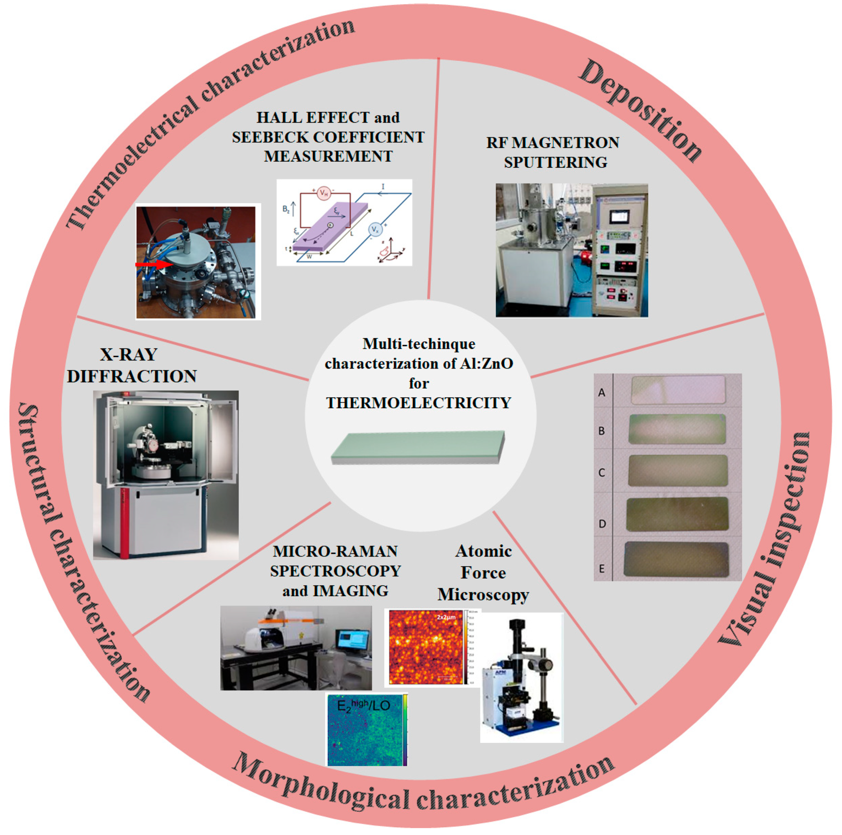
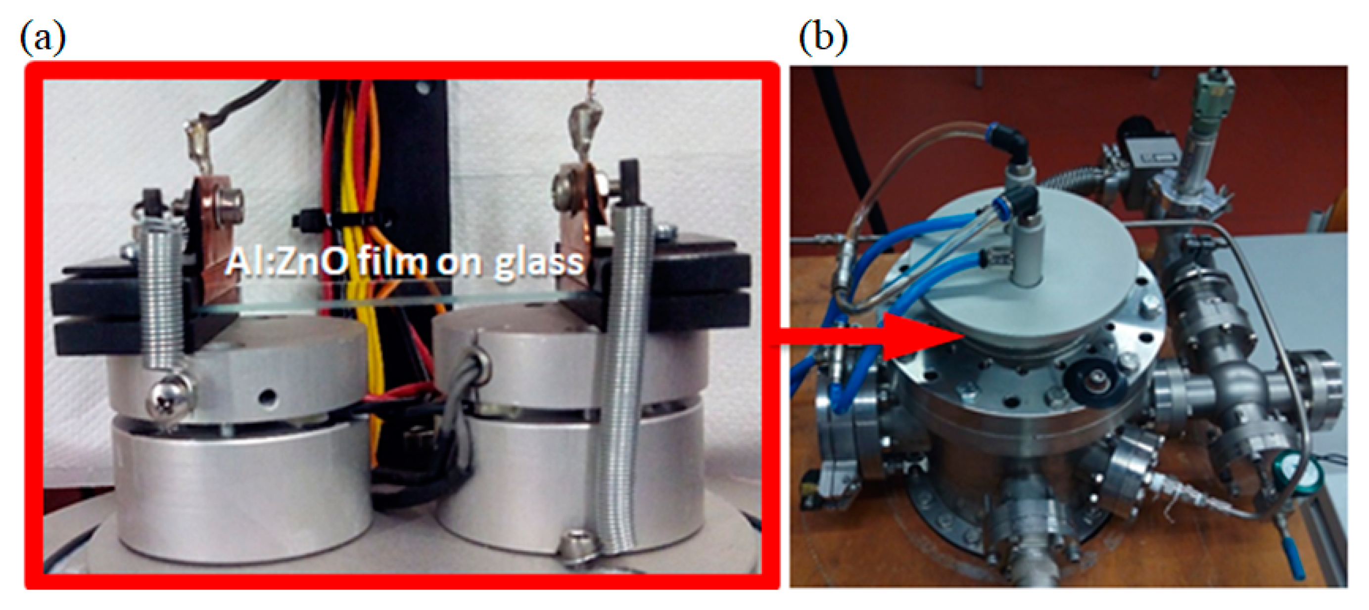
2. Materials and Methods

Five samples of Al:ZnO (AZO) thin films, with an Al doping concentration ranging from 2 to 8 at.%., were deposited onto glass substrates (standard microscope slides) using magnetron sputtering. Prior to deposition, the substrates were cleaned in acetone and ethanol to remove the surface impurities. To prepare the AZO films, an RF power of 120 W was regulated to a ZnO 3” target with a purity of 99.99%, while a DC power ranging from 20 to 60 W was used to regulate an Al 3” target with a purity of 99.99%. This allowed to control the Al dopant concentration in the films. The film thickness was probed to be 300 ± 5 nm for all the samples, using a conventional stylus profilometer. Two nominally identical replicas of each of the five samples were also deposited in order to verify the results. The samples were labeled as sample A, B, C, D, and E corresponding throughout this manuscript to an atomic percent (at.%) doping of 2, 3, 4, 5, and 8, respectively. The dopant concentration was previously calibrated by Energy Dispersive X-ray Spectroscopy (EDX), performed on the film surface using a FEI Quanta-200 ESEM.
The structural and morphological characterizations of the samples were carried out using X-ray diffraction (PanAnalytical X’Pert Pro diffractometer), micro-Raman spectroscopy, and Atomic Force Microscopy (AFM). An ambient pressure NTEGRA AURA NT-MDT AFM microscope was used to investigate the topography of the AZO thin films. The AFM images were acquired in semi-contact (tapping) mode in air, under ambient conditions, using commercially available rectangular-shaped silicon cantilevers (MikroMaschHQ: CSC37/NoAl) with nominal elastic constants between 0.2 and 0.8 N m−1 and a resonance frequency between 20 and 40 KHz. The average roughness (Sa) and Root Mean Square (RMS) roughness (Sq) were obtained by using the free software Gwyddion (v. 2.41). Raman spectroscopy was performed using a Renishaw InVia micro-spectrometer equipped with a solid-state laser centered at 532 nm. Single spectra were recorded on the sample using a Gaussian beam focused onto the surface to about 1.5 µm of FWHM and a fluence of 11 mJ/µm2. Maps were recorded in the streamline mode, letting the laser beam pass through a cylindrical lens in order to become line-shaped. The line had an FWHM of about 3.2 µm and a linear extension of 65 µm. The laser fluence in this mode was about 1 mJ/µm2.
The electronic transport characterization was addressed resorting to a two-fold approach: Hall probes were realized in van der Pauw geometry to measure the carrier density and Hall mobility, while the electrical conductivity was also probed resorting to the homemade setup engineered for the measurement of the Seebeck coefficient. The Seebeck coefficient of the investigated samples was determined using custom-made equipment operated in low vacuum conditions (1 Pa). The equipment consisted of two Peltier devices (Quick-Ohm Küpper & Co. GmbH) used for heating and cooling the edges of a 25 × 75 mm2 sample area. A dedicated electrical circuit specifically designed for measuring the Seebeck voltage generated in the sample was exploited, in response to a thermal gradient across the film surface. The stability of heating and cooling was controlled through custom-developed software and hardware. The Seebeck coefficient was estimated using the formula S = ∆V/∆T, where ∆T is the temperature difference between the edges of the film and ∆V is the corresponding measured potential difference, or thermovoltage. The latter was measured for different thermal gradients applied to the film deposited onto a glass slide. In particular, two separate measurement campaigns were carried out, exploring the ∆T range 35–60 °C and 15–70 °C, respectively. The obtained ∆V values were plotted against the thermal gradient, ∆T, and a linear fit was performed. The Seebeck coefficients were determined as the slope of the fitting curves.
A Multitechnique Approach to the Study of Thermoelectric Metal:ZnO Thin Films
Figure 1 provides a diagrammatic representation of the experimental techniques employed in this work for the comprehensive investigation of the structural, morphological, electrical, and thermoelectric properties of AZO thin films. The diagram is divided into five clockwise oriented slides, highlighting the main techniques and methods used, ranging from the sample growth to the thermoelectric measurement. The RF magnetron sputtering (1st slice) was used to deposit five AZO thin films, each with a thickness of 300 nm, onto glass substrates, with an Al doping level in the range of 2–8 at.%, along with five identical replicas of each sample. The 2nd slice provides a photograph of the sample. Table 1 lists the samples that were grown for this study. Each sample was measured following a specific protocol, including AFM and micro-Raman imaging to assess the morphological homogeneity, surface structure, and quality of the film (3rd slice), XRD and Raman spectroscopy to identify the main crystalline phases and structures, as well as phonon modes (4th slice), and finally electrical transport measurement (Hall effect) and thermoelectric measurements to estimate the carrier density and mobility, and the Seebeck coefficients (5th slice).
Figure 2a,b reports two photographs of the homemade experimental setup used for the Seebeck coefficient measurement. The system was developed for the purpose of accessing the thermoelectric parameters of thin films deposited onto large-area substrates. The thin films’ samples deposited onto glass substrates were mechanically clamped and electrically contacted at both ends. The setup allowed for the application of a controlled temperature difference between the two ends of the sample, creating a temperature gradient across the thin film. This gradient drove the Seebeck effect, causing the charge carriers to diffuse from the hot to the cold side of the film, resulting a voltage difference between the two ends, namely, the thermovoltage. The measurement of the thermovoltage provided a direct measure of the Seebeck coefficient.

3. Results and Discussion

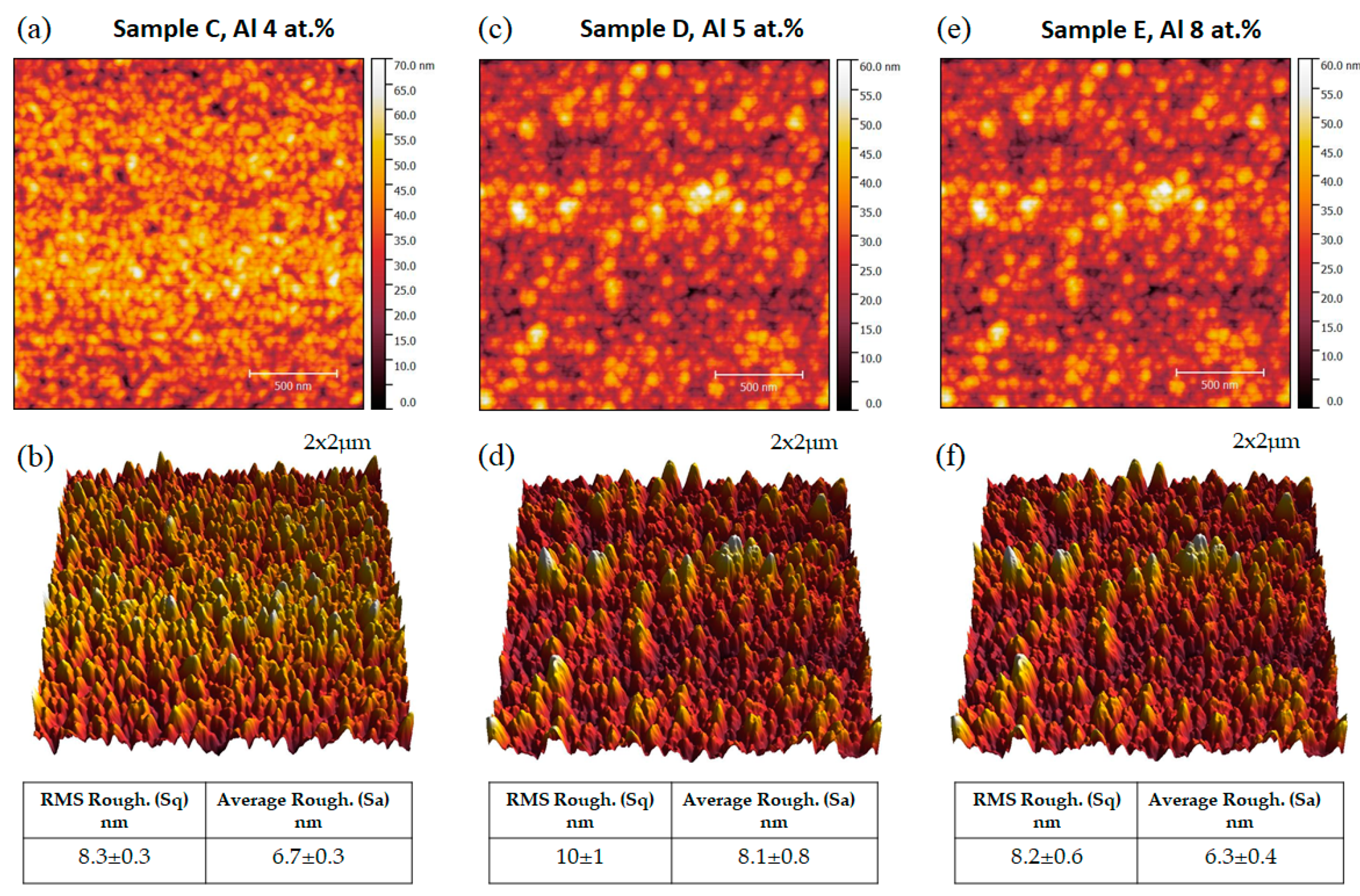
3.1. Visual Inspection and Topographical Characterization Using AFM

In Figure 1, the slice “Visual inspection” displays a photograph of the set of five samples, labeled with capital letters from A to E corresponding to the nominal Al concentrations ranging from 2–8 at.% (as summarized in Table 1). The different colors of the samples reflected the different Al contents, while the film thickness remained constant at 300 nm across the entire set. In Figure 3, the results of the AFM study carried out on the samples with Al doping concentrations of 4 at.%, 5 at.%, and 8 at.% are shown. The films’ surface topography and roughness—both root mean square and mean roughness—were investigated. The AFM images reveal the films’ homogeneous topography, with a grain size in the range of a few tens of nanometers. In particular, the high-resolution images show a grain diameter size around 60 nm. The mean average roughness (Sa) measured in several different regions of the films did not exceed 10 nm. Although the imaging was acquired in air, no physiosorbed structures were observed on the surface resulting in an extremely stable system where the tip did not drag any external structure.

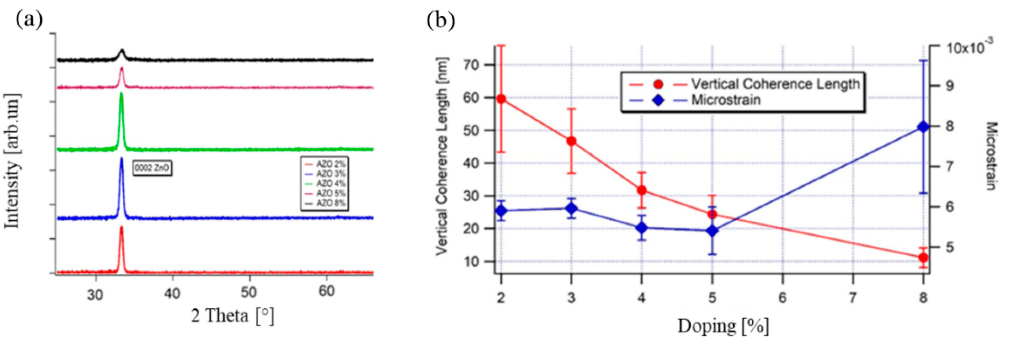
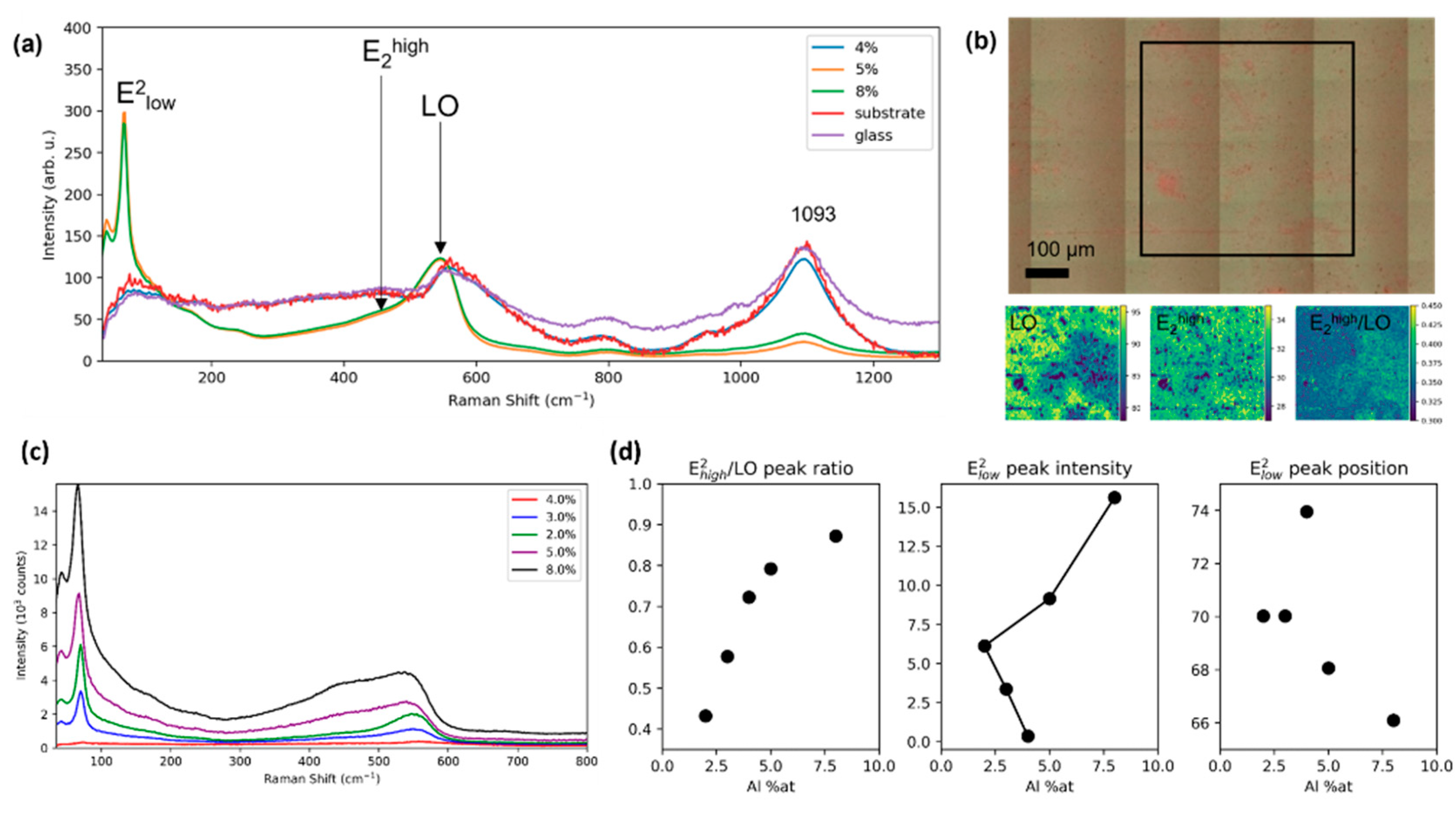
3.2. Structural and Compositional Characterization with XRD and Uraman

High Resolution X-Ray Diffraction (HRXRD) spectroscopy measurements were performed in a parallel beam geometry using a Göebel mirror in the incidence optics in order to obtain a parallel X-ray beam. The detection optics were comprised of a 0.27° parallel plates collimator, a flat graphite monochromator, and a single point gas proportional detector. Figure 4a reports the results of 2θ−θ scans. The only peaks ascribable to ZnO were those identified as ZnO (0002), strong and dominant, and ZnO (0004), weak and satellite. This demonstrates the strong preferential c-axis orientation of the AZO grains, i.e., the c-axis was perpendicular to the sample surface, as previously reported for different substrates [33,34]. The intensity of both the main and satellite peaks decreased as the Al doping concentration increased from 2 at.% to 8 at.%, with the ZnO (0004) peak fully vanishing in the 8 at.% Al-doped sample. Overall, this implies that the degree of crystalline orientation also decreased with the doping concentration. Focusing on the main ZnO (0002) peak, for all the samples, the peak position was between 33.30° and 33.34°, displaying a shift towards the lower angles with respect to the position of the corresponding peak for the bulk ZnO, typically around 32.42° [PDF 00-036-1451] [35]. Notably, this suggests the occurrence of tensile stress along the c-axis direction. Since the observed band shift was not dependent on the Al doping level, it was tentatively ascribed to the presence of the substrate. In order to retrieve quantitative information on the microstructure of the AZO thin films, the ZnO (0002) peak was analyzed using the single line method, based on the fitting of a single diffraction peak with the Voigt function, separating the Lorentzian contribution from the Gaussian one, following the approach proposed by De Keijser [36,37]. In this framework, the Lorentzian broadening was associated with the coherence length of the films, defined as the average extension of the crystal lattice regions that scattered coherently, i.e., those regions that were free of macroscopical defects such as grain boundaries or dislocations. The Gaussian component was linked to the broadening due to the microstrain, i.e., the lattice strain from displacements of the unit cells about their lattice positions due to the defects [38,39]. Analyzing the broadening of the 2θ−θ peaks, the coherence length along the normal direction to the surface (vertical coherence length Lz) and the microstrain ε could be extracted. This approach is based on the Scherrer formula [37,38,39] for the coherence length, which is defined as Lz = Kλ/(βLcos(θ)). Here, K is the shape factor, which is usually taken to be 0.9, λ is the X-ray wavelength, and β represents the integral breadth. β is marked as βG when it is the Gaussian integral breadth, and as βL when it is the Lorentzian one. The microstrain ε is obtained via the Wilson–Stokes formula, ε = βG/[4tan(θ)] [37,38,39]. The results of this analysis are reported in Figure 4b, where it was observed that the vertical coherence length decreased as the doping concentration was increased. The results show that increasing the Al dopant concentration and going over the limit of solubility, which is around 4 at.% [34], the Al interstitial concentration increased and so did the strain in the matrix, determining a lowering of the crystal quality [33]. In fact, concentrations of Al above the limit of solubility likely promoted the formation of inclusions and clusters, which compromised the crystalline quality. The extracted parameters are summarized in Table 2.
Raman spectroscopy provides an extremely versatile, contactless tool for the quantitative investigation of advanced functional materials, ranging from bulky materials [40] to nanostructures and low-dimensional systems, including nanotubes [41], 2D materials [42], and topological materials [43]. Figure 5 presents the results of the Raman analysis carried out on the AZO thin films. Panel (a) shows the spectra of the sample, extracted as the average of all the spectra collected on a spatial map, as shown in panel (b). The same graph also includes the Raman spectrum obtained by measuring the bare substrate of the AZO film (red line) and a spectrum recorded on a commercial microscopy silica glass. This allowed for the band observed around 1093 cm−1 to be attributed to the glass substrate. Similarly, the skew band that peaked at 560 cm−1 was also assigned to the substrate. The ZnO vibrational features were identified through the E2low peak, E2high peak, and the LO band, as highlighted in the panel. Panel (b) shows an optical image of the sample with a dopant concentration of 8 at.%. On the region delimited by the black square in the top of panel (b), the intensity of the LO band, the E2high peak, and the E2high/LO ratio are shown in the bottom part of the panel from left to right, respectively. Notably we did not observe any relevant peak related to the formation of ZnO2, previously reported around 838 and 936 cm−1 [44]. Other than some spot-like defect, the sample appeared to be essentially homogeneous, as testified by the E2high intensity map. The LO band was clearly influenced by the contribution arising from the substrate. Therefore, the variation in intensity of the LO band might have been ascribed to a small local variation in the film thickness, as they were not reflected by the behavior of the E2high peak. In panel (c), single Raman spectra recorded on each of the five samples are shown. The spectra were recorded in the same experimental conditions (see Section 2) and thus displayed the intensities as recorded. In order to highlight the dependence of the spectral features on doping, panel (d) plots the trend of the E2high/LO ratio, the E2low intensity, and the E2low peak position. In fact, these two peaks were related to the ZnO vibrational modes [45] and their relative change could be used as a fingerprint for the presence of substitutional dopants [46]. The observed E2high/LO dependency on doping was in good agreement with the conductivity measured in the sample and with the results previously reported in the literature [47]. It is worth noting that, with respect to the existing literature, the Raman shift assigned to the E2low peak was about 30 cm−1 lower, as it was typically reported to be about 100 cm−1 [48,49]. This could be related to the substitution of zinc atoms with aluminum in the crystal lattice [49].

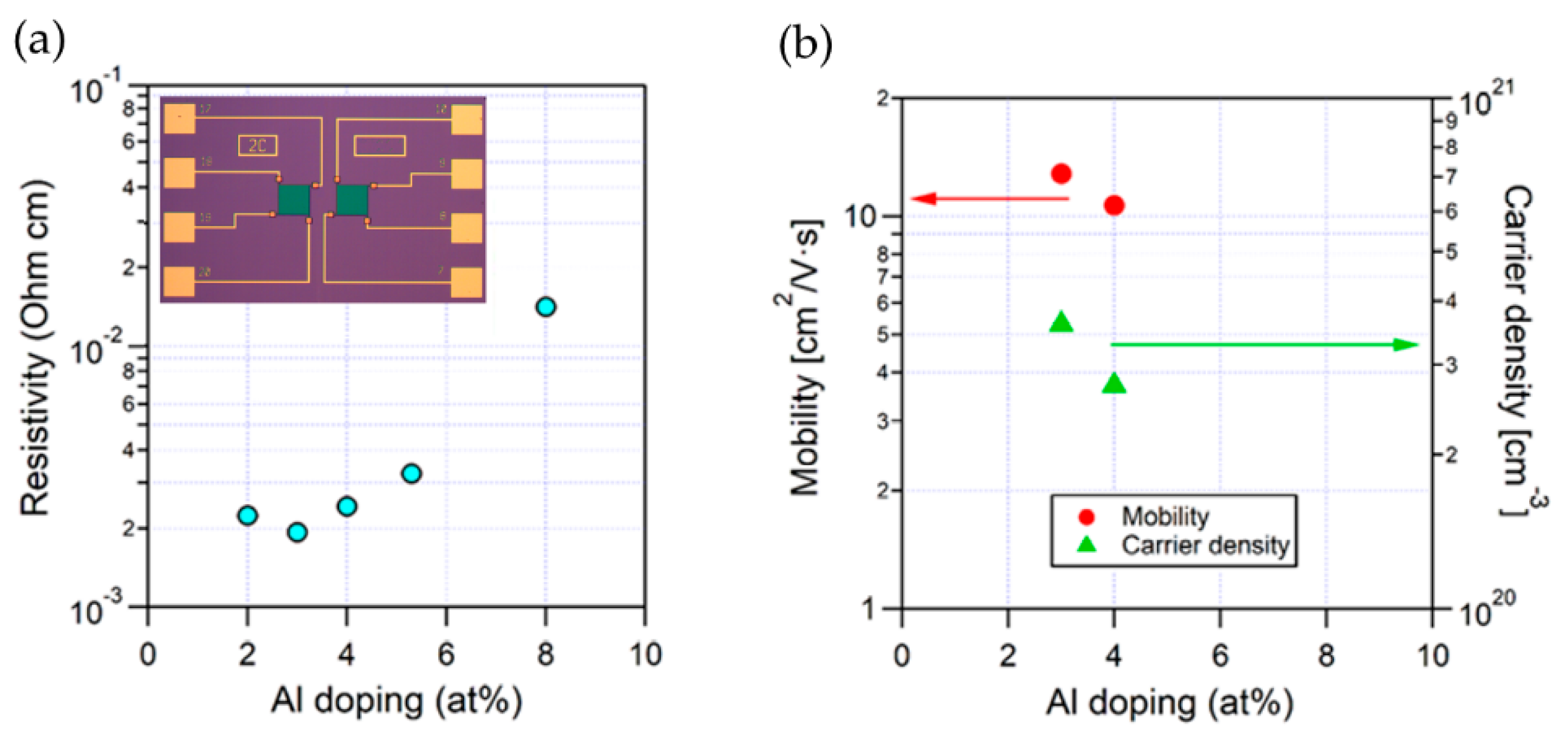
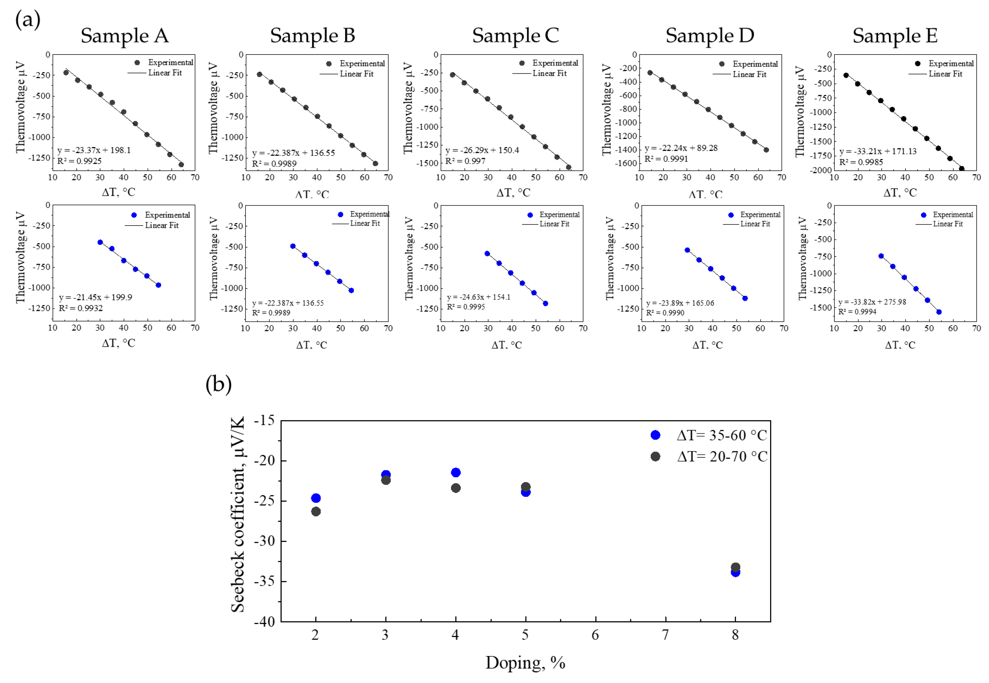
3.3. Electrical and Thermoelectric Transport

The results of the electrical transport measurements are reported in Figure 6. The left panel shows the electrical resistivity of all samples as a function of the Al content. Overall, the set of samples displayed a spread in the resistivity of about one order of magnitude, with the minimum (2 × 10⁻³ Ohm·cm) and maximum (2 × 10⁻² Ohm·cm) values achieved at 3 at.% and 8 at.% doping, respectively. The sample with 3 at.% Al doping exhibited the highest value for both the mobility (above 10 cm2 V−1 s−1) and carrier density (around 4 × 1021 cm−3) (Figure 6b). This was consistent with the experimental evidence of the lowest resistivity as reported in the left panel.
Figure 7 reports the thermoelectric characterization of the samples, using the homemade experimental setup described in Figure 2. The thermovoltage of each sample was measured twice by varying the thermal gradient in two different ranges. The ten small panels in Figure 7a show, for all the samples, the thermovoltage plotted against the applied thermal gradients in the range 15–70 °C (top graph) and in the range 30–60 °C (bottom graph). The graphs display both the experimental data and the linear fit, where the slope of the fitting line represents the Seebeck coefficient. In Figure 7b the extracted Seebeck coefficient of samples A–E is plotted as a function of the Al amount in the samples. The two datasets (dark and blue dots) represented the results obtained in the two ranges of the applied thermal gradients, and they were in very good agreement. The values of the Seebeck coefficients were in the range of 22–33 µV/K, exhibiting a broad minimum at intermediate doping levels (3–4 at.%) as well as a relatively high absolute value of the at high doping (8 at.%). On the one hand, the investigated thermoelectric features of the measured samples were shown to be relatively stable and robust against changes in the doping level of almost one order of magnitude. On the other hand, the significant thermovoltage observed for the high doping regime suggested possible routes for applications such as temperature and thermal sensing, where the focus is on the response to a change in the temperature rather than on the generation of power.

4. Conclusions

In the context of using nanomaterials for sustainable energy harvesting and conversion, a multi-technique investigation was conducted on a set of 300-nm-thick Al-doped ZnO thin films (2–8 at.% doping) as potential candidates for highly efficient thermoelectric applications. The samples were designed and deposited using magnetron sputtering. The study involved a comprehensive analysis of the structural, morphological, electrical, and thermoelectrical properties of the samples using various experimental techniques. AFM was used to test the sample topography and surface homogeneity, while XRD was used to identify the main crystal phases. This study shows that the films had a homogeneous topography, with a grain size in the range of a few tens of nanometers, and that increasing the Al doping concentration decreased the crystalline quality, especially for a doping level exceeding 4 at.%, corresponding to the solubility limit of Al in ZnO. The presence of substitutional dopants was confirmed by the micro-Raman study. Electrical transport was studied by means of devices shaped in Hall bar geometry, while thermoelectric transport was measured using a homemade setup for the measurement of the Seebeck coefficient. The structure–property relationship of the samples was assessed by analyzing the exhibited trends as a function of the Al doping concentration. ZnO films with a 3–4 Al at.% exhibited the lowest absolute value of the Seebeck coefficient, while those with an 8 Al at.% had the highest. Within the almost one order of magnitude of the doping level considered in this work, the thermoelectric features of the investigated samples were found to be relatively stable and did not display abrupt changes. Overall, the study’s protocol and results are of interest for large-scale application systems, and the relatively high thermovoltage response reported at high doping opens the way for thermal sensing applications.

Author Contributions

Conceptualization, F.R. and C.J.T.; methodology, F.R., C.J.T. and S.B.; validation, formal analysis and investigation, M.I., V.D., S.B. and A.d.B.; resources, F.R.; data curation and writing—original draft preparation, M.I., F.R. and V.D.; writing—review and editing, M.I, R.M.M., V.D., L.M., S.F., C.C. V.B., A.M., G.P., A.R., S.B., A.d.B., J.M.R., C.J.T. and F.R.; supervision, F.R. All authors have read and agreed to the published version of the manuscript.

Funding

This research was funded by MIUR-PON, scholarship PhD program “Physics and nano sciences” 2021/22.“Nanotecnologie per la termoelettricità e l’energy harvesting” (Azione IV.5 “Dottorati su tematiche green”) and by project QUANTEP, INFN CSN5. VB was supported by the project “Brosynano”MICINN-FEDER (PID2019-106820RB-C22). C.T. acknowledges the funding from FCT/PIDDAC through the Strategic Funds project reference UIDB/04650/2020-2023. A.M., G.P. acknowledge support by the Italian Ministry of University and Research through PRIN UTFROM N. 20178PZCB5. This work was also partially funded under the National Recovery and Resilience Plan (NRRP), Mission 04 Component 2 Investment 1.5 – NextGenerationEU, Call for tender n. 3277 dated 30/12/2021. Award Number: 0001052 dated 23/06/2022.

Institutional Review Board Statement

Not applicable.

Informed Consent Statement

Not applicable.

Data Availability Statement

The data presented in this study are available on request from the corresponding author.

Conflicts of Interest

The authors declare no conflict of interest.

References

  1. Dresselhaus, M.; Chen, G.; Tang, M.; Yang, R.; Lee, H.; Wang, D.; Ren, Z.; Fleurial, J.-P.; Gogna, P. New Directions for Low-Dimensional Thermoelectric Materials. Adv. Mater. 2007, 19, 1043–1053. [Google Scholar] [CrossRef]
  2. Chen, R.; Lee, J.; Lee, W.; Li, D. Thermoelectrics of Nanowires. Chem. Rev. 2019, 119, 9260–9302. [Google Scholar] [CrossRef] [PubMed]
  3. Prete, D.; Dimaggio, E.; Demontis, V.; Zannier, V.; Rodriguez-Douton, M.J.; Guazzelli, L.; Beltram, F.; Sorba, L.; Pennelli, G.; Rossella, F. Electrostatic Control of the Thermoelectric Figure of Merit in Ion-Gated Nanotransistors. Adv. Funct. Mater. 2021, 31, 2104175. [Google Scholar] [CrossRef]
  4. Rocci, M.; Demontis, V.; Prete, D.; Ercolani, D.; Sorba, L.; Beltram, F.; Pennelli, G.; Roddaro, S.; Rossella, F. Suspended InAs Nanowire-Based Devices for Thermal Conductivity Measurement Using the 3ω Method. J. Mater. Eng. Perform. 2018, 27, 6299–6305. [Google Scholar] [CrossRef]
  5. Rossella, F.; Pennelli, G.; Roddaro, S. Chapter Six—Measurement of the thermoelectric properties of individual nanostructures, Part of volume: Nanowires for Energy Applications, Edited by Sudha Mokkapati, Chennupati Jagadish. Semicond. Semimet. 2018, 98, 409–444. [Google Scholar]
  6. Biswas, K.; He, J.; Blum, I.; Wu, C.I.; Hogan, T.P.; Seidman, D.N.; Dravid, V.P.; Kanatzidis, M.G. High-performance bulk thermoelectrics with all-scale hierarchical architectures. Nature 2012, 489, 414–418. [Google Scholar] [CrossRef]
  7. Peri, L.; Prete, D.; Demontis, V.; Zannier, V.; Rossi, F.; Sorba, L.; Beltram, F.; Rossella, F. Giant reduction of thermal conductivity in twinning superlattice InAsSb nanowires. Nano Energy 2022, 103, 107782. [Google Scholar] [CrossRef]
  8. Maldovan, M. Phonon wave interference and thermal bandgap materials. Nat. Mater 2015, 14, 667–674. [Google Scholar] [CrossRef] [PubMed]
  9. Jeong, C.; Datta, S.; Lundstrom, M. Thermal conductivity of bulk and thin-film silicon: A Landauer approach. J. Appl. Phys. 2012, 111, 93708. [Google Scholar] [CrossRef] [Green Version]
  10. DeCoster, M.E.; Chen, X.; Zhang, K.; Rost, C.M.; Hoglund, E.R.; Howe, J.M.; Beechem, T.E.; Baumgart, H.; Hopkins, P.E. Thermal Conductivity and Phonon Scattering Processes of ALD Grown PbTe–PbSe Thermoelectric Thin Films. Adv. Funct. Mater. 2019, 29, 1904073. [Google Scholar] [CrossRef]
  11. Latronico, G.; Singh, S.; Mele, P.; Darwish, A.; Sarkisov, S.; Pan, S.W.; Kawamura, Y.; Sekine, C.; Baba, T.; Mori, T.; et al. Synthesis and Characterization of Al-and SnO2-Doped ZnO Thermoelectric Thin Films. Materials 2021, 14, 6929. [Google Scholar] [CrossRef] [PubMed]
  12. Trinh, T.Q.; Nguyen, T.T.; Vu, D.V.; Le, D.H. Structural and thermoelectric properties of Al-doped ZnO thin films grown by chemical and physical methods. J Mater Sci. Mater Electron 2017, 28, 236–240. [Google Scholar] [CrossRef]
  13. Janotti, A.; Van de Walle, C.G. Fundamentals of zinc oxide as a semiconductor. Rep. Prog. Phys. 2009, 7, 126501. [Google Scholar] [CrossRef] [Green Version]
  14. Ozgur, U.; Alivov, Y.I.; Liu, C.; Teke, A.; Reshchikov, M.A.; Dogan, S.; Cho, S.J.; Morkoc, H.J. A comprehensive review of ZnO materials and devices. Appl. Phys. 2005, 98, 041301. [Google Scholar]
  15. Xu, Y.; Goto, M.; Kato, R.; Tanaka, Y.; Kagawa, Y. Thermal conductivity of ZnO thin film produced by reactive sputtering. J. Appl. Phys. 2012, 111, 84320. [Google Scholar] [CrossRef]
  16. Ellmer, K.; Klein, A.; Rech, B. Transparent Conductive Zinc Oxide: Basics and Applications in Thin Film Solar Cells; Springer Science & Business Media: Berlin, Germany, 2007; 29 dic. [Google Scholar]
  17. Demontis, V.; Sanna, C.; Melskens, J.; Santbergen, R.; Smets, A.H.M.; Damiano, A.; Zeman, M. The role of oxide interlayers in back reflector configurations for amorphous silicon solar cells. J. Appl. Phys. 2013, 113, 64508. [Google Scholar] [CrossRef] [Green Version]
  18. Wang, L.; Zhang, G.; Liu, Q.; Duan, H. Recent progress in Zn-based anodes for advanced lithium ion batteries. Mater. Chem. Front. 2018, 2, 1414–1435. [Google Scholar] [CrossRef]
  19. Zhang, J.; Gu, P.; Xu, J.; Xue, H.; Pang, H. High performance of electrochemical lithium storage batteries: ZnO-based nanomaterials for lithium-ion and lithium–sulfur batteries. Nanoscale 2016, 8, 18578. [Google Scholar] [CrossRef] [PubMed]
  20. Ong, C.B.; Ng, L.Y.; Mohammad, A.W. A review of ZnO nanoparticles as solar photocatalysts: Synthesis, mechanisms and applications. Renew. Sustain. Energy Rev. 2018, 81, 536–551. [Google Scholar] [CrossRef]
  21. Wang, Z.L.; Song, J. Piezoelectric Nanogenerators Based on Zinc Oxide Nanowire Arrays. SCIENCE 2006, 312, 242–246. [Google Scholar] [CrossRef]
  22. Chubenko, E.; Alhamd, M.W.; Bondarenko, V. Optical properties of hydrothermally deposited Ni and Co doped nanostructured ZnO thin films as scintillating coatings for beta-particles detection. J. Lumin. 2022, 247, 118860. [Google Scholar] [CrossRef]
  23. Uklein, A.V.; Multian, V.V.; Kuz'micheva, G.M.; Linnik, R.P.; Lisnyak, V.V.; Popov, A.I.; Gayvoronsky, V.Y. Nonlinear optical response of bulk ZnO crystals with different content of intrinsic defects. Opt. Mater. 2018, 84, 738–747. [Google Scholar] [CrossRef]
  24. Singh, P.; Kumar, R.; Singh, R.K. Progress on Transition Metal-Doped ZnO Nanoparticles and Its Application. Ind. Eng. Chem. Res. 2019, 58, 17130–17163. [Google Scholar] [CrossRef]
  25. Pan, Z.; Tian, X.; Wu, S.; Xiao, C.; Li, Z.; Deng, J.; Hu, G.; Wei, Z. Effects of Al and Sn dopants on the structural and optical properties of ZnO thin films. Superlattices Microstruct 2013, 54, 107–117. [Google Scholar] [CrossRef]
  26. Gupta, A.; Kumar, S.; Jindal, K.; Sharma, A.; Tomar, M. Enhanced Low Temperature Thermoelectric Properties by Nano-Inclusion of 2D MoS2 with Fe:ZnO Thin Films. J. Electron. Mater. 2021, 50, 4567–4576. [Google Scholar] [CrossRef]
  27. Patel, P.B.; Panchal, C.; Desai, M.S.; Ray, J. Magnetron Sputtered Al-ZnO Thin Films for Photovoltaic Applications. J. Nano- Electron. Phys. 2011, 3, 755. [Google Scholar]
  28. Pandey, R.K.; Mishra, S.; Bajpai, P.K. Deposition and Characterization of Al:ZnO Thin Films for Optoelectronic Applications. J. Electron. Mater. 2016, 45, 5822–5829. [Google Scholar] [CrossRef]
  29. Dasgupta, N.P.; Neubert, S.; Lee, W.; Trejo, O.; Lee, J.R.; Prinz, F.B. Atomic Layer Deposition of Al-doped ZnO Films: Effect of Grain Orientation on Conductivity. Chem. Mater. 2010, 22, 4769–4775. [Google Scholar] [CrossRef]
  30. Alam, M.W.; Ansari, M.Z.; Aamir, M.; Waheed-Ur-Rehman, M.; Parveen, N.; Ansari, S.A. Preparation and Characterization of Cu and Al Doped ZnO Thin Films for Solar Cell Applications. Crystals 2022, 12, 128. [Google Scholar] [CrossRef]
  31. Isotta, E.; Andrade-Arvizu, J.; Syafiq, U.; Jiménez-Arguijo, A.; Navarro-Güell, A.; Guc, M.; Saucedo, E.; Scardi, P. Towards Low Cost and Sustainable Thin Film Thermoelectric Devices Based on Quaternary Chalcogenides. Adv. Funct. Mater. 2022, 32, 2202157. [Google Scholar] [CrossRef]
  32. Viet Vu, D.; Hai Le, D.; Xuan Nguyen, C.; Quang Trinh, T. Comparison of structural and electric properties of ZnO-based n-type thin films with different dopants for thermoelectric applications. J Sol-Gel Sci Technol 2019, 91, 146–153. [Google Scholar] [CrossRef]
  33. Valenti, I.; Benedetti, S.; di Bona, A.; Lollobrigida, V.; Perucchi, A.; Di Pietro, P.; Lupi, S.; Valeri, S.; Torelli, P. Electrical, optical, and electronic properties of Al:ZnO films in a wide doping range. J. Appl. Phys. 2015, 118, 165304. [Google Scholar] [CrossRef]
  34. Matsubara, K.; Fons, P.; Yamada, A.; Watanabe, M.; Niki, S. Epitaxial growth of ZnO thin films on LiNbO3 substrates. Thin Solid Film. 1999, 347, 238–240. [Google Scholar] [CrossRef]
  35. McMurdie, F.; Morris, M.C.; Evans, E.H.; Paretzkin, B.; Wong-Ng, W.; Ettlinger, L.; Hubbard, C.R. Standard X-ray diffraction powder patterns from the JCPDS research associateship. Powder Diffr. 1986, 1, 76. [Google Scholar] [CrossRef]
  36. De Keijser, T.H.; Langford, J.I.; Mittemeijer, E.J.; Vogels, A.B.P. Use of the Voigt function in a single-line method for the analysis of X-ray diffraction line broadening. J. Appl. Cryst. 1982, 15, 308. [Google Scholar] [CrossRef]
  37. Delhez, R.; de Keijser, T.H.; Mittemeijer, E.J. Determination of crystallite size and lattice distortions through X-ray diffraction line profile analysis, Z. Anal. Chem. 1982, 312, 1–16. [Google Scholar] [CrossRef]
  38. Metzger, T.; Höpler, R.; Born, E.; Ambacher, O.; Stutzmann, M.; Stömmer, R.; Schuster, M.; Göbel, H.; Christiansen, S.; Albrecht, M.; et al. Defect structure of epitaxial GaN films determined by transmission electron microscopy and triple-axis X-ray diffractometry. Philos. Mag. A 1998, 77, 1013–1025. [Google Scholar] [CrossRef]
  39. Chierchia, R.; Böttcher, T.; Heinke, H.; Einfeldt, S.; Figge, S.; Hommel, D. Microstructure of heteroepitaxial GaN revealed by x-ray diffraction. J. Appl. Phys. 2003, 93, 8918. [Google Scholar] [CrossRef]
  40. Galinetto, P.; Rossella, F.; Minzioni, P.; Razzari, L.; Cristiani, I.; Degiorgio, V.; Kokanyan, E.P. Microraman and photorefractivity study of hafnium-doped lithium niobate crystals. J. Nonlinear Opt. Phys. Mater. 2006, 15, 9–21. [Google Scholar] [CrossRef]
  41. Bellucci, S.; Chiaretti, M.; Onorato, P.; Rossella, F.; Grandi, M.S.; Galinetto, P.; Sacco, I.; Micciulla, F. Micro-Raman study of the role of sterilization on carbon nanotubes for biomedical applications. Nanomedicine 2010, 5, 209–215. [Google Scholar] [CrossRef]
  42. Caridad, J.M.; Rossella, F.; Bellani, V.; Grandi, M.S.; Diez, E. Automated detection and characterization of graphene and few-layer graphite via Raman spectroscopy. J. Raman Spectrosc. 2011, 42, 286–293. [Google Scholar] [CrossRef]
  43. Mehdipour, S.; López, D.; Velázquez, M.; Hidalgo, P.; Méndez, B.; Luna, M.; Bellani, V.; Amado, M.; Balakrishnan, G.; Diez, E. Raman response of topologically protected surface states in sub-micrometric Pb0.77Sn0.23Se flakes. J. Raman Spectr. 2020, 51, 2489. [Google Scholar] [CrossRef]
  44. Bocharov, D.; Chesnokov, A.; Chikvaidze, G.; Gabrusenoks, J.; Ignatans, R.; Kalendarev, R.; Krack, M.; Kundzins, K.; Kuzmin, A.; Mironova-Ulmane, N.; et al. A comprehensive study of structure and properties of nanocrystalline zinc peroxide. J. Phys. Chem. Solids 2022, 160, 110318. [Google Scholar] [CrossRef]
  45. Vinodkumar, R.; Navas, I.; Chalana, S.R.; Gopchandran, K.G.; Ganesan, V.; Philip, R.; Sudheer, S.K.; Pillai, V.M. Highly conductive and transparent laser ablated nanostructured Al: ZnO thin films. Appl. Surf. Sci. 2010, 257, 708–716. [Google Scholar] [CrossRef]
  46. Bundesmann, C.; Ashkenov, N.; Schubert, M.; Spemann, D.; Butz, T.; Kaidashev, E.M.; Lorenz, M.; Grundmann, M. Raman scattering in ZnO thin films doped with Fe, Sb, Al, Ga, and Li. Appl. Phys. Lett. 2003, 83, 1974. [Google Scholar] [CrossRef]
  47. Van Toan, N.; Tuoi, T.T.K.; Inomata, N.; Toda, M.; Ono, T. Aluminum doped zinc oxide deposited by atomic layer deposition and its applications to micro/nano devices. Sci. Rep. 2021, 11, 120. [Google Scholar] [CrossRef]
  48. Sun, M.; Hao, W.; Wang, C.; Wang, T. A simple and green approach for preparation of ZnO2 and ZnO under sunlight irradiation. Chem. Phys. Lett. 2007, 443, 342–346. [Google Scholar] [CrossRef]
  49. Russo, V.; Ghidelli, M.; Gondoni, P.; Casari, C.S.; Li Bassi, A. Multi-wavelength Raman scattering of nanostructured Al-doped zinc oxide. J. Appl. Phys. 2014, 115, 73508. [Google Scholar] [CrossRef] [Green Version]
Figure 1. Sequence of experimental techniques employed in this study for the complete structural, morphological, electronic, and thermoelectric investigation of Al:ZnO thin films: RF magnetron sputtering deposition for the growth of thin films with varying levels of Al doping; optical and morphological investigation by visual inspection; AFM and Raman imaging; structural investigation by XRD and Raman spectroscopy; electronic transport and thermoelectric measurements.
Coatings 13 00691 g001
Figure 2. (a) Core of the homemade setup used for the measurement of the Seebeck coefficient, consisting of two Peltier devices used for heating and cooling the edges of the samples deposited on glass slides. (b) Vacuum chamber, containing the Seebeck measurement setup.
Coatings 13 00691 g002
Figure 3. 2D (panels (a), (c), (e)) and 3D (panels (b), (d), (f)) AFM images, RMS, and average roughness of the AZO thin film with 4 at.%, 5 at.%, and 8 at.% l (samples C, D, and E).
Coatings 13 00691 g003
Figure 4. (a) θ–2θ X-ray diffraction patterns of the AZO films, in accordance with [PDF 00-036-1451]. (b) Vertical coherence length and microstrain in the function of Al-doping (at.%).
Coatings 13 00691 g004
Figure 5. (a) Raman spectra of the AZO samples with doping concentrations of 4 at.%, 5 at.%, and 8 at.% (blue, orange, and green lines), of the substrate (red line) and of another commercial microscopy glass substrate (purple line). The spectra are extracted as the average of all the spectra collected on a spatial map, as the one reported in panel (b). (c) Raman spectra for all the samples, in the 0–800 cm−1 range, where the ZnO vibrational features (E2low peak, E2high, and the LO band) are localized. (d) E2high/LO intensity ratio, E2low peak intensity, and E2low peak spectral position as a function of doping.
Coatings 13 00691 g005
Figure 6. (a) Electrical resistivity of the five samples characterized using a Hall bar device realized by optical lithography (the device architecture is shown in the inset). (b) Carrier mobility and density for the samples with Al doping 3 at.% Al and 4 at.%.
Coatings 13 00691 g006
Figure 7. (a) Thermovoltage plotted against the applied thermal gradients in the range of 15–70 °C (top graph) and in the range of 30–60 °C (bottom graph). The plots show both the experimental data and the linear fit. The slope of the fit represents the Seebeck coefficient, reported in panel (b).
Coatings 13 00691 g007
Table 1. Samples description, Al-doping concentration resulting from the RF sputtering power applied to the Al target. X and X’ are two nominally identical replicas of the same sample.
Sample Name Al (at. %)Al DC Power (W)
A, A’ 220
B, B’330
C, C’440
D, D’550
E, E’860
Table 2. Extracted values of the d-spacing, lattice parameter a, lattice parameter c, vertical coherence length, and microstrain as a function of the doping concentration.
Doping [%]D-Spacing [A]Lattice Parameter a [A]Lattice Parameter c [A]Vertical Coherence Length [nm]Microstrain [× 10−3]
22.68773.29185.375459.6385.9062
32.68723.29115.374346.7395.9646
42.68843.29255.376731.7785.4827
52.68513.28855.370124.3865.4089
82.68553.28915.371111.1457.9833
Disclaimer/Publisher’s Note: The statements, opinions and data contained in all publications are solely those of the individual author(s) and contributor(s) and not of MDPI and/or the editor(s). MDPI and/or the editor(s) disclaim responsibility for any injury to people or property resulting from any ideas, methods, instructions or products referred to in the content.

