3.2.1. UV-Visible Absorption and Transmittance
Once the polymer is doped with PbS NPs, drastic modification in the optical response will occur. Accordingly, optical band gap energy (
) using UV-vis spectroscopy can be measured. Then, based on the molecular orbital theory, one can know how electrons in the π, n, and σ-orbits are promoted from the lower ground level to the higher levels once they absorb the light by incident beam spectral range from ultraviolet to the visible region [
33].
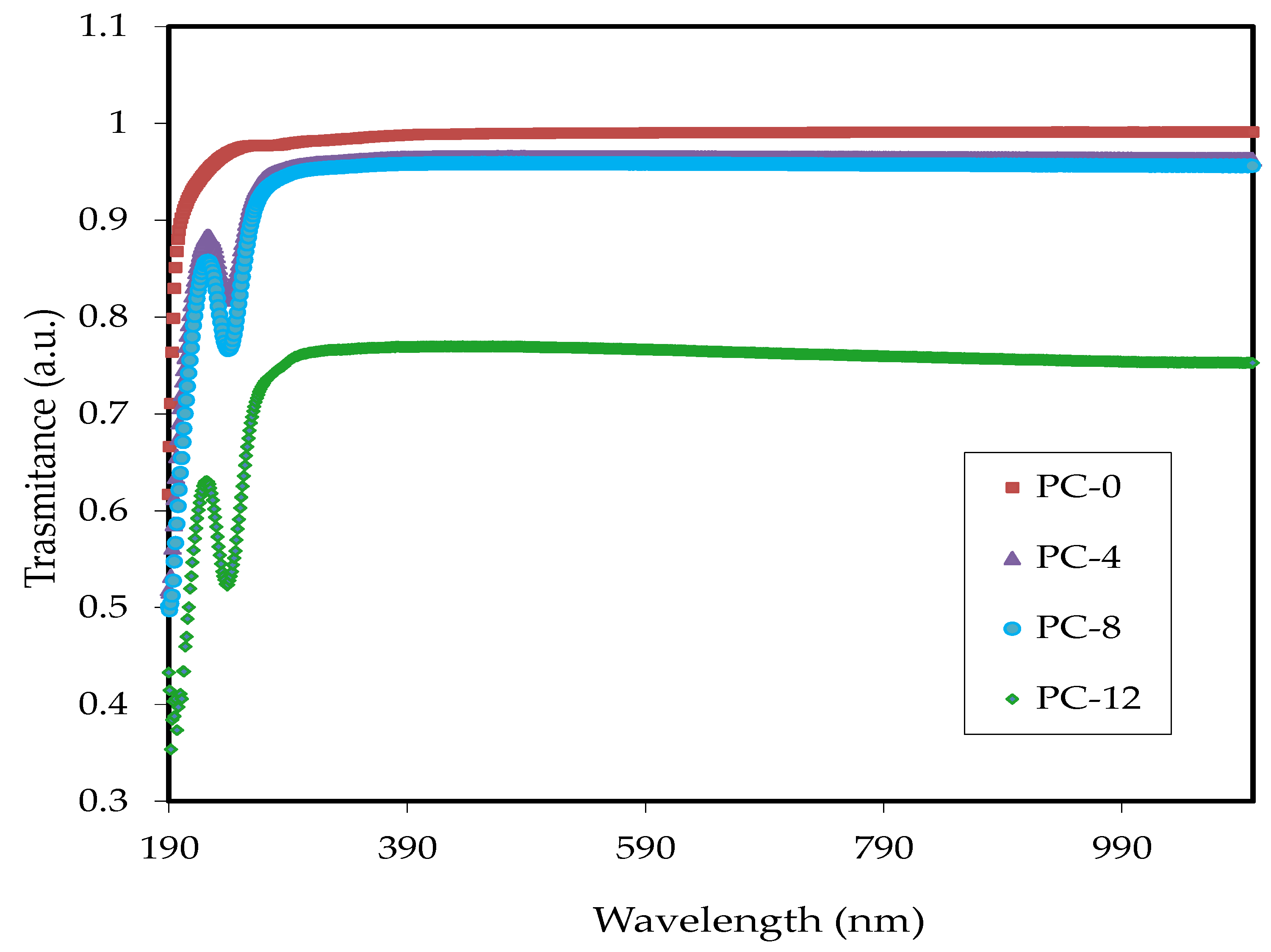
The optical spectra corresponding to PVA and PVA-loaded samples are shown in
Figure 3. The samples have a small absorption in the spectral range from 350 to 800 nm. The only absorption peak at the short UV region is attributed to the absorption of the photon energy that is adequate to interact with atoms of the polymer material, resulting in transferring some electrons from the valance to the conduction band. The incident light transmits completely through the pure PVA. The transmittance decreases as the additive filler amount are increased [
34]. For example, the PVA containing 12 wt% of PbS NPs shows about 74% transparency. This shows that, even though a significant amount of the filler was added to the polymer, the NCPs still have good transparency in the visible region with a strong UV absorption.
In the absorption process, when a sample is illuminated, the amount of light that is transmitted into the system is determined using Equation (2). The absorbance,
A, or quantity of light absorbed can mathematically be shown as follows:
where
Io and
I stand for the initial beam intensity and the intensity of light passing through the sample, respectively [
35,
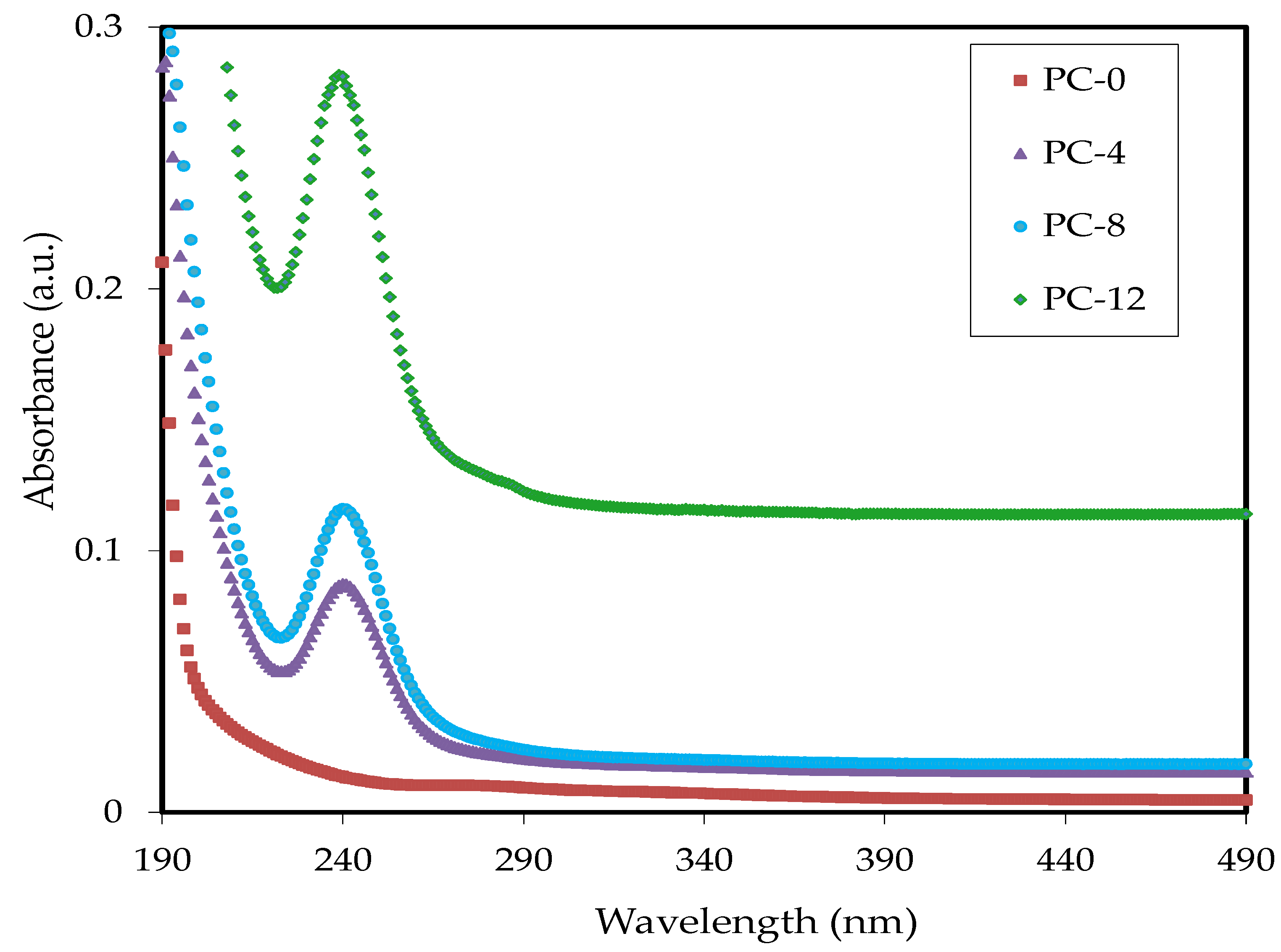
36].The optical absorption spectra corresponding to PVA and PVAs loaded with various PbS NPs over the broadband range from 190 to 900 nm can be manipulated, as shown in
Figure 4. The absorption peaks in the spectra inversely and proportionally change with increasing wavelength and increasing PbS NPs content. The apparent peak that is characteristic appears in the UV region. Remarkably, the doped PVA possesses a tunable UV absorption region. As stated previously, according to the molecular orbital theory, when UV light is absorbed, electrons in the π, σ, and n-orbitals are strongly jumped from the lowest energy state to the higher excited states; therefore, the π → π*, n → π*, and σ → σ* transitions will occur. With those transitions, most optical transitions in the visible region are produced by contaminants.
Figure 4 displays the 240 nm peak caused by n–π* transitions [
37]. The transparency of the samples at relatively higher wavelengths is observed. The spectrum of PVA contains an absorption edge near 210 nm, and the absorption edge of the spectra of all the doped samples slightly shifts towards the longer wavelength. The π → π* transition is an electronic transition which belongs to the conjugated (C=O) group. Moreover, it can be connected to the absorption band in all the systems in the spectral range from 200 to 300 nm. Furthermore, both the non-doped and doped samples had a small absorption band around 330 nm, which is a vibrational feature of PVA. As an interesting phenomenon, the vibronic shoulder appears as the PbS NP concentration increases. This establishes a relationship between the vibronic absorption band and the growth of the crystalline components in the systems. The similar shapes in the absorbance spectra of the PVA:PbS confirm reaching a desired homogeneity throughout the film preparations [
13,
38].
3.2.2. Coefficient of Absorption and Absorption Edge Study
The optical absorption coefficient can determine the material’s ability to absorb light. The analysis of optical properties is a method to determine vibrational energy bands and electron transitions between different energy states [
39].Additionally, a comprehensive understanding of the absorption mechanisms can predict materials’ optically induced crystallinity and non-crystallinity. The extensive examination of the optical property shows developments in the energy band structure modifications. From the analysis of optical absorption spectra taken for the systems, the energy gap (
Eg) is measured. By considering the transmittance and reflectance in the calculation, the following relationship can be used to determine the absorption coefficient (
) [
40]:
where
T,
t,
R, and
α are the transmittance, thickness, reflectance, and absorption coefficient, respectively.
The value of
T is derived from Beer’s law (
). Two main phenomena occur through transmissions: light transmitted by the guiding medium and absorption. The response of a material to the incident light is proportional to the total absorbance of radiation intensity
IA, reflected radiation intensity
IR, and transmitted beam
IT as the radiation passes through the medium, as seen in Equation (4):
The radiation intensity is measured in W m
−2, which describes the total energy transmission per unit of time per area. Equation (4) can also be shown as:
where
R shows reflectivity (
),
A stands for the absorptivity (
), and
T is the transmittivity (
). The other symbols are
T,
A, and
R, representing transmittance, absorbance, and reflectance, respectively. The study of optical absorption shows that the absorption edge as a key factor is used to show the electronic structure of the materials. The occurrence of the indirect and direct transitions inside the bandgap (BG) is clarified from the optical absorption spectra [
40].
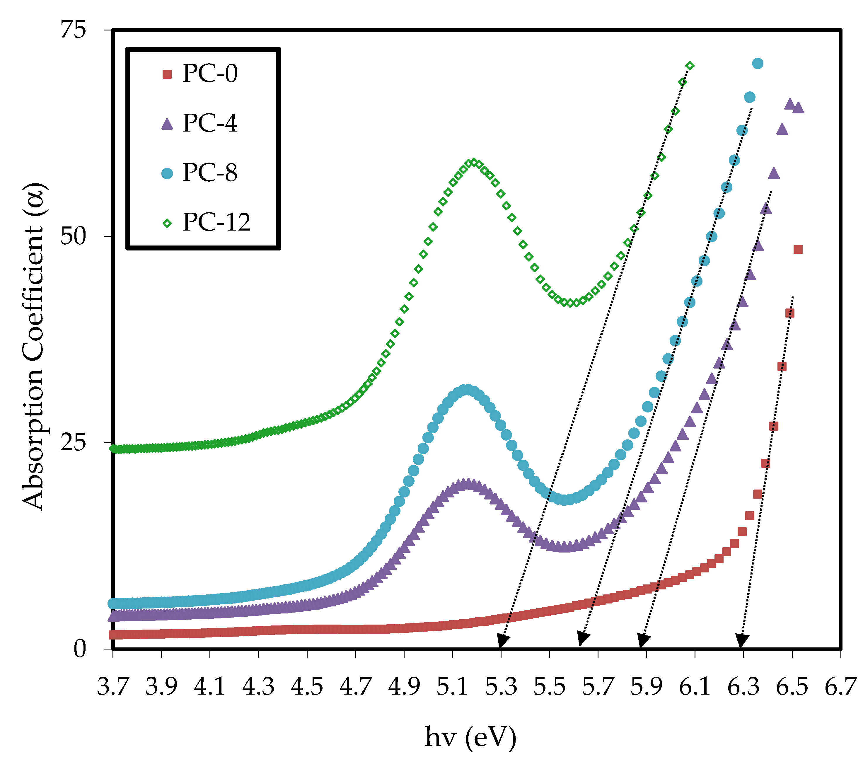
Figure 5 shows the optical coefficient of absorption as a function of the energy of photons of the PVA and PVA:PbS films. Upon the addition of PbS NPs, the absorption edges of PVA shift toward lower photon energy. The shifting is evidence of reducing the optical
Eg due to the additive materials.
Table 2 summarizes the absorption edges measured by extrapolating the linear parts of the absorption coefficient versus photon energy.
Table 2 shows that by increasing the PbS amount, the absorption edge decreased. This decrease occurs due to creating new localized states in the bandgap. In other words, the transition lies below the PVA energy gap and expands the bandgap’s tail. The Urbach tail’s (UT) width measures the degree of disorder in the forbidden gap and the degree of defective levels. The following equation can be used to calculate the UT width [
38]:
where
is a constant and
is the Urbach energy.
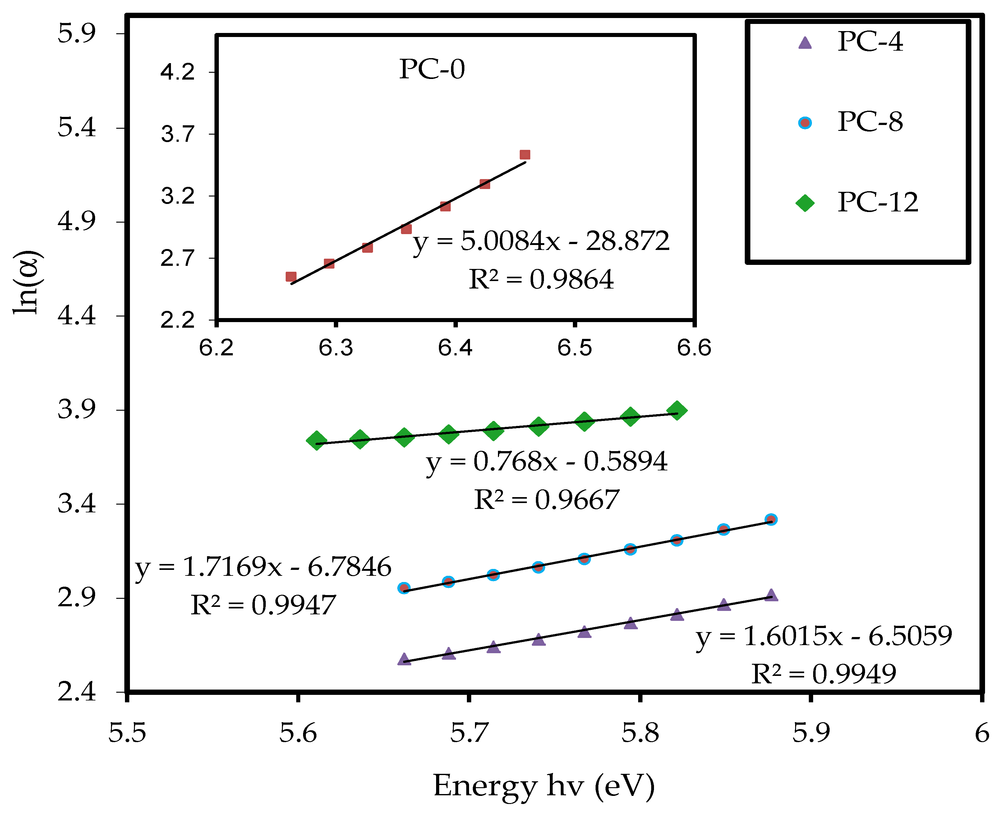
Table 2 reveals an overview of the band tail values of both PVA and PVA-loaded samples. The band tail values were determined from the inverse of the slopes associated with the lines given in
Figure 6. It has been emphasized that the
values increase as the PbS NPs amount is increased. The consequence of increasing the values produces tail-to-tail transitions, and it is an indication of the newly constructed localized states with relatively high density [
8,
41].
3.2.3. Study of Optical Band Gap Energy and Dielectric Loss
As a common approach, UV-vis spectroscopy is applied to measure the
Eg of materials. The electrons will excite due to photon energy absorption, leading to absorption edge modification. Consequently, some deviations will occur in the BG, which facilitates the determination of optical band gap energies [
39].
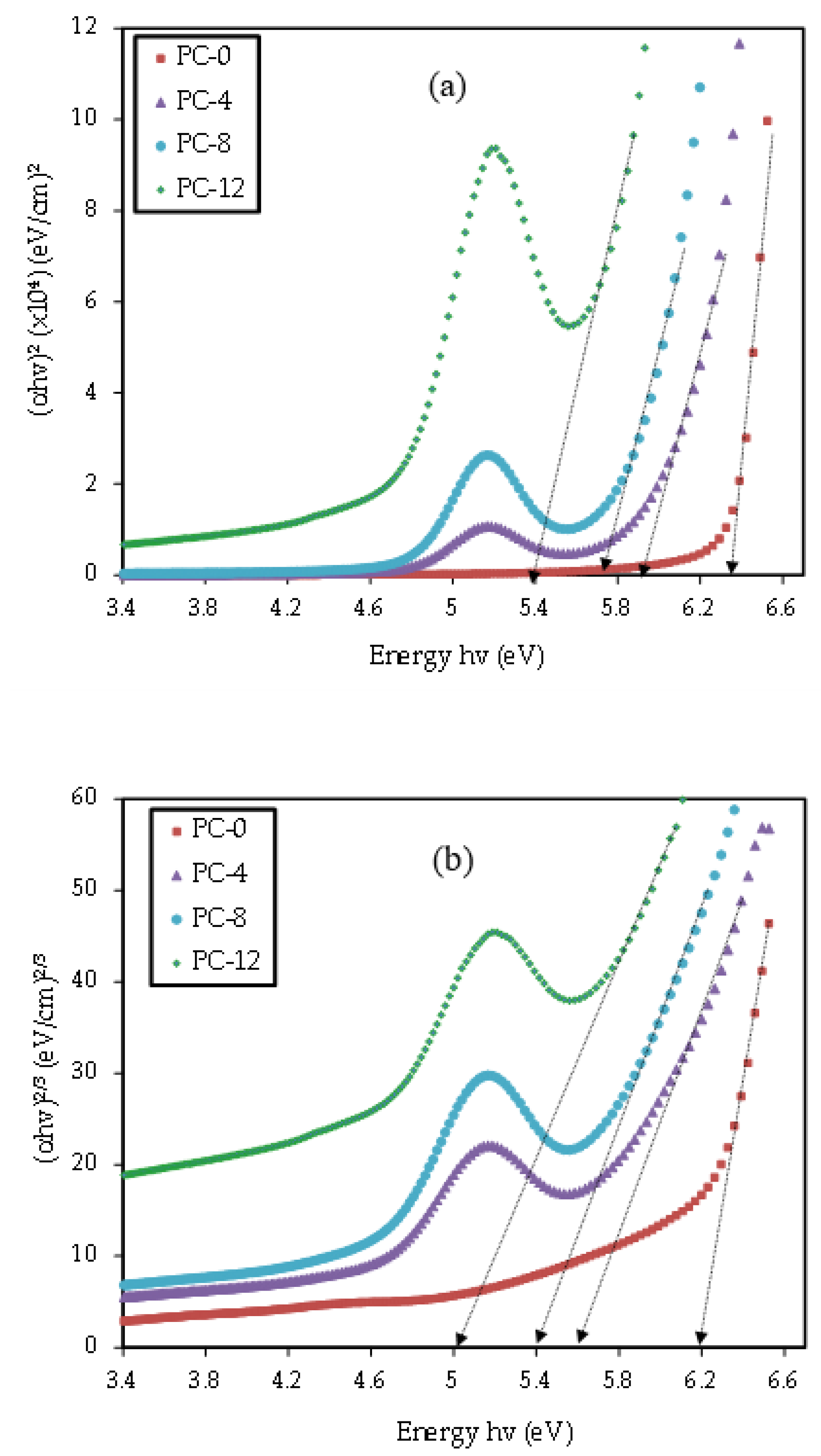
Figure 7a–d depict the plot of
with photon energy (
hv) and for all the systems. The values of
Eg of the samples also can be determined using the
ɛi approach. The optical
Eg is obtained from the Tauc’s equation using Equation (7) [
42,
43,
44].
where
B is a constant parameter related to the formation of new energy bands, and
represents the optical
Eg. The
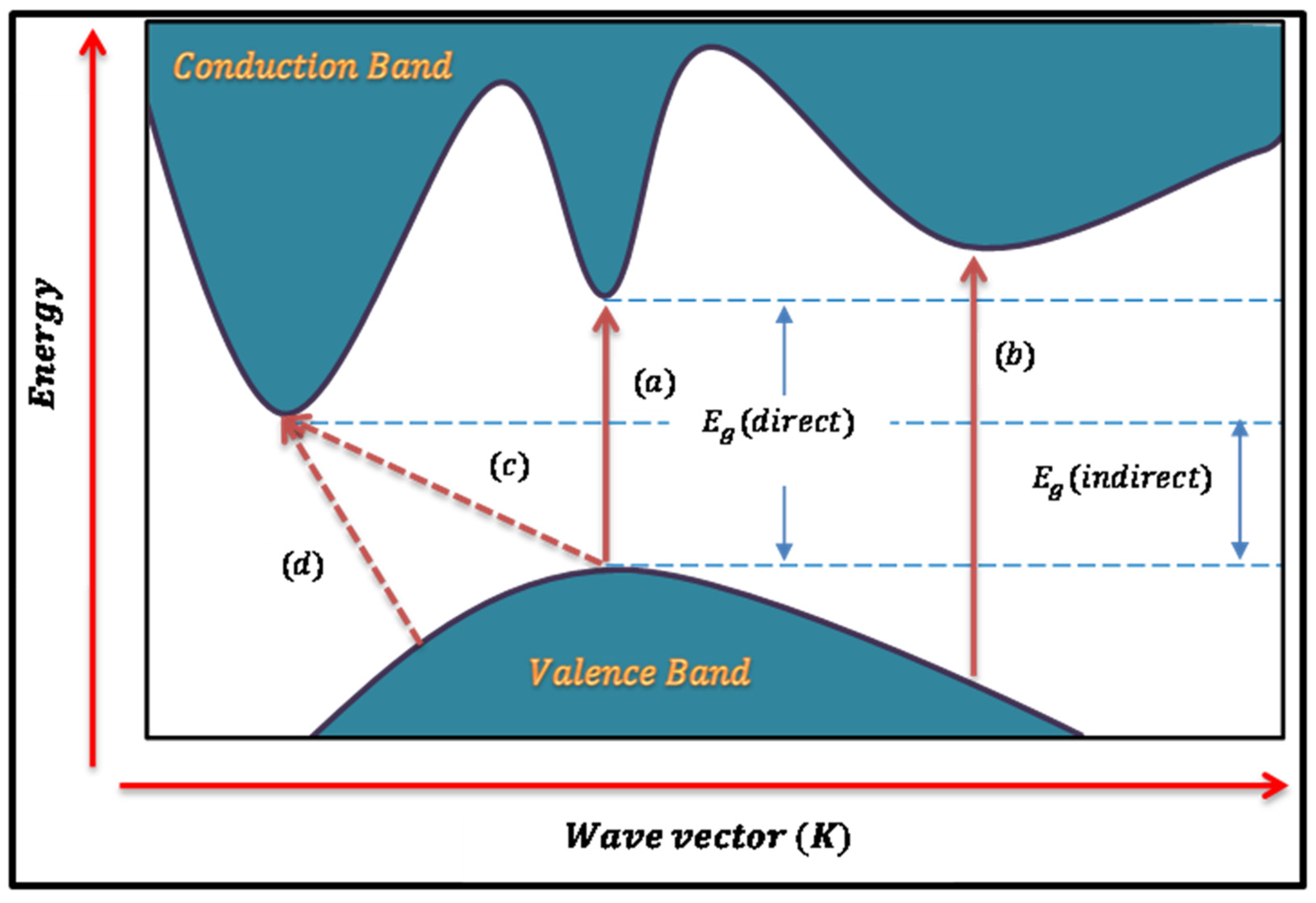
γ could take the values of 1/2 and 3/2, which indicate the electron transitions of direct allowed and forbidden, respectively. The
γ can also take the values of 2 and 3, which refer to indirect allowed and forbidden transitions, respectively.
Figure 8 shows the kinds of electronic transitions schematically. The intercept of the extrapolated linear components of the figure of
on the x-axis gives the direct optical
Eg of both the PVA and PVA composites [
45].
Table 3 tabulates the BG values corresponding to all possible transitions. The manipulation of newly formed levels between the valence band (V-B) and conduction band (C-B) of PVA is evidenced by the optical
Eg decrease from 6.3 eV for the PVA to 5.25 eV for PVA with 12 wt% of PbS NPs. This reduction also confirms that permanent defects occur at the band edge within the forbidden band. Moreover, it emphasizes that an intermediate energy level will be created in the forbidden gap [
46,
47]. This is also attributed to the influences of adding PbS NPs, which leads to creating extra electronic states in the PVA BG. Those states serve as intermediate locations for recombination and trapping, causing the optical band gap to modify. The polymer structure change causes an increase in the extent of disordering in the samples and a significant reduction in the
Eg [
48]. A report published in the literature stated the difficulty of measuring the direct and indirect kinds of amorphous materials [
49].
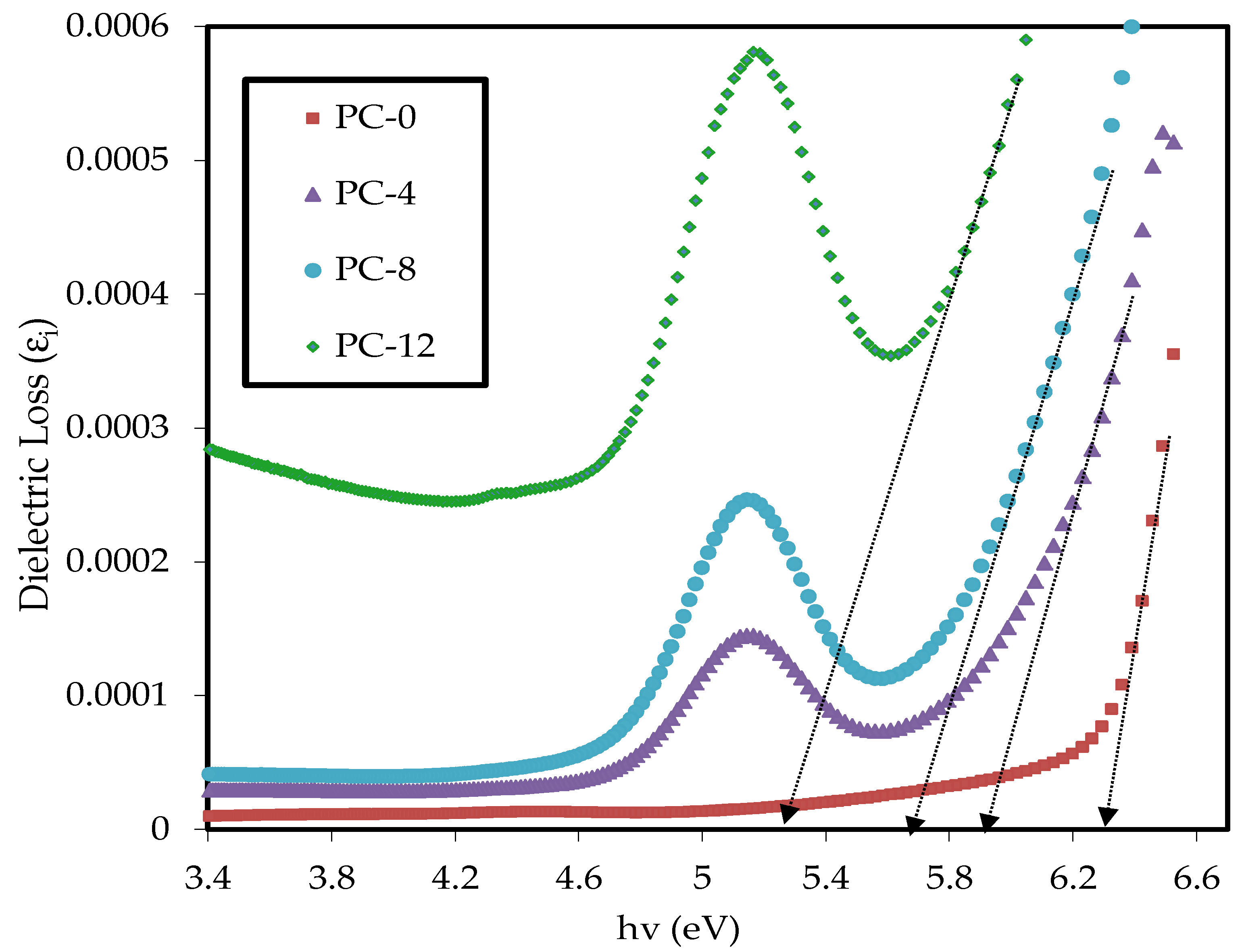
It is clear from
Table 3 that the estimated band gap values for composite samples for
γ = 3/2 (direct forbidden) are close enough to those obtained from the optical dielectric loss plot (
Figure 9), meaning that the crystalline structure is perturbed in the NCPs samples. Therefore, the direct forbidden (
γ = 3/2) results for NCPs samples are associated with the reduction of the crystalline order in PVA composite films. The
Eg achieved from Tauc’s equation (
Figure 7a–d) in comparison to the
Eg value obtained from the optical dielectric loss plot (
Figure 9) indicates that the nature of electronic transition in pure PVA is direct allowed (
γ = 1/2).
The current work shows the change in the BG of PVA loaded with PbS NPs and compares with those published for different polymers with several fillers, including ceramics, salts, metal complexes, and NPs.
Table 4 presents how the various filler additions in the previous works did not considerably change the
Eg of polymers.
Using the dielectric function from optical spectroscopy is vital to study the overall band structure of materials because of their strong correlation. The earlier study shows that the electron transition from occupied state to unoccupied state is primarily characterized by the imaginary component of the dielectric function (
) [
93]. However, there is a sophisticated quantum mechanical formulation which can precisely reflect the imaginary component of the dielectric constant [
94],
where the functions (Ψ
n′kσ and Ψ
nkσ) stand for the crystal wave functions from the final and initial states at the
k-point. The constant parameters,
e, Ω, and
m, are the electron charge, volume, and mass, respectively. The
represents the Fermi energy distribution. In the present study, the optical band gap of the samples was precisely and reliably assessed by applying the idea of optical dielectric loss. In recent years, it has been well established that the absorption edge could be derived from the mutual relationship between dielectric loss and photon energy with comparable outcomes to or almost the same as those obtained from the Tauc’s relationship [
28,
30,
42].
Based on the experimental results, a direct calculation of the dielectric function from optical spectroscopy is highly possible. Optical spectroscopy also eases access to crucial parameters such as absorbance, reflectance, refractive index, and extinction coefficient. Therefore, establishing a relationship between the measured parameters and the
and
is the aim of this work in the attempt to gain a comprehensive understanding of electronic structure within materials that respond to UV-vis radiation. Thus, the easy way of determining the complex dielectric constant from the achieved
n and
k is the implementation of the below correlation [
29]:
From
Figure 9, one can consider the actual band gap from the intersection of linear components with the x-axis. Nofal et al. [
40] have recently concluded that the principal absorption edge comes from the plot associated with dielectric loss versus
hυ. The study also emphasized that the absorption edge must be equivalent to or substantially near that calculated from Tauc’s theory [
40]. Moreover, it will be reasonable to effectively define the interband absorption mechanism from the electron transition between the solid bands. To be clearer, the optical transition onset over the BG is mainly determined by the absorption edge. As mentioned above, the electronic transition types can be measured by comparing the graphs from Tauc’s method (see
Figure 7a–d) to
Figure 9. From those figures, it was concluded that PVA’s electronic transition type is directly allowed, whereas PVA:PbS samples are directly forbidden. Eventually, from the previous findings, the band gap structure and the dielectric function can be analyzed [
63].
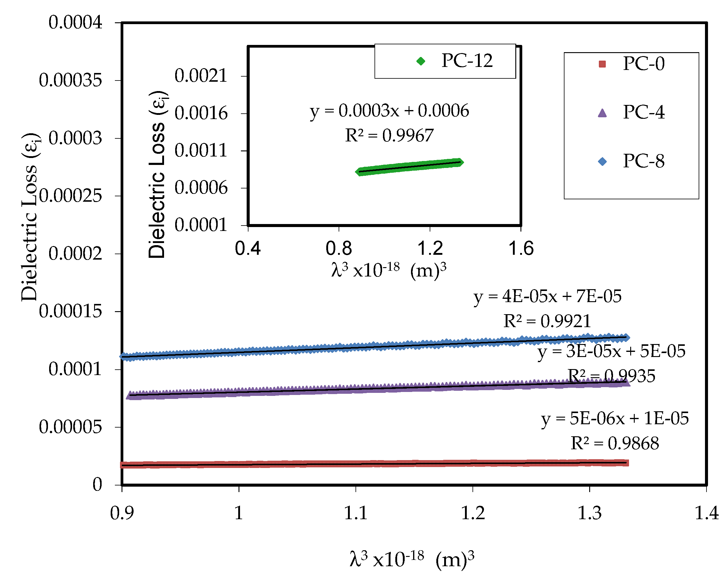
The long wavelength range and low frequency (
) are strongly correlated. This results in photons with low energy (
), making it impossible for them to move electrons from the V-B to the C-B. So, electrons lose energy by scattering. The optical characteristics of materials are described from the index of refraction and the dielectric constant. A clear relationship is seen in Equation (10), where
n and
K values can also be derived from
.
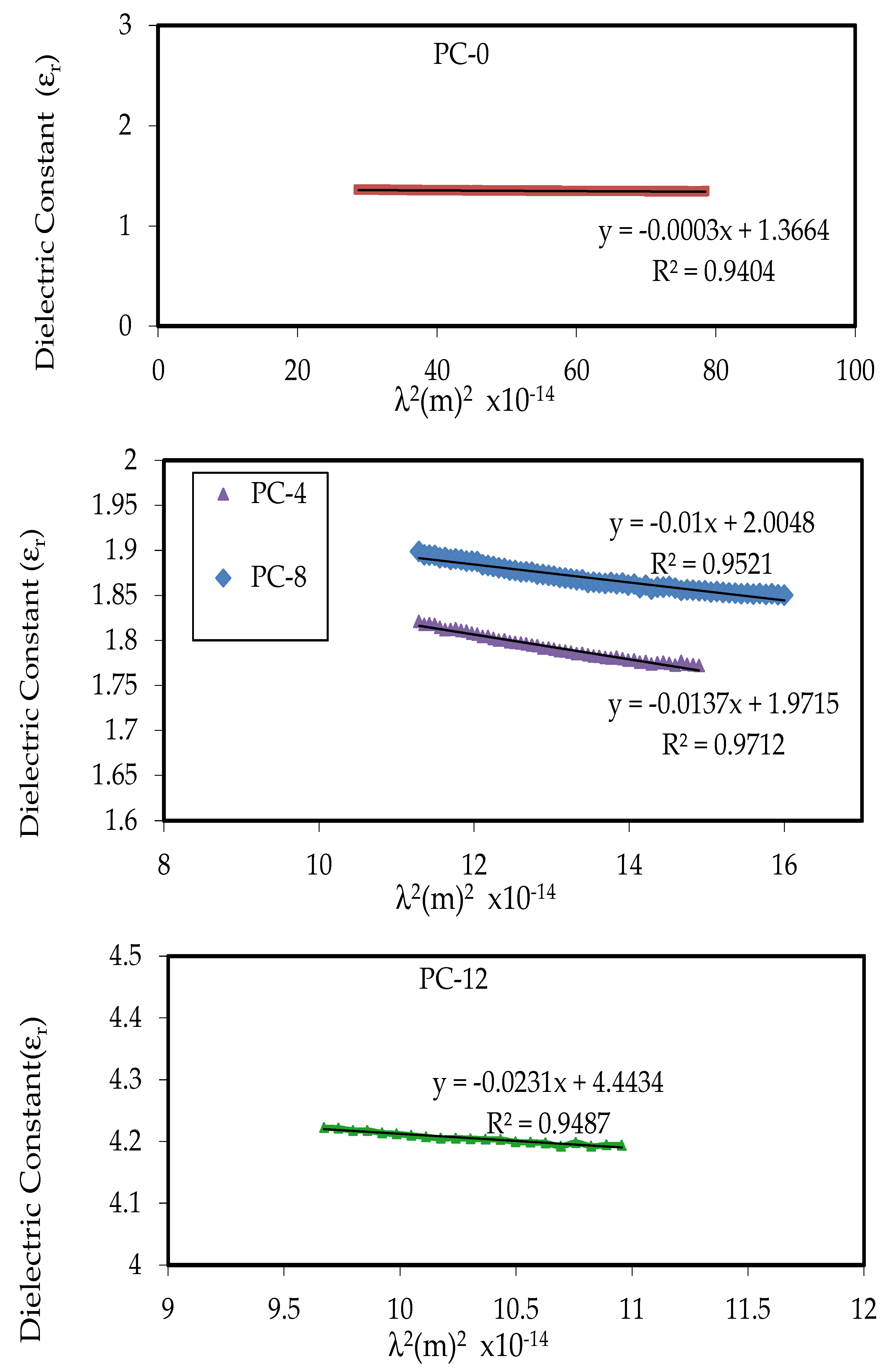
Figure 10 shows the essential interrelationship between the
and
λ for the samples. Based on the Spitzer–Fan model, the wavelength and refractive index relationship were used to obtain the dielectric response at high frequency (short wavelengths) [
95]:
where
,
and
arethe permittivity of vacuum, speed of light, and the amount of charge carrier per unit volume, respectively.
stands for the effective mass, which is 1.16
[
52].
Here, the dielectric constant in its complex form is equivalent to the complex refractive index square (
). Additionally, it indicates how much the material candecrease the speed of light [
48].
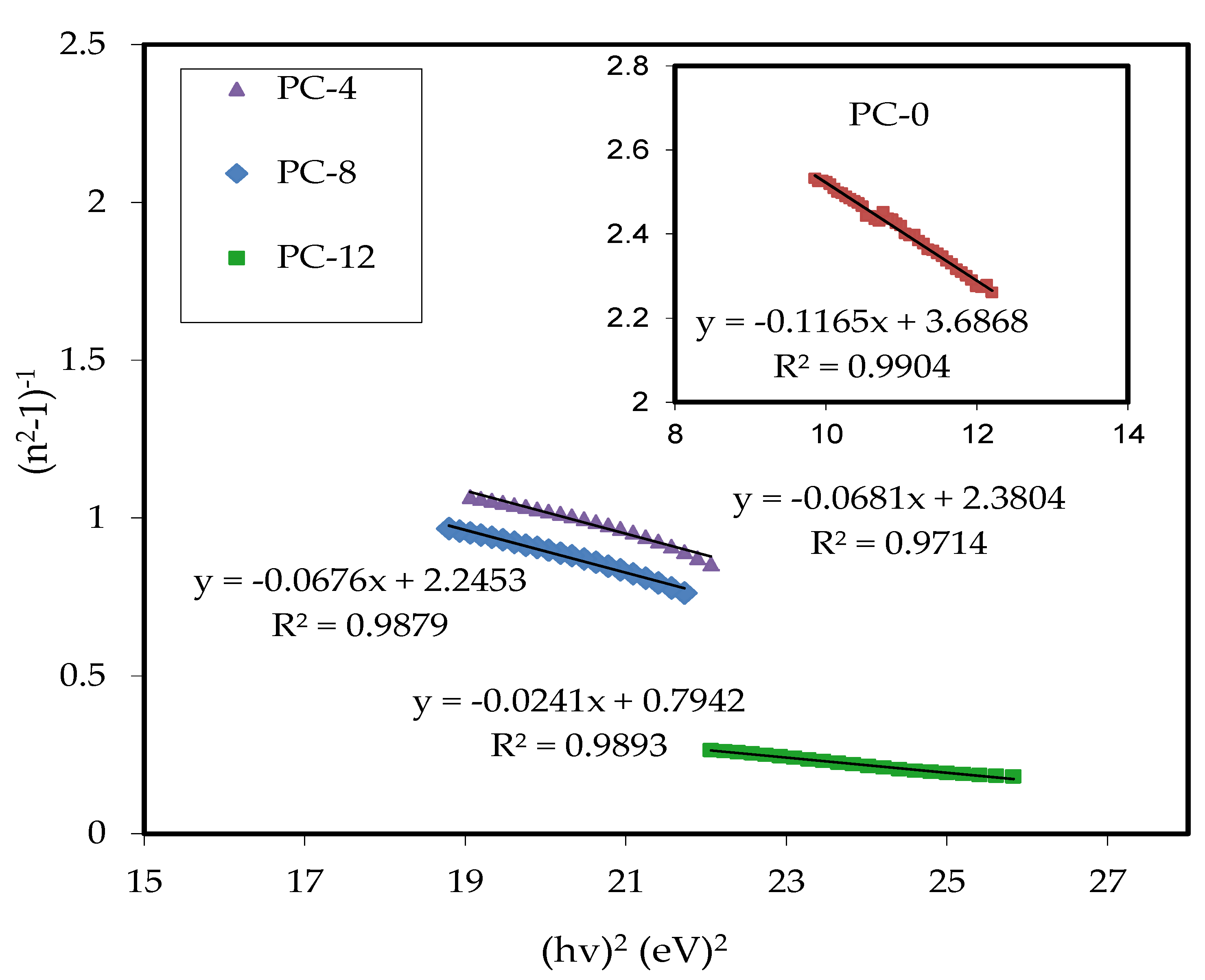
Figure 11shows the relationship between the
and
in the visible range. The slope value and intercept with the y-axis canbe applied to determine the
N/
m* and
values, respectively. The estimation of the values of
,
N/
m*, and
were obtained from Equation (11).
Table 5 shows that the magnitudes of charge carriers (
N/
m*) in pure PVA increased as the filler concentration increased from 3.65 × 10
55 to 281.02 × 10
55 m
3/Kg. Furthermore, the
increased from 1.37 to 4.44, indicating a rise in free charge carriers that effectively contributed to the polarization process [
52].
There is a connection between the CDF and the assessable optical values using simple equations, from which a roughcomputation of the optical properties of solids can be performed. The
and
and the density of newly induced localized states of electrons within the forbidden band gap have experienced behavior that is robustly in accordance with prior studies. Upon using (
N/
m*) values, the prediction of many other crucial parameters from the Drude free electron model is possible, such as relaxation time (
), plasma frequency (
), and electrical resistivity (
) [
40]:
Figure 12 shows the variation of
with respect to
for a pure PVA and the other films with various quantities of PbS NPs in the region where linear behavior is obtainable. The relaxation time (
) values would be derived from Equation (12) using the
N/
m* value and the slope of linear correlation of
versus
. Moreover, to calculate the optical mobility (
),
, and
of the electron, the following relationships can be applied [
40]:
Table 6 shows the values of
and
. It is worthmentioning that the
,
, and
of PVA are manipulated in a lower trend upon the addition of PbS NOF. This incorporation of the filler leads to a much faster relaxation response of the NCP molecules to the guided electromagnetic field than the unfilled one.
The low values of
,
and
are a result of slowing down the light beam through polymer material films with relatively larger refractive indices. The
of the electron increased from 1.06 × 10
29 to 81.5 × 10
29 Hz when the PbS NPs was added. A comparable outcome collected for NCPs and the effect of an intensive local electric field of induced NOF dipole moment has been reported. This enhances the material’s polarization whenever exposed to the external electromagnetic field. The calculation of optical parameters can also be carried out. The previous explanation indicates that there is more than one way to evaluate the
Eg such as using refractive index and the optical dielectric loss function. These factors are outstanding and decisive in choosing appropriate materials for optoelectronic applications [
40].
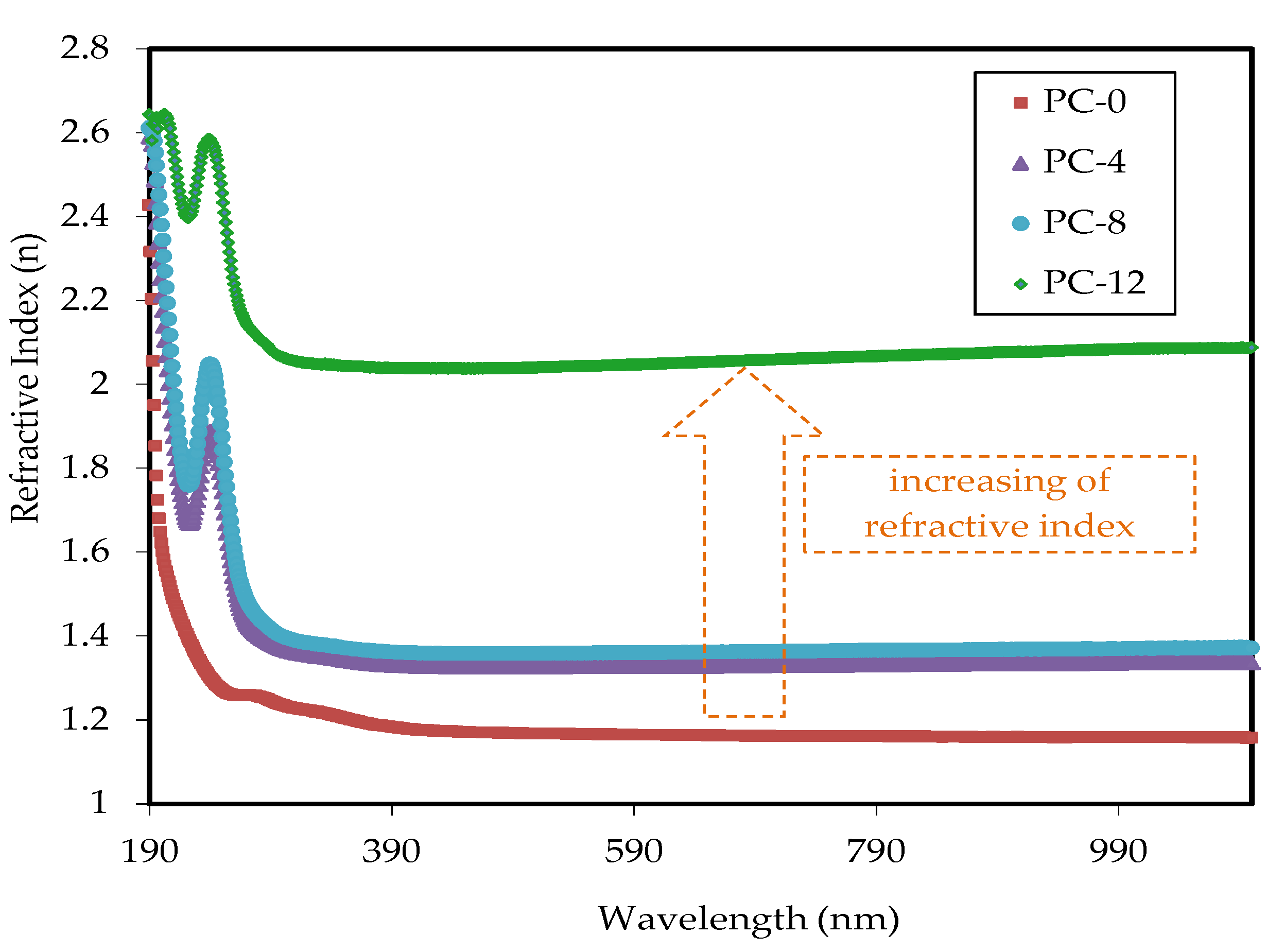
3.2.4. Refractive Index Study
Figure 13 shows the refractive index (
n) and wavelength correlation of PVA and loaded films. It is noticeable that the refractive index increases with the increase of PbS NPs. Recently, it has been observed that the demand for suitable optical materials with efficient
n has increased, particularly in a wide range of optical applications, such as ophthalmic lenses, optical adhesives, lenses, optoelectronics, filters, highly reflecting, and antireflecting coatings [
48,
84]. As seen in
Figure 13, the addition of PbS NPs increased the value of
n of the NCPs samples. Quantitatively, the
n values are increased from 1.27 to around 2.16. Lü et al. [
96] described how adding some semiconductor NPs of metal sulfide, such as PbS, which have a high refractive index, into a polymer matrix, fabricates NCPs with a high refractive index.
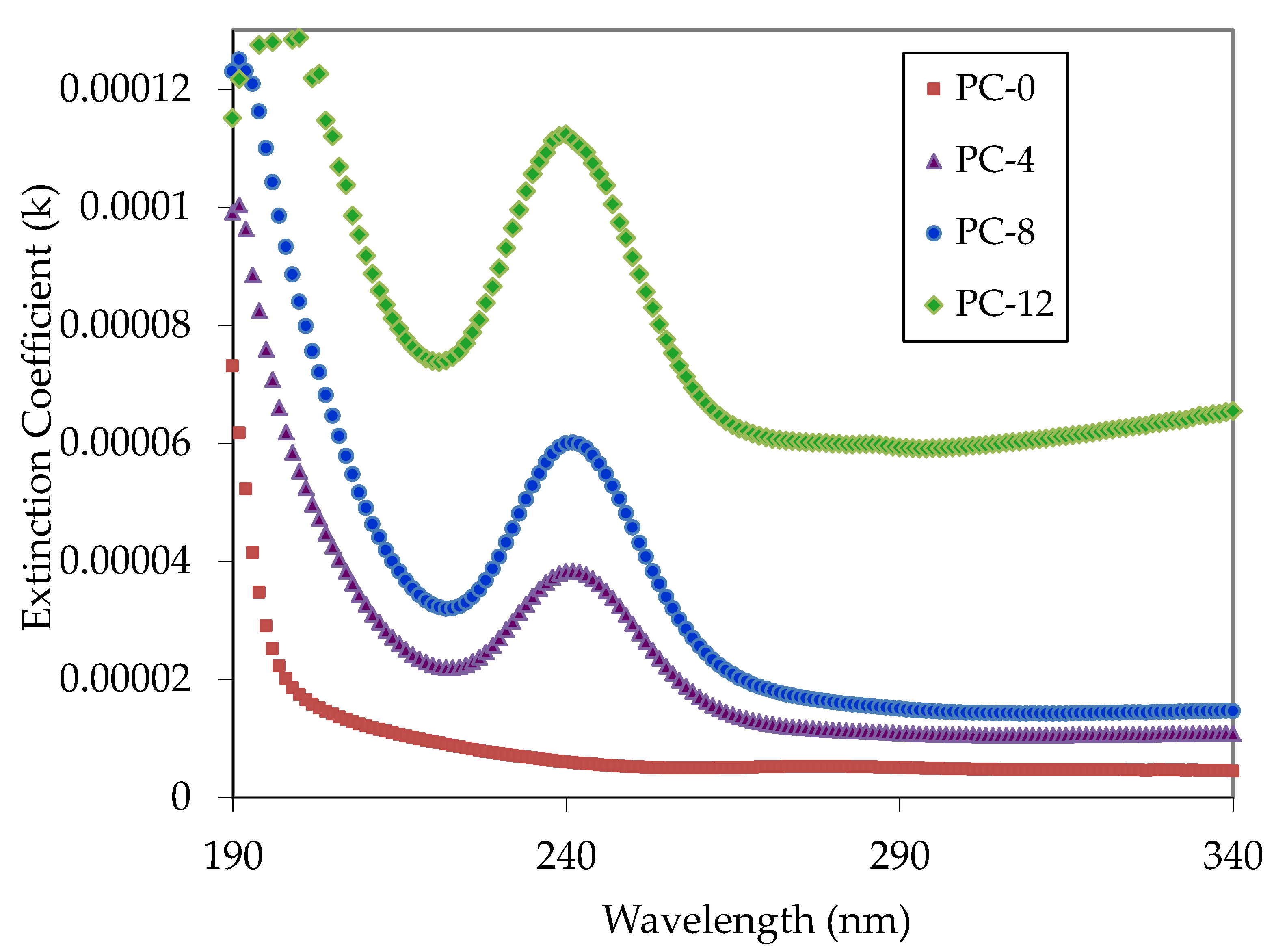
The extinction coefficient (
K) and wavelength relationship are shown in
Figure 14. By applying Kramers–Kronig relationships, the
n values are obtained from
R and
K [
52]:
where
.
The
k has a high value for the loaded samples at longer wavelengths. The
k determines the amount of light loss because of absorption and scattering per unit distance of the guiding medium. The magnitude of (
k) shows the degree of transparency of the films at the long wavelengths [
48].
On the other hand, at short wavelengths the
k obtains the maximum value immediately because the absorption behavior predominates.
Figure 14 shows that k increases when the PbS NPs quantity in PVA films increases. When the material under study is subjected to electromagnetic radiation, the composite films dissipate higher energy than those made that of pure PVA, according to the higher
k value [
73].

 ,
, 


