
The Impact of Topological States on the Thermoelectric Performance of p- and n-Type Sb2Te3/Bi2Se3-Multiwalled Carbon Nanotubes Heterostructured Networks

Abstract
:1. Introduction
2. Materials and Methods
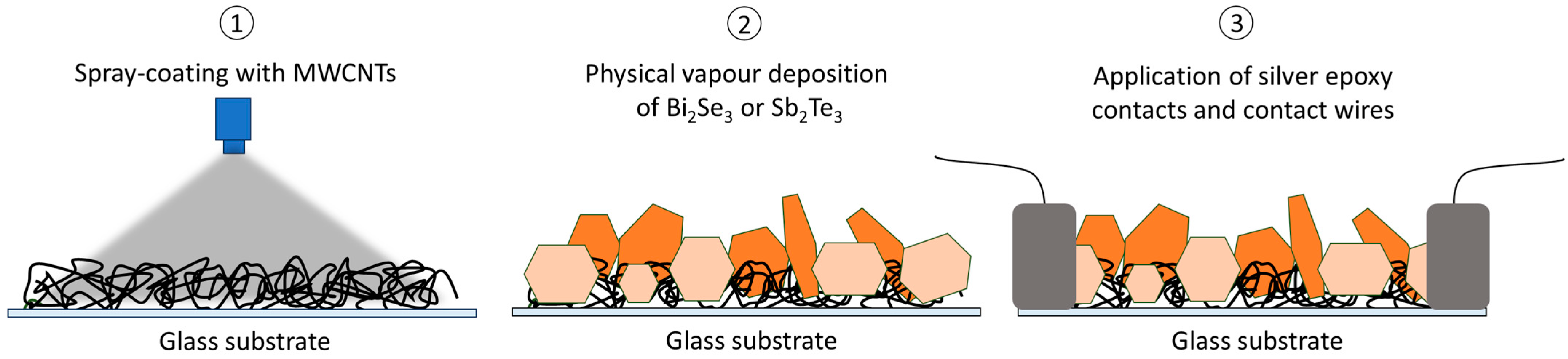
2.1. Synthesis of MWCNTs
2.2. Synthesis of Sb2Te3/Bi2Se3-MWCNT Heterostructures
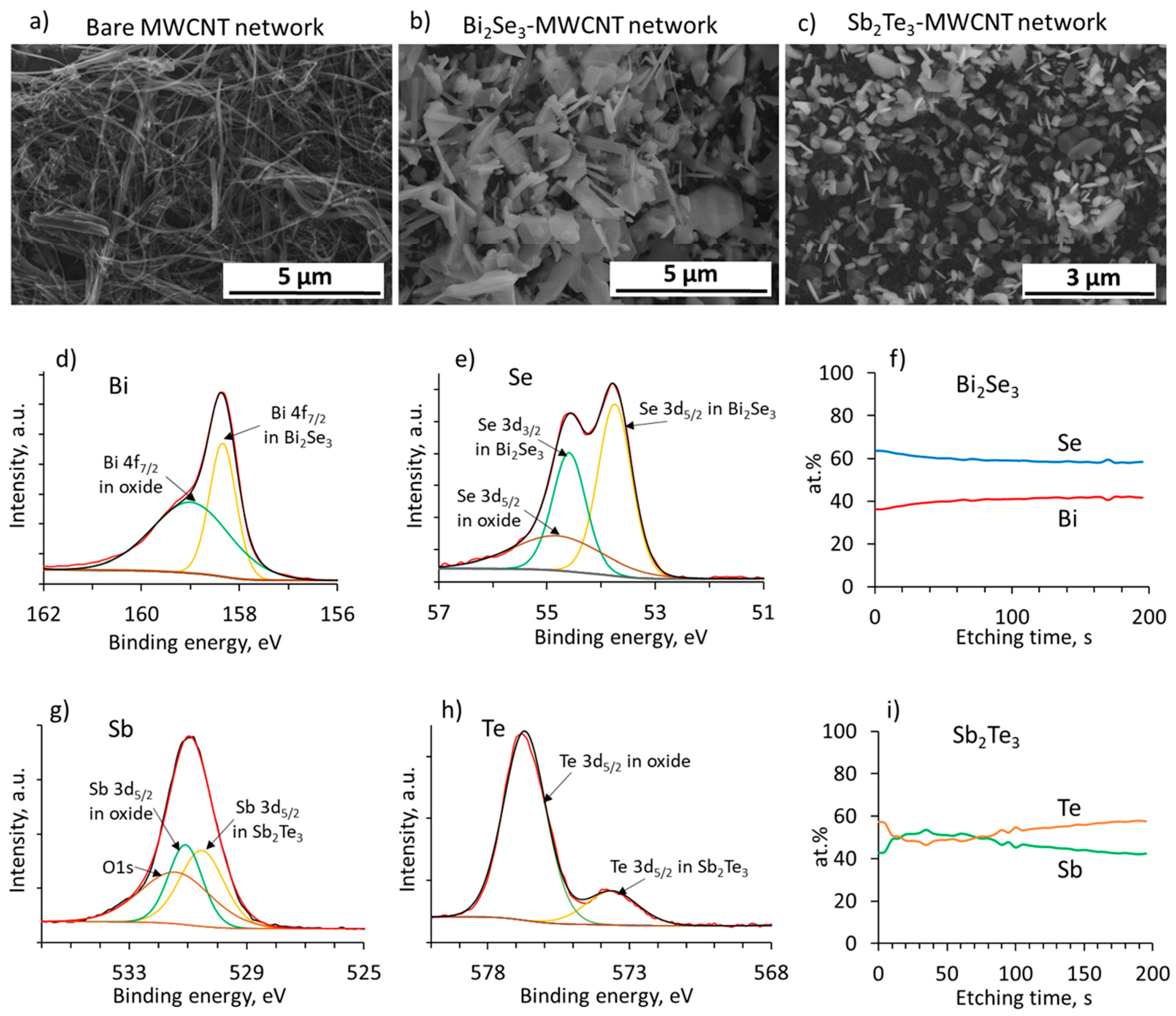
2.3. The Morphology and Chemical Composition of the Samples
2.4. Room-Temperature Seebeck Coefficient Measurements
2.5. Magnetoresistance Measurements in the Temperature Range 2–300 K
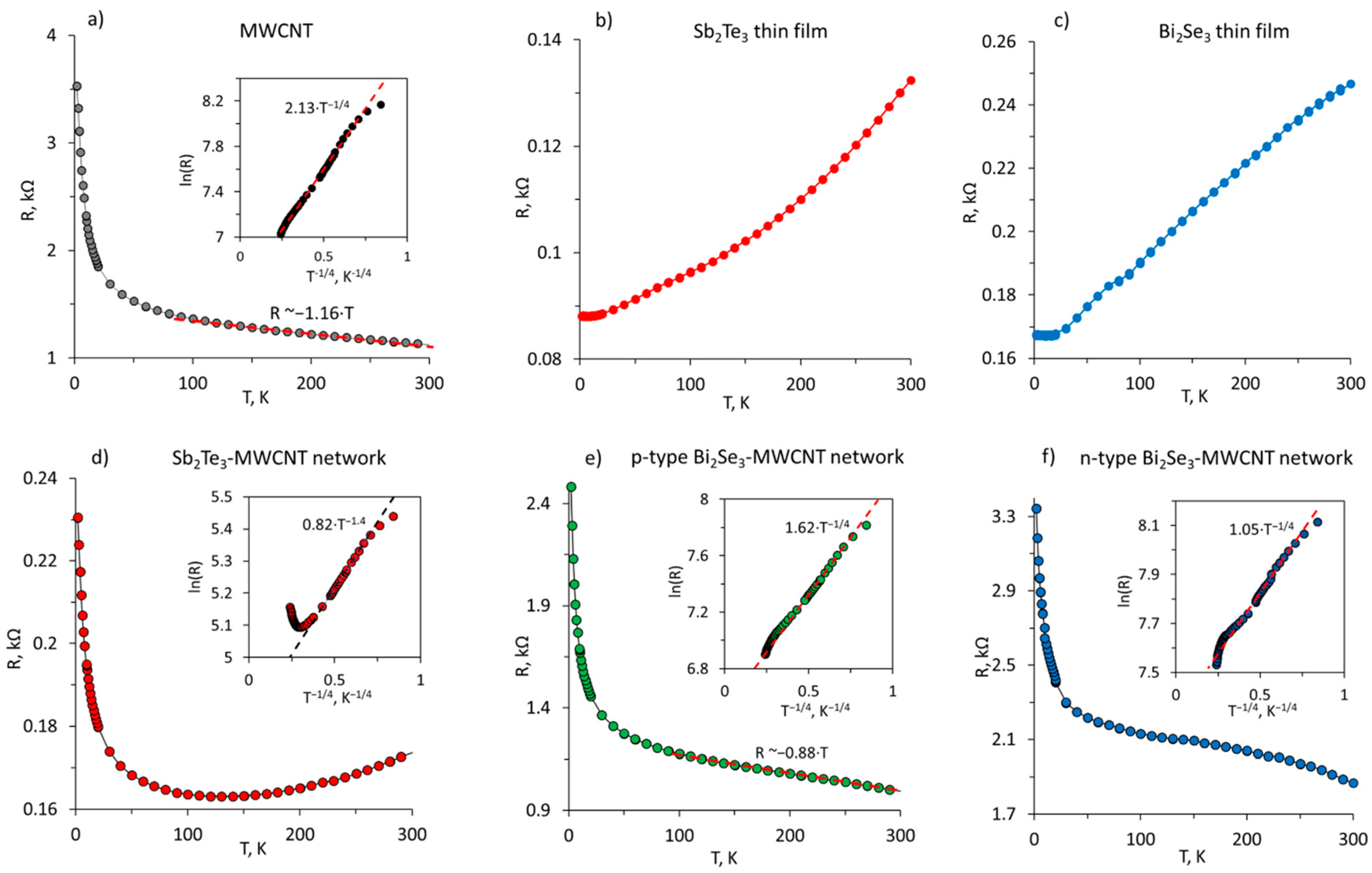
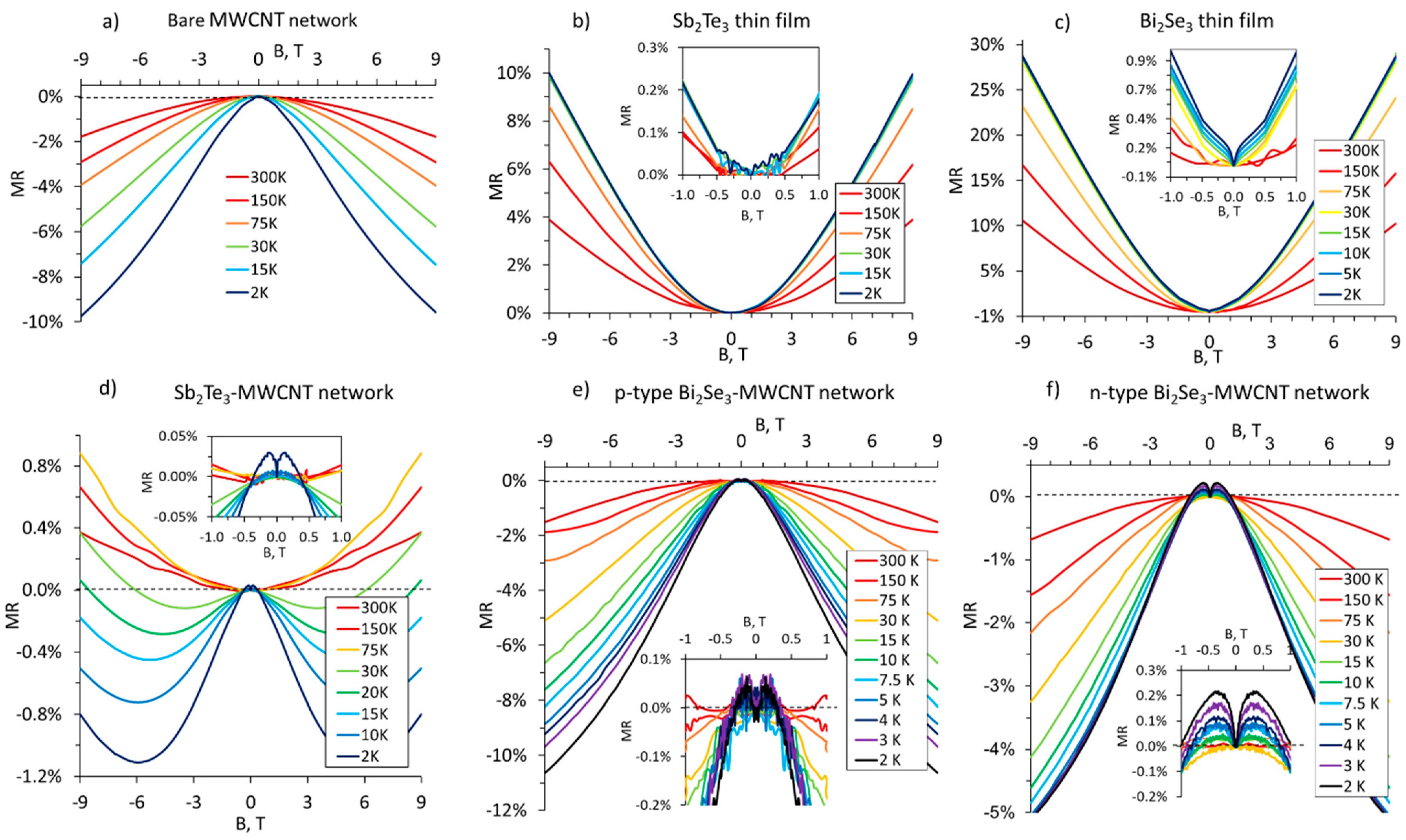
3. Results and Discussion
4. Conclusions
Author Contributions
Funding
Institutional Review Board Statement
Informed Consent Statement
Data Availability Statement
Acknowledgments
Conflicts of Interest
References
- He, R.; Schierning, G.; Nielsch, K. Thermoelectric Devices: A Review of Devices, Architectures, and Contact Optimization. Adv. Mater. Technol. 2018, 3, 1700256. [Google Scholar] [CrossRef]
- Yadav, A.; Deshmukh, P.C.; Roberts, K.; Jisrawi, N.M.; Valluri, S.R. An analytic study of the Wiedemann–Franz law and the thermoelectric figure of merit. J. Phys. Commun. 2019, 3, 105001. [Google Scholar] [CrossRef]
- Fang, L.; Jia, Y.; Miller, D.J.; Latimer, M.L.; Xiao, Z.L.; Welp, U.; Crabtree, G.W.; Kwok, W.K. Catalyst-free growth of millimeter-long topological insulator Bi2Se3 nanoribbons and the observation of the π-berry phase. Nano Lett. 2012, 12, 6164–6169. [Google Scholar] [CrossRef]
- Kim, D.; Syers, P.; Butch, N.P.; Paglione, J.; Fuhrer, M.S. Ambipolar surface state thermoelectric power of topological insulator Bi2Se3. Nano Lett. 2014, 14, 1701–1706. [Google Scholar] [CrossRef] [PubMed]
- Kumar, A.; Cecchini, R.; Locatelli, L.; Wiemer, C.; Martella, C.; Nasi, L.; Lazzarini, L.; Mantovan, R.; Longo, M. Large-Area MOVPE Growth of Topological Insulator Bi2Te3 Epitaxial Layers on i-Si(111). Cryst. Growth Des. 2021, 21, 4023–4029. [Google Scholar] [CrossRef]
- Sung, J.H.; Heo, H.; Hwang, I.; Lim, M.; Lee, D.; Kang, K.; Choi, H.C.; Park, J.H.; Jhi, S.H.; Jo, M.H. Atomic layer-by-layer thermoelectric conversion in topological insulator bismuth/antimony tellurides. Nano Lett. 2014, 14, 4030–4035. [Google Scholar] [CrossRef]
- Chudzinski, P. Contribution of 1D topological states to the extraordinary thermoelectric properties of Bi2Te3. Proc. R. Soc. A Math. Phys. Eng. Sci. 2020, 476, 20200088. [Google Scholar] [CrossRef]
- Ghaemi, P.; Mong, R.S.K.; Moore, J.E. In-plane transport and enhanced thermoelectric performance in thin films of the topological insulators Bi2Te3 and Bi2Se3. Phys. Rev. Lett. 2010, 105, 166603. [Google Scholar] [CrossRef]
- Tahir, M.; Manchon, A.; Schwingenschlögl, U. Enhanced thermoelectric power in ultrathin topological insulators with magnetic doping. J. Appl. Phys. 2014, 116, 093708. [Google Scholar] [CrossRef]
- Guo, M.; Wang, Z.; Xu, Y.; Huang, H.; Zang, Y.; Liu, C.; Duan, W.; Gan, Z.; Zhang, S.C.; He, K.; et al. Tuning thermoelectricity in a Bi2Se3 topological insulator via varied film thickness. New J. Phys. 2016, 18, 015008. [Google Scholar] [CrossRef]
- Andzane, J.; Felsharuk, A.; Sarakovskis, A.; Malinovskis, U.; Kauranens, E.; Bechelany, M.; Niherysh, K.A.; Komissarov, I.V.; Erts, D. Thickness-dependent properties of ultrathin bismuth and antimony chalcogenide films formed by physical vapor deposition and their application in thermoelectric generators. Mater. Today Energy 2021, 19, 100587. [Google Scholar] [CrossRef]
- Jin, Q.; Jiang, S.; Zhao, Y.; Wang, D.; Qiu, J.; Tang, D.M.; Tan, J.; Sun, D.M.; Hou, P.X.; Chen, X.Q.; et al. Flexible layer-structured Bi2Te3 thermoelectric on a carbon nanotube scaffold. Nat. Mater. 2019, 18, 62–68. [Google Scholar] [CrossRef] [PubMed]
- Zhao, Y.; Li, Y.; Qiao, J.; Jiang, S.; Mao, P.; Qiu, J.; Kang, S.; Tan, J.; Tai, K.; Liu, C. Decoupling phonon and carrier scattering at carbon nanotube/Bi2Te3 interfaces for improved thermoelectric performance. Carbon N. Y. 2020, 170, 191–198. [Google Scholar] [CrossRef]
- Li, Y.; Zhao, Y.; Qiao, J.; Jiang, S.; Qiu, J.; Tan, J.; Zhang, L.; Gai, Z.; Tai, K.; Liu, C. A Flexible and Infrared-Transparent Bi2Te3-Carbon Nanotube Thermoelectric Hybrid for both Active and Passive Cooling. ACS Appl. Electron. Mater. 2020, 2, 3008–3016. [Google Scholar] [CrossRef]
- Tseng, S.C.; Wang, C.A.; Chu, H.S.; Tsai, H.Y. Thermoelectric properties of a vertically aligned carbon nanotube array with embedded bismuth telluride. J. Mater. Sci. 2022, 57, 19396–19404. [Google Scholar] [CrossRef]
- Buks, K.; Andzane, J.; Smits, K.; Zicans, J.; Bitenieks, J.; Zarins, A.; Erts, D. Growth mechanisms and related thermoelectric properties of innovative hybrid networks fabricated by direct deposition of Bi2Se3 and Sb2Te3 on multiwalled carbon nanotubes. Mater. Today Energy 2020, 18, 100526. [Google Scholar] [CrossRef]
- Kumanek, B.; Janas, D. Thermal conductivity of carbon nanotube networks: A review. J. Mater. Sci. 2019, 54, 7397–7427. [Google Scholar] [CrossRef]
- Kulbachinskii, V.A.; Kytin, V.G.; Kudryashov, A.A.; Tarasov, P.M. Thermoelectric properties of Bi2Te3, Sb2Te3 and Bi2Se3 single crystals with magnetic impurities. J. Solid State Chem. 2012, 193, 47–52. [Google Scholar] [CrossRef]
- Osterhage, H.; Gooth, J.; Hamdou, B.; Gwozdz, P.; Zierold, R.; Nielsch, K. Thermoelectric properties of topological insulator Bi2Te3, Sb2Te3, and Bi2Se3 thin film quantum wells. Appl. Phys. Lett. 2014, 105, 123117. [Google Scholar] [CrossRef]
- Andzane, J.; Buks, K.; Bitenieks, J.; Bugovecka, L.; Kons, A.; Merijs-meri, R.; Svirksts, J.; Zicans, J.; Erts, D. p-Type PVA/MWCNT-Sb2Te3 Composites for Application in Different Types of Flexible Thermoelectric Generators in Combination with n-Type PVA/MWCNT-Bi2Se3 Composites. Polymers 2022, 14, 5130. [Google Scholar] [CrossRef]
- Buks, K.; Andzane, J.; Bugovecka, L.; Katkov, M.V.; Smits, K.; Starkova, O.; Katkevics, J.; Bērziņš, A.; Brauna, L.; Voikiva, V.; et al. Highly Efficient Flexible n-Type Thermoelectric Films Formed by Encapsulation of Bi2Se3-MWCNT Hybrid Networks in Polyvinyl Alcohol. Adv. Mater. Interfaces 2022, 9, 2200318. [Google Scholar] [CrossRef]
- Bugovecka, L.; Buks, K.; Andzane, J.; Miezubrale, A.D.; Bitenieks, J.; Zicans, J.; Erts, D. Positive and Negative Changes in the Electrical Conductance Related to Hybrid Filler Distribution Gradient in Composite Flexible Thermoelectric Films Subjected to Bending. Nanomaterials 2023, 13, 1212. [Google Scholar] [CrossRef] [PubMed]
- Gracia-Abad, R.; Sangiao, S.; Bigi, C.; Chaluvadi, S.K.; Orgiani, P.; De Teresa, J.M. Omnipresence of weak antilocalization (WAL) in Bi2Se3 thin films: A review on its origin. Nanomaterials 2021, 11, 1077. [Google Scholar] [CrossRef] [PubMed]
- Kuzanyan, A.A.; Harutyunyan, S.R. Weak Localization and Weak Anti-Localization in Ultra Thin Sb2Te3 Nanoplates. J. Contemp. Phys. 2021, 56, 359–365. [Google Scholar] [CrossRef]
- Ding, D.; Dai, X.; Wang, C.; Diao, D. Temperature dependent crossover between positive and negative magnetoresistance in graphene nanocrystallines embedded carbon film. Carbon N. Y. 2020, 163, 19–25. [Google Scholar] [CrossRef]
- Garg, R.; Gopalan, D.P.; De La Barrera, S.C.; Hafiz, H.; Nuhfer, N.T.; Viswanathan, V.; Hunt, B.M.; Cohen-Karni, T. Electron Transport in Multidimensional Fuzzy Graphene Nanostructures. Nano Lett. 2019, 19, 5335–5339. [Google Scholar] [CrossRef]
- Bao, L.; He, L.; Meyer, N.; Kou, X.; Zhang, P.; Chen, Z.G.; Fedorov, A.V.; Zou, J.; Riedemann, T.M.; Lograsso, T.A.; et al. Weak anti-localization and quantum oscillations of surface states in topological insulator Bi2Se2Te. Sci. Rep. 2012, 2, 726. [Google Scholar] [CrossRef]
- Salvato, M.; Lucci, M.; Ottaviani, I.; Cirillo, M.; Orlanducci, S.; Toschi, F.; Terranova, M.L. Weak localization and dimensional crossover in carbon nanotube systems. Eur. Phys. J. B 2012, 85, 2–6. [Google Scholar] [CrossRef]
- Takane, Y. Weak localization in multiwall carbon nanotubes in a perpendicular magnetic field. J. Phys. Soc. Japan 2006, 75, 044701. [Google Scholar] [CrossRef]
- Ovsiienko, I.; Len, T.; Mirzoiev, I.; Beliayev, E.; Gnida, D.; Matzui, L.; Heraskevych, V. Low-temperature magnetoresistance of functionalized multiwall carbon nanotubes. Fiz. Nizk. Temp. 2023, 49, 17–33. [Google Scholar] [CrossRef]
- Wolf, S.A.; Awschalom, D.D.; Buhrman, R.A.; Daughton, J.M.; Von Molnár, S.; Roukes, M.L.; Chtchelkanova, A.Y.; Treger, D.M. Spintronics: A spin-based electronics vision for the future. Science 2001, 294, 1488–1495. [Google Scholar] [CrossRef] [PubMed]
- Pulizzi, F. Spintronics. Nat. Mater. 2012, 11, 367. [Google Scholar] [CrossRef] [PubMed]
- Ahn, E.C. 2D materials for spintronic devices. Npj 2D Mater. Appl. 2020, 4, 17. [Google Scholar] [CrossRef]
- Zeng, J.; Chen, K.Q. Magnetic configuration dependence of magnetoresistance in a Fe-porphyrin-like carbon nanotube spintronic device. Appl. Phys. Lett. 2014, 104, 033104. [Google Scholar] [CrossRef]
- Andzane, J.; Katkov, M.V.; Buks, K.; Sarakovskis, A.; Smits, K.; Erts, D. Synthesis, magnetoresistance and thermoelectical properties of environmentally-stable n-type nitrogen-doped multiwalled carbon nanotubes. Carbon Trends 2023, 13, 100302. [Google Scholar] [CrossRef]
- Andzane, J.; Buks, K.; Strakova, M.N.; Zubkins, M.; Bechelany, M.; Marnauza, M.; Baitimirova, M.; Erts, D. Structure and Doping Determined Thermoelectric Properties of Bi2Se3 Thin Films Deposited by Vapour-Solid Technique. IEEE Trans. Nanotechnol. 2019, 18, 948–954. [Google Scholar] [CrossRef]
- Andzane, J.; Britala, L.; Kauranens, E.; Neciporenko, A.; Baitimirova, M.; Lara-Avila, S.; Kubatkin, S.; Bechelany, M.; Erts, D. Effect of graphene substrate type on formation of Bi2Se3 nanoplates. Sci. Rep. 2019, 9, 4791. [Google Scholar] [CrossRef] [PubMed]
- Boschker, J.E.; Galves, L.A.; Flissikowski, T.; Lopes, J.M.J.; Riechert, H.; Calarco, R. Coincident-site lattice matching during van der Waals epitaxy. Sci. Rep. 2015, 5, 18079. [Google Scholar] [CrossRef]
- Schaumann, J.; Loor, M.; Ünal, D.; Mudring, A.; Heimann, S.; Hagemann, U.; Schulz, S.; Maculewicz, F.; Schierning, G. Improving the zT value of thermoelectrics by nanostructuring: Tuning the nanoparticle morphology of Sb2Te3 by using ionic liquids. Dalt. Trans. 2017, 46, 656–668. [Google Scholar] [CrossRef]
- Idriss, H. On the wrong assignment of the XPS O1s signal at 531–532 eV attributed to oxygen vacancies in photo- and electro-catalysts for water splitting and other materials applications. Surf. Sci. 2021, 712, 2–7. [Google Scholar] [CrossRef]
- Meng, C.; Liu, C.; Fan, S. A promising approach to enhanced thermoelectric properties using carbon nanotube networks. Adv. Mater. 2010, 22, 535–539. [Google Scholar] [CrossRef] [PubMed]
- Andzane, J.; Spalva, E.; Katkevics, J.; Bugovecka, L.; Kons, A.; Buks, K.; Erts, D. Thermoelectrical properties of bare and PDMS-encapsulated MWCNT-Sb2Te3 hybrid networks and their application in flexible heat-to-power conversion devices. ACS Appl. Energy Mater. 2023, 6, 10807–10816. [Google Scholar] [CrossRef]
- Harutyunyan, S.R. Thickness-dependent magnetoresistance of Sb2Te3 nanoflakes and weak antilocalization effect. J. Contemp. Phys. 2015, 50, 282–287. [Google Scholar] [CrossRef]
- Jash, A.; Kumar, A.; Ghosh, S.; Bharathi, A.; Banerjee, S.S. Imaging current distribution in a topological insulator Bi2Se3 in the presence of competing surface and bulk contributions to conductivity. Sci. Rep. 2021, 11, 7445. [Google Scholar] [CrossRef] [PubMed]
- Kunakova, G.; Galletti, L.; Charpentier, S.; Andzane, J.; Erts, D.; Léonard, F.; Spataru, C.D.; Bauch, T.; Lombardi, F. Bulk-free topological insulator Bi2Se3 nanoribbons with magnetotransport signatures of Dirac surface states. Nanoscale 2018, 10, 19595–19602. [Google Scholar] [CrossRef] [PubMed]
- Xue, J.; Huang, S.; Wang, J.Y.; Xu, H.Q. Mott variable-range hopping transport in a MoS2 nanoflake. RSC Adv. 2019, 9, 17885–17890. [Google Scholar] [CrossRef]
- Yu, D.; Wang, C.; Wehrenberg, B.L.; Guyot-Sionnest, P. Variable range hopping conduction in semiconductor nanocrystal solids. Phys. Rev. Lett. 2004, 92, 216802. [Google Scholar] [CrossRef]
- Gupta, K.; Mukherjee, P.S.; Meikap, A.K.; Jana, P.C. Effect of samarium nanoparticles on the electrical transport properties of polyaniline. Adv. Nat. Sci. Nanosci. Nanotechnol. 2014, 5, 025003. [Google Scholar] [CrossRef]
- Lähderanta, E.; Hajdeu-Chicarosh, E.; Guc, M.; Shakhov, M.A.; Zakharchuk, I.; Bodnar, I.V.; Arushanov, E.; Lisunov, K.G. Magnetotransport and conductivity mechanisms in Cu2ZnSnxGe1−xS4 single crystals. Sci. Rep. 2018, 8, 17507. [Google Scholar] [CrossRef]
- Spataru, C.D.; Léonard, F. Fermi-level pinning, charge transfer, and relaxation of spin-momentum locking at metal contacts to topological insulators. Phys. Rev. B Condens. Matter Mater. Phys. 2014, 90, 085115. [Google Scholar] [CrossRef]
- Kumar, S.; Faraz, M.; Khare, N. Enhanced thermoelectric properties of Sb2Te3-graphene nanocomposite. Mater. Res. Express 2019, 6, 085079. [Google Scholar] [CrossRef]
- Tanty, N.; Patra, A.; Maity, K.P.; Prasad, V. Tuning magnetoresistance and electrical resistivity by enhancing localization length in polyaniline and carbon nanotube composites. Bull. Mater. Sci. 2019, 42, 198. [Google Scholar] [CrossRef]
- Ovsiienko, I.V.; Len, T.A.; Mirzoiev, I.G.; Beliayev, E.Y.; Gnida, D.; Matzui, L.Y.; Heraskevych, V.M. Low-temperature magnetoresistance of multi-walled carbon nanotubes with perfect structure. Low Temp. Phys. 2022, 48, 89–98. [Google Scholar] [CrossRef]
- Li, Q.; Li, Y.; Zhang, X.; Chikkannanavar, S.B.; Zhao, Y.; Dangelewicz, A.M.; Zheng, L.; Doorn, S.K.; Jia, Q.; Peterson, D.E.; et al. Structure-dependent electrical properties of carbon nanotube fibers. Adv. Mater. 2007, 19, 3358–3363. [Google Scholar] [CrossRef]
- Antonova, I.V.; Nebogatikova, N.A.; Stepina, N.P.; Volodin, V.A.; Kirienko, V.V.; Rybin, M.G.; Obrazstova, E.D.; Golyashov, V.A.; Kokh, K.A.; Tereshchenko, O.E. Growth of Bi2Se3/graphene heterostructures with the room temperature high carrier mobility. J. Mater. Sci. 2021, 56, 9330–9343. [Google Scholar] [CrossRef]
- Amaladass, E.P.; Devidas, T.R.; Sharma, S.; Sundar, C.S.; Mani, A.; Bharathi, A. Magneto-transport behaviour of Bi2Se3-xTex: Role of disorder. J. Phys. Condens. Matter 2016, 28, 075003. [Google Scholar] [CrossRef]
- Kumar, Y.; Sultana, R.; Sharma, P.; Awana, V.P.S. Modeling of magneto-conductivity of bismuth selenide: A topological insulator. SN Appl. Sci. 2021, 3, 413. [Google Scholar] [CrossRef]
- Lee, P.C.; Huang, Y.C.; Chien, C.H.; Chiu, F.Y.; Chen, Y.Y.; Harutyunyan, S.R. A comparative study of size-dependent magnetoresistance and Hall resistance of Sb2Te3 nanoflakes. Phys. B Condens. Matter 2015, 459, 12–15. [Google Scholar] [CrossRef]
- Jiang, Y.; Sun, Y.Y.; Chen, M.; Wang, Y.; Li, Z.; Song, C.; He, K.; Wang, L.; Chen, X.; Xue, Q.K.; et al. Fermi-level tuning of epitaxial Sb2Te3 thin films on graphene by regulating intrinsic defects and substrate transfer doping. Phys. Rev. Lett. 2012, 108, 066809. [Google Scholar] [CrossRef]
- Bera, S.; Behera, P.; Mishra, A.K.; Krishnan, M.; Patidar, M.M.; Venkatesh, R.; Ganesan, V. Weak antilocalization in Sb2Te3 nano-crystalline topological insulator. Appl. Surf. Sci. 2019, 496, 143654. [Google Scholar] [CrossRef]
- Alegria, L.D.; Schroer, M.D.; Chatterjee, A.; Poirier, G.R.; Pretko, M.; Patel, S.K.; Petta, J.R. Structural and electrical characterization of Bi2Se3 nanostructures grown by metal-organic chemical vapor deposition. Nano Lett. 2012, 12, 4711–4714. [Google Scholar] [CrossRef] [PubMed]
- Lu, H.Z.; Shen, S.Q. Weak localization of bulk channels in topological insulator thin films. Phys. Rev. B Condens. Matter Mater. Phys. 2011, 84, 125138. [Google Scholar] [CrossRef]
- Stepina, N.P.; Golyashov, V.A.; Nenashev, A.V.; Tereshchenko, O.E.; Kokh, K.A.; Kirienko, V.V.; Koptev, E.S.; Goldyreva, E.S.; Rybin, M.G.; Obraztsova, E.D.; et al. Weak antilocalization to weak localization transition in Bi2Se3 films on graphene. Phys. E Low-Dimens. Syst. Nanostructures 2022, 135, 2–6. [Google Scholar] [CrossRef]
- Pang, H.-J.; Yu, H.; Li, W.-J.; Chen, L.-C.; Qiu, P.-F.; Peng, Q.; Chen, X.-J. Topological states of thermoelectric Yb-filled skutterudites. Phys. Rev. B 2023, 107, 125202. [Google Scholar] [CrossRef]


| Sample | Seebeck Coefficient, μV·K−1 |
|---|---|
| Bare MWCNT network | +16 ± 5 |
| Sb2Te3-MWCNT network with MWCNT content 6.5 wt.% | +74 ± 7 |
| Bi2Se3-MWCNT network with MWCNT content 7.5 wt.% | +11 ± 3 |
| Bi2Se3-MWCNT network with MWCNT content three wt.% | −52 ± 5 |
| Sb2Te3 thin film | +85 ± 8 |
| Bi2Se3 thin film | −100 ± 11 |
| Sample | MR, % | WAL | Comment |
|---|---|---|---|
| MWCNT networks, this work | −10 | no | |
| MWCNTs/polyvinyl acetate [53] | −3 | no | Low magnetoresistance may be related to the impact of the binder |
| Sb2Te3, this work | +10 | no | |
| Sb2Te3, PVD grown [43] | +50 +100 | yes/no | 0.25% WAL observed only for the 25 nm thin flake. |
| Bi2Se3, this work | +30 | yes | |
| Bi2Se3, MBE grown [23] | +5 | yes | For thicknesses < 100 nm |
| Sb2Te3-MWCNT, this work | −1.1 | yes | MR upturn at high (>6 T) magnetic fields |
| p-type Bi2Se3-MWCNT, this work | −11 | yes | WAL + 0.03% |
| n-type Bi2Se3-MWCNT, this work | −5 | yes | WAL + 0.2% |
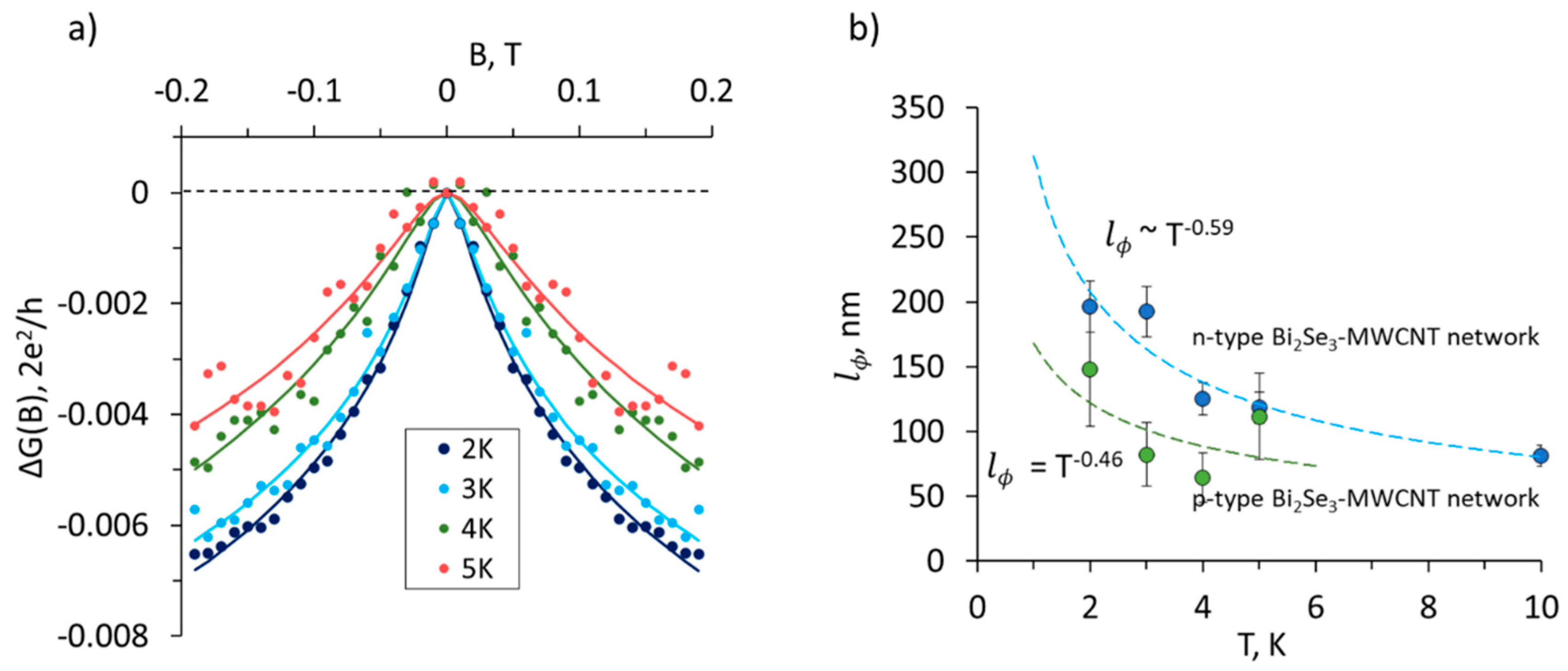
| T, K | p-Type Bi2Se3-MWCNT Network | n-Type Bi2Se3-MWCNT Network | ||
|---|---|---|---|---|
| lϕ, nm | α | lϕ, nm | α | |
| 2 | 148 | −0.02 | 197 | −0.02 |
| 3 | 82 | −0.1 | 192 | −0.021 |
| 4 | 64 | −0.1 | 125 | −0.025 |
| 5 | 111 | −0.02 | 118 | −0.024 |
| 10 | - | 82 | −0.023 | |
Disclaimer/Publisher’s Note: The statements, opinions and data contained in all publications are solely those of the individual author(s) and contributor(s) and not of MDPI and/or the editor(s). MDPI and/or the editor(s) disclaim responsibility for any injury to people or property resulting from any ideas, methods, instructions or products referred to in the content. |
© 2023 by the authors. Licensee MDPI, Basel, Switzerland. This article is an open access article distributed under the terms and conditions of the Creative Commons Attribution (CC BY) license (https://creativecommons.org/licenses/by/4.0/).
Share and Cite
Andzane, J.; Buks, K.; Spalva, E.; Felsharuk, A.; Erts, D. The Impact of Topological States on the Thermoelectric Performance of p- and n-Type Sb2Te3/Bi2Se3-Multiwalled Carbon Nanotubes Heterostructured Networks. Coatings 2023, 13, 2082. https://doi.org/10.3390/coatings13122082
Andzane J, Buks K, Spalva E, Felsharuk A, Erts D. The Impact of Topological States on the Thermoelectric Performance of p- and n-Type Sb2Te3/Bi2Se3-Multiwalled Carbon Nanotubes Heterostructured Networks. Coatings. 2023; 13(12):2082. https://doi.org/10.3390/coatings13122082
Chicago/Turabian StyleAndzane, Jana, Krisjanis Buks, Elmars Spalva, Andrei Felsharuk, and Donats Erts. 2023. "The Impact of Topological States on the Thermoelectric Performance of p- and n-Type Sb2Te3/Bi2Se3-Multiwalled Carbon Nanotubes Heterostructured Networks" Coatings 13, no. 12: 2082. https://doi.org/10.3390/coatings13122082