
Deposition and Characterisation of a Diamond/Ti/Diamond Multilayer Structure
 , , , , and
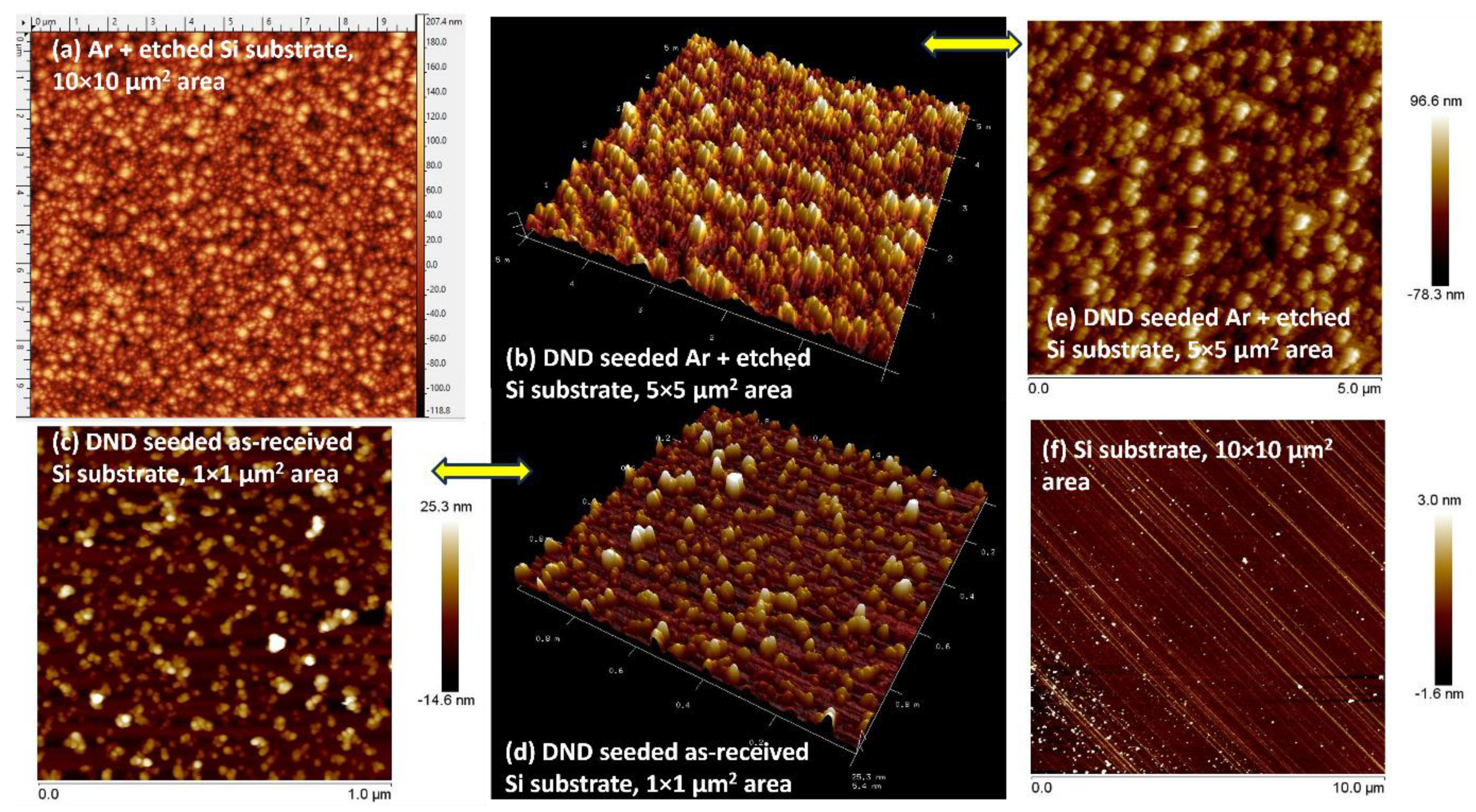
Abstract
:1. Introduction
2. Materials and Methods
2.1. Ar+ Ion Milling of the Base Substrate
2.2. DND Seeding of the Base Substrates
2.3. CVD of Microcrystalline Diamond (MCD)—Bottom Layer
2.4. PVD Sputtering of Ti Interlayer
2.5. Hydrogen Plasma Etching of Ti–Diamond Composite Double Layer
2.6. LAMWCVD of Nanocrystalline Diamond (NCD) Top Layer
2.7. Physical Characterisations
3. Results and Discussion
3.1. Base Substrate: Argon Plasma Etching and DND Seeding
3.2. First Layer of MCD Grown by LAMWCVD
3.2.1. LAMWCVD Growth Rate
3.2.2. Diamond Raman Signal
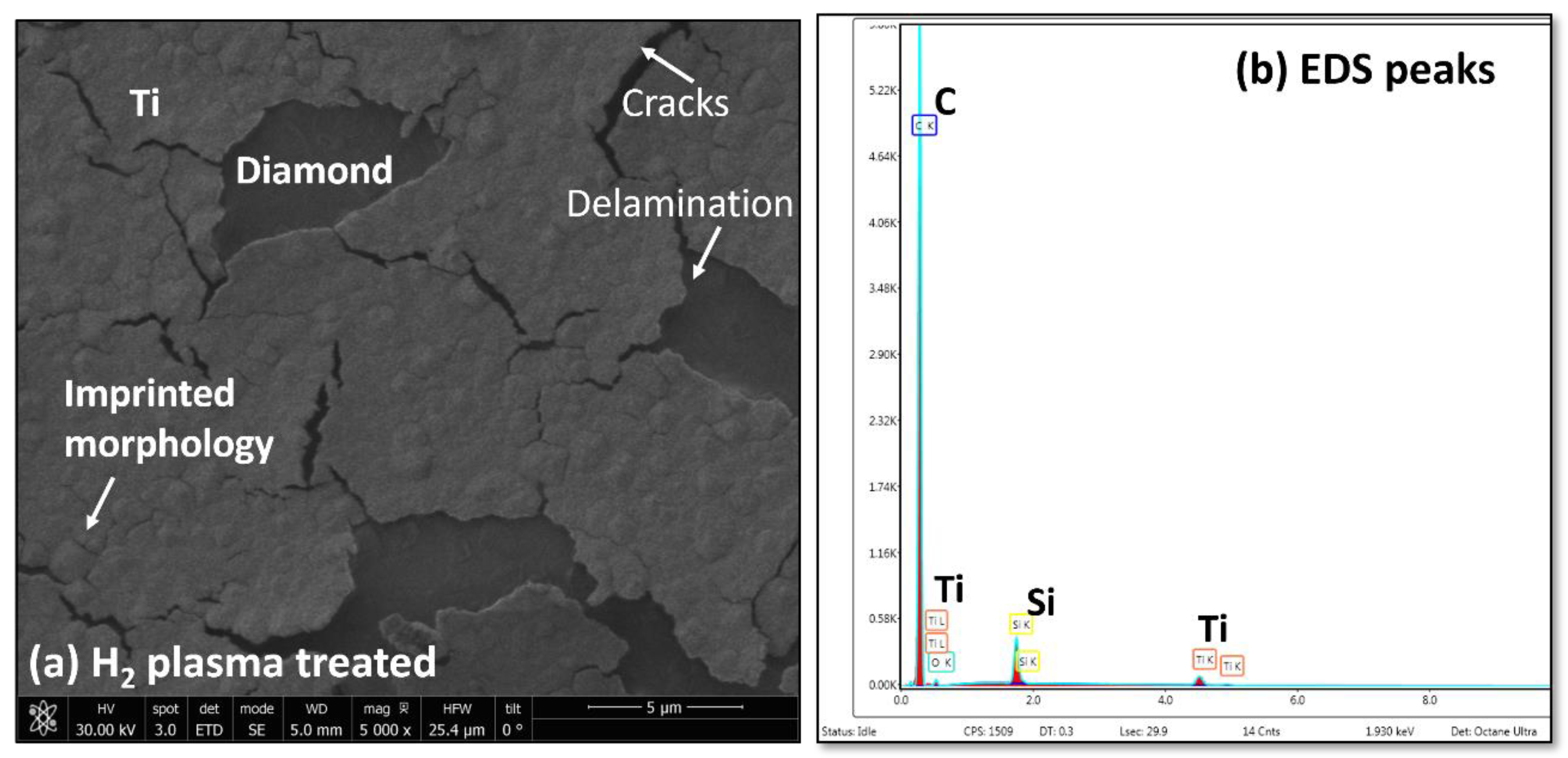
3.3. Ti PVD Sputtering and H2 Plasma-Etching of Ti-MCD Composite Layer
3.4. Top Layer NCD Grown by LAMWCVD
Diamond/Ti/Diamond Sandwich Structure: TEM Cross-Section
4. Conclusions
Author Contributions
Funding
Institutional Review Board Statement
Informed Consent Statement
Data Availability Statement
Acknowledgments
Conflicts of Interest
References
- Rats, D.; Vandenbulcke, L.; Herbin, R.; Benoit, R.; Erre, R.; Serin, V.; Sevely, J. Characterization of diamond films deposited on titanium and its alloys. Thin Solid Film. 1995, 270, 177–183. [Google Scholar] [CrossRef]
- Askari, S.; Chen, G.; Akhtar, F.; Lu, F. Adherent and low friction nanocrystalline diamond film grown on titanium using microwave CVD plasma. Diam. Relat. Mater. 2008, 17, 294–299. [Google Scholar] [CrossRef]
- Zhang, X.Y.; Ma, H.L.; Zhao, Y.M.; Yao, N.; Zeng, F.G.; Zhang, B.L. Comparative studies on field emission properties of diamond and diamond /Ti films. Adv. Mater. Res. 2012, 586, 177–180. [Google Scholar] [CrossRef]
- Veiga, C.; Davim, J.P.; Loureiro, A.J.R. Properties and applications of titanium alloys: A brief review. Rev. Adv. Mater. Sci. 2012, 32, 133–148. [Google Scholar]
- Sundfeldt, M.; Carlsson, L.V.; Johansson, C.B.; Thomsen, P.; Gretzer, C. Aseptic loosening, not only a question of wear: A review of different theories. Acta Orthop. 2006, 77, 177–197. [Google Scholar] [CrossRef]
- Rifai, A.; Tran, N.; Lau, D.W.; Elbourne, A.; Zhan, H.; Stacey, A.D.; Mayes, E.L.H.; Sarker, A.; Ivanova, E.P.; Crawford, R.J.; et al. Polycrystalline Diamond Coating of Additively Manufactured Titanium for Biomedical Applications. ACS Appl. Mater. Interfaces 2018, 10, 8474–8484. [Google Scholar] [CrossRef] [PubMed]
- Rifai, A.; Tran, N.; Reineck, P.; Elbourne, A.; Mayes, E.L.H.; Sarker, A.; Dekiwadia, C.; Ivanova, E.P.; Crawford, R.J.; Ohshima, T.; et al. Engineering the Interface: Nanodiamond Coating on 3D-Printed Titanium Promotes Mammalian Cell Growth and Inhibits Staphylococcus aureus Colonization. ACS Appl. Mater. Interfaces 2019, 11, 24588–24597. [Google Scholar] [CrossRef] [PubMed]
- Fox, K.; Mani, N.; Rifai, A.; Reineck, P.; Jones, A.; Tran, P.A.; Ramezannejad, A.; Brandt, M.; Gibson, B.C.; Greentree, A.D.; et al. 3D-Printed Diamond–Titanium Composite: A Hybrid Material for Implant Engineering. ACS Appl. Bio Mater. 2020, 3, 29–36. [Google Scholar] [CrossRef]
- Van Noort, R. Titanium: The implant material of today. J. Mater. Sci. 1987, 22, 3801–3811. [Google Scholar] [CrossRef]
- Zhao, L.; Chu, P.K.; Zhang, Y.; Wu, Z. Antibacterial coatings on titanium implants. J. Biomed. Mater. Res. Part B 2009, 91, 470–480. [Google Scholar] [CrossRef] [PubMed]
- Skoog, S.A.; Kumar, G.; Zheng, J.; Sumant, A.V.; Goering, P.L.; Narayan, R.J. Biological evaluation of ultrananocrystalline and nanocrystalline diamond coatings. J. Mater. Sci. Mater. Med. 2016, 27, 187. [Google Scholar] [CrossRef]
- Jana, A.; Dandapat, N.; Sengupta, S.; Balla, V.K.; Saha, R.; Mallik, A.K. Human osteoblast like MG63 cell and mouse fibroblast NIH3T3 cell viability study on the nucleation side of CVD grown polycrystalline diamond coatings. Trends Biomater. Artif. Organs 2015, 29, 211–216. [Google Scholar]
- Ahnood, A.; Meffin, H.; Garrett, D.J.; Fox, K.; Ganesan, K.; Stacey, A.; Apollo, N.V.; Wong, Y.T.; Lichter, S.G.; Kentler, W.; et al. Diamond Devices for High Acuity Prosthetic Vision. Adv. Biosyst. 2017, 1, 1600003. [Google Scholar] [CrossRef] [PubMed]
- Yan, B.; Loh, N.L.; Fu, Y.; Sun, C.Q.; Hing, P. Surface and interface characterization of diamond coatings deposited on pure titanium. Surf. Coat. Technol. 1999, 115, 256–265. [Google Scholar] [CrossRef]
- Kulesza, S.; Patyk, J.; Daenen, M.; Williams, O.; Van de Putte, W.; Fransaer, J.; Haenen, K.; Nesládek, M. Structural investigations of protective polycrystalline diamond coatings on titanium substrates. Surf. Coat. Technol. 2006, 201, 203–207. [Google Scholar] [CrossRef]
- Li, Y.; Yang, L.; Tang, Y.; Zhang, C.; Zhang, L.; Onyeka, I.; Yang, Q.; Feng, R.; Hirose, A. Adherent nanocrystalline diamond coatings deposited on Ti substrate at moderate temperatures. Surf. Coat. Technol. 2011, 206, 1971–1976. [Google Scholar] [CrossRef]
- Li, Y.; Zhang, C.; Ma, H.; Yang, L.; Zhang, L.; Tang, Y.; Li, X.; He, L.; Feng, R.; Yang, Q.; et al. CVD nanocrystalline diamond coatings on Ti alloy: A synchrotron-assisted interfacial investigation. Mater. Chem. Phys. 2012, 134, 145–152. [Google Scholar] [CrossRef]
- Li, X.; Li, Y.; He, L.; Yang, Q.; Hirose, A. Fine structures study of the diamond/titanium interface by transmission electron microscopy. Mater. Chem. Phys. 2014, 143, 647–652. [Google Scholar] [CrossRef]
- Zhang, C.; Niakan, H.; Yang, L.; Li, Y.; Hu, Y.; Yang, Q. Study of diamond nucleation and growth on Ti6Al4V with tungsten interlayer. Surf. Coat. Technol. 2013, 237, 248–254. [Google Scholar] [CrossRef]
- Fu, Y.; Yan, B.; Loh, N.L. Effects of pre-treatments and interlayers on the nucleation and growth of diamond coatings on titanium substrates. Surf. Coat. Technol. 2000, 130, 173–185. [Google Scholar] [CrossRef]
- Yang, B.; Li, H.; Yu, B.; Huang, N.; Liu, L.; Jiang, X. Deposition of highly adhesive nanocrystalline diamond films on Ti substrates via diamond/SiC composite interlayers. Diam. Relat. Mater. 2020, 108, 107928. [Google Scholar] [CrossRef]
- Wang, T.; Zhuang, H.; Jiang, X. One step deposition of highly adhesive diamond films on cemented carbide substrates via diamond/beta-SiC composite interlayers. Appl. Surf. Sci. 2015, 359, 790–796. [Google Scholar] [CrossRef]
- Lessiak, M.; Haubner, R. Diamond coatings on hardmetal substrates with CVD coatings as intermediate layers. Surf. Coat. Technol. 2013, 230, 119–123. [Google Scholar] [CrossRef]
- Fu, Y.; Loh, N.L.; Yan, B.; Sun, C.Q.; Hing, P. Control of microstructure coarsening of a Ti substrate during diamond film deposition using Ar/H-2/CH4 gas mixture. Thin Solid Film. 2000, 359, 215. [Google Scholar] [CrossRef]
- Tamburri, E.; Carcione, R.; Vitale, F.; Valguarnera, A.; Macis, S.; Lucci, M.; Terranova, M.L. Exploiting the Properties of Ti-Doped CVD-Grown Diamonds for the Assembling of Electrodes. Adv. Mater. Interfaces 2017, 4, 1700222. [Google Scholar] [CrossRef]
- Zhang, Y.; Wang, X.T.; Jiang, S.B.; Wu, J.H. Thermo-physical properties of Ti-coated diamond/Al composites prepared by pressure infiltration. Mater. Sci. Forum 2010, 654–656, 2572–2575. [Google Scholar] [CrossRef]
- Roy, S.; Das, M.; Mallik, A.K.; Balla, V.K. Laser melting of titanium-diamond composites: Microstructure and mechanical behavior study. Mater. Lett. 2016, 178, 284–287. [Google Scholar] [CrossRef]
- Liu, J.L.; Li, C.M.; Chen, L.X.; Zhang, Y.Y.; Hei, L.F.; Lv, F.X. Preparation and characterization of diamond-TiC-Ti-Ag/Cu gradient metallization system. Mater. Sci. Forum 2011, 687, 722–728. [Google Scholar] [CrossRef]
- Liu, D.; Zhou, Y.; Song, X.; Huo, W.; Feng, J. Interfacial microstructure and performance of nano-diamond film/Ti-6Al-4V joint brazed with AgCuTi alloy. Diam. Relat. Mater. 2016, 68, 42–50. [Google Scholar] [CrossRef]
- Chen, Y.; Su, H.H.; Fu, Y.C.; Guo, Z. Investigation of inferface microstructure of diamond and Ti coated diamond brazed with Cu-Sn-Ti alloy. Key Eng. Mater. 2011, 487, 199–203. [Google Scholar] [CrossRef]
- Jin, Y.; Wu, W.; Li, L.; Chen, J.; Zhang, J.; Zuo, Y.; Fu, J. Effect of sputtering power on surface topography of dc magnetron sputtered Ti thin films observed by AFM. Appl. Surf. Sci. 2009, 255, 4673–4679. [Google Scholar] [CrossRef]
- Wadge, M.D.; Turgut, B.; Murray, J.W.; Stuart, B.W.; Felfel, R.M.; Ahmed, I.; Grant, D.M. Developing highly nanoporous titanate structures via wet chemical conversion of DC magnetron sputtered titanium thin films. J. Colloid Interface Sci. 2020, 566, 271–283. [Google Scholar] [CrossRef] [PubMed]
- Zhang, L.; Shi, L.; He, Z.; Zhang, B.; Lu, Y.; Liu, A.; Wang, B. Deposition of dense and smooth Ti films using ECR plasma-assisted magnetron sputtering. Surf. Coat. Technol. 2009, 203, 3356–3360. [Google Scholar] [CrossRef]
- Chawla, V.; Jayaganthan, R.; Chawla, A.; Chandra, R. Microstructural characterizations of magnetron sputtered Ti films on glass substrate. J. Mater. Process. Technol. 2009, 209, 3444–3451. [Google Scholar] [CrossRef]
- Fontana, L.C.; Muzart, J.L.R. Characteristics of triode magnetron sputtering: The morphology of deposited titanium films. Surf. Coat. Technol. 1998, 107, 24–30. [Google Scholar] [CrossRef]
- Tankut, A.; Miller, K.E.; Ohuchi, F.S. PVD Ti-films for plasma-facing first walls, Part I: Characterization of surface chemistry during H2 and O2 exposure. J. Nucl. Mater. 2013, 433, 404–411. [Google Scholar] [CrossRef]
- Sha, X.; Yue, W.; Zhang, H.; Qin, W.; She, D.; Wang, C. Enhanced oxidation and graphitization resistance of polycrystalline diamond sintered with Ti-coated diamond powders. J. Mater. Sci. Technol. 2020, 43, 64–73. [Google Scholar] [CrossRef]
- Zhang, S.; Fu, Y.; Du, H.; Zeng, X.; Liu, Y. Magnetron sputtering of nanocomposite (Ti,Cr)CN/DLC coatings. Surf. Coat. Technol. 2003, 162, 42–48. [Google Scholar] [CrossRef]
- Liu, X.; Lu, P.; Wang, H.; Ren, Y.; Tan, X.; Sun, S.; Jia, H. Morphology and structure of Ti-doped diamond films prepared by microwave plasma chemical vapor deposition. Appl. Surf. Sci. 2018, 442, 529–536. [Google Scholar] [CrossRef]
- Qiang, L.; Zhang, B.; Zhou, Y.; Zhang, J. Improving the internal stress and wear resistance of DLC film by low content Ti Doping. Solid State Sci. 2013, 20, 17–22. [Google Scholar] [CrossRef]
- Drory, M.D.; Hutchinson, J.W. Diamond coating of Ti Alloys. Science 1994, 263, 1753. [Google Scholar] [CrossRef] [PubMed]
- Buccioni, E.; Braca, E.; Kenny, J.; Terranova, M. Processing–structure–adhesion relationship in CVD diamond films on titanium substrates. Diam. Relat. Mater. 1999, 8, 17–24. [Google Scholar] [CrossRef]
- Janssen, W.; Turner, S.; Sakr, G.; Jomard, F.; Barjon, J.; Degutis, G.; Lu, Y.-G.; D’Haen, J.; Hardy, A.; Van Bael, M.; et al. Substitutional phosphorus incorporation in nanocrystalline CVD diamond thin films. Phys. Status Solidi 2014, 8, 705–709. [Google Scholar] [CrossRef]
- Harniman, R.L.; Fox, O.J.; Janssen, W.; Drijkoningen, S.; Haenen, K.; May, P.W. Direct observation of electron emission from grain boundaries in CVD diamond by PeakForce-controlled tunnelling atomic force microscopy. Carbon 2015, 94, 386–395. [Google Scholar] [CrossRef]
- Pobedinskas, P.; Degutis, G.; Dexters, W.; Janssen, W.; Janssens, S.D.; Conings, B.; Ruttens, B.; D’Haen, J.; Boyen, H.-G.; Hardy, A.; et al. Surface plasma pretreatment for enhanced diamond nucleation on AlN. Appl. Phys. Lett. 2013, 102, 201609. [Google Scholar] [CrossRef]
- Pobedinskas, P.; Degutis, G.; Dexters, W.; D’haen, J.; Van Bael, M.; Haenen, K. Nanodiamond seeding on plasma-treated tantalum thin films and the role of surface contamination. Appl. Surf. Sci. 2021, 538, 148016. [Google Scholar] [CrossRef]
- Drijkoningen, S.; Pobedinskas, P.; Korneychuk, S.; Momot, A.; Balasubramaniam, Y.; Van Bael, M.K.; Turner, S.; Verbeeck, J.; Nesládek, M.; Haenen, K. On the origin of diamond plates deposited at low temperature. Cryst. Growth Des. 2017, 17, 4306. [Google Scholar] [CrossRef]
- Lloret, F.; Sankaran, K.J.; Millan-Barba, J.; Desta, D.; Rouzbahani, R.; Pobedinskas, P.; Gutierrez, M.; Boyen, H.-G.; Haenen, K. Improved Field Electron Emission Properties of Phosphorus and Nitrogen Co-Doped Nanocrystalline Diamond Films. Nanomaterials 2020, 10, 1024. [Google Scholar] [CrossRef]
- Rabinovich, Y.I.; Adler, J.J.; Ata, A.; Singh, R.K.; Moudgil, B.M. Adhesion between Nanoscale Rough Surfaces: I. Role of Asperity Geometry. J. Colloid Interface Sci. 2000, 232, 10–16. [Google Scholar] [CrossRef] [PubMed]
- Ferrari, A.C.; Robertson, J. Raman spectroscopy of amorphous, nanostructured, diamond–like carbon, and nanodiamond. Phil. Trans. R. Soc. A 2004, 362, 2477–2512. [Google Scholar] [CrossRef]
- Pal, K.S.; Mallik, A.K.; Dandapat, N.; Ray, N.R.; Datta, S.; Bysakh, S.; Guha, B.K. Microscopic properties of MPCVD diamond coatings studied by micro-Raman and micro-photoluminescence spectroscopy. Bull. Mater. Sci. 2015, 38, 537–549. [Google Scholar] [CrossRef]
- Degutis, G.; Pobedinskas, P.; Turner, S.; Lu, Y.-G.; Al Riyami, S.; Ruttens, B.; Yoshitake, T.; D’Haen, J.; Haenen, K.; Verbeeck, J.; et al. CVD diamond growth from nanodiamond seeds buried under a thin chromium layer. Diam. Relat. Mater. 2016, 64, 163–168. [Google Scholar] [CrossRef]
- Daenen, M.; Zhang, L.; Erni, R.; Williams, O.A.; Hardy, A.; Van Bael, M.K.; Wagner, P.; Haenen, K.; Nesládek, M.; Van Tendeloo, G. Diamond nucleation by carbon transport from buried nanodiamond TiO2 sol-gel composites. Adv. Mater. 2009, 21, 670–673. [Google Scholar] [CrossRef]
- Lu, Y.-G.; Verbeeck, J.; Turner, S.; Hardy, A.; Janssens, S.D.; De Dobbelaere, C.; Wagner, P.; Van Bael, M.K.; Haenen, K.; Van Tendeloo, G. Analytical TEM study of CVD diamond growth on TiO2 sol-gel layers. Diam. Relat. Mater. 2012, 23, 93–99. [Google Scholar] [CrossRef]
- Sankaran, K.J.; Yeh, C.-J.; Hsieh, P.-Y.; Pobedinskas, P.; Kunuku, S.; Leou, K.-C.; Tai, N.-H.; Lin, I.-N.; Haenen, K. Origin of Conductive Nanocrystalline Diamond Nanoneedles for Optoelectronic Applications. ACS Appl. Mater. Interfaces 2019, 11, 25388–25398. [Google Scholar] [CrossRef] [PubMed]


Disclaimer/Publisher’s Note: The statements, opinions and data contained in all publications are solely those of the individual author(s) and contributor(s) and not of MDPI and/or the editor(s). MDPI and/or the editor(s) disclaim responsibility for any injury to people or property resulting from any ideas, methods, instructions or products referred to in the content. |
© 2023 by the authors. Licensee MDPI, Basel, Switzerland. This article is an open access article distributed under the terms and conditions of the Creative Commons Attribution (CC BY) license (https://creativecommons.org/licenses/by/4.0/).
Share and Cite
Mallik, A.K.; Lloret, F.; Gutierrez, M.; Rouzbahani, R.; Pobedinskas, P.; Shih, W.-C.; Haenen, K. Deposition and Characterisation of a Diamond/Ti/Diamond Multilayer Structure. Coatings 2023, 13, 1914. https://doi.org/10.3390/coatings13111914
Mallik AK, Lloret F, Gutierrez M, Rouzbahani R, Pobedinskas P, Shih W-C, Haenen K. Deposition and Characterisation of a Diamond/Ti/Diamond Multilayer Structure. Coatings. 2023; 13(11):1914. https://doi.org/10.3390/coatings13111914
Chicago/Turabian StyleMallik, Awadesh Kumar, Fernando Lloret, Marina Gutierrez, Rozita Rouzbahani, Paulius Pobedinskas, Wen-Ching Shih, and Ken Haenen. 2023. "Deposition and Characterisation of a Diamond/Ti/Diamond Multilayer Structure" Coatings 13, no. 11: 1914. https://doi.org/10.3390/coatings13111914