1. Introduction
Organic–inorganic hybrid perovskite solar cells (PSCs) are emerging photovoltaic devices considered to have good application prospects owing to their characteristics, such as high extinction coefficients [
1], long carrier lifetimes [
2], long carrier diffusion lengths [
3,
4], adjustable band gap, and defect tolerance [
5,
6]. Furthermore, the photoelectric conversion efficiency (PCE) of perovskite solar cells has improved from 3.8% to 26.1% in recent years [
7,
8]. However, further improving the PCE and the environmental stability of PSCs has garnered more and more attention from researchers worldwide.
A high density of defect states exists on the surfaces and grain boundaries of perovskite grains. Their energy disorder and reduced carrier concentrations seriously affect the PCE of a device [
9]. In addition, these defects may cause problems such as ion migration and related current hysteresis, as well as the degradation of the device due to environmental factors, especially in the case of lead-free perovskite solar cells [
10,
11]. Therefore, high-quality perovskite films with large crystal sizes and a reduced grain boundary density are necessary for efficient and stable solar cells. Several methods have been developed to fabricate large-grain-size perovskite films. Compared with physical fabrication methods (e.g., solvent annealing [
12], air blowing [
13], and hot casting [
14]), chemical methods (e.g., solvent-based solvent engineering [
15] and additive engineering) are more straightforward and more controllable. Wu et al. added H
2O as an additive to a two-step PbI
2/dimethylformamide (DMF) precursor solution to increase the grain size of the perovskite film to 1 μm [
16]. After the perovskite film was annealed in the DMF steam, a single-layer perovskite film with a grain size of 3 μm was obtained and the filling factor reached 83%. Deng et al. studied the formation of the adduct mesophase in the precursor solution and its effect on the performance of the perovskite films by adjusting the dimethyl sulfoxide (DMSO) and DMF ratio in the mixed cationic perovskite one-step precursor solution [
17]. They fabricated a perovskite film with a crystal size of 500 nm with a 3:5 volume ratio of DMSO and DMF. Sun et al. used ethyl ammonium chloride as an additive to the one-step perovskite precursor solution to obtain a high-quality perovskite film with a 3 μm crystal size, which improved carrier lifetime, reduced defect density, and increased the electrical conductivity and charge mobility of the material [
18].
Dai et al. incorporated CsPbBr
3 nanoparticles into the chlorobenzene anti-solvent of PSC. Inorganic perovskite nanostructures were used to control the growth of perovskite films to improve crystallinity, increase grain size (1–2 μm), and reduce defects [
19]. As a result, a double-layer perovskite film of Cs
1−yMA
yPbI
3−xBr
x and MAPbI
3 was formed, which improved charge collection and increased stability. Generally, perovskite films prepared via a one-step method, including solvent engineering using an anti-solvent, such as chlorobenzene, have a smaller grain size. However, the small grain size is accompanied by a significant number of defects caused by grain boundaries, which enhance carrier recombination and hinder carrier transport [
20,
21]. In contrast, sequential deposition has higher controllability on the morphology and size of crystals, which can reproducibly prepare perovskite films composed of larger-sized crystal grains.
In this paper, we report a method that replaces a part of PbI
2 with PbCl
2 and MACl in the sequential deposition step solution. After anti-solvent extraction and annealing, a PbI
2 film with a small amount of MAPbCl
3 crystals was formed. After the MAI solution was spin-coated in the second step, the growth of the perovskite film was induced via the addition of MAPbCl
3 crystals. Compared with pure perovskite films, MAPbCl
3-induced perovskite films had superior film quality, larger grain size, and reduced defect state density, significantly extending the carrier lifetime.
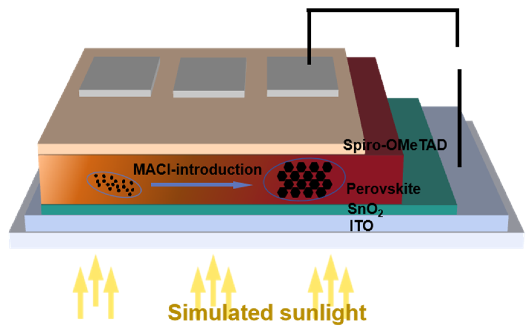
Figure 1 shows the structure of PSCs and the influence of the MACl on the microstructure of perovskite films. The optimized device using the MAPbCl
3-induced perovskite film showed a PCE of 20.97%, which has good stability and effectively inhibits the hysteresis.
2. Experimental Details
2.1. Materials
N-dimethylformamide (DMF, 99.8%, Sigma-Aldrich, St. Louis, MO, USA); dimethyl sulfoxide (DMSO, 99.5%, Sigma-Aldrich); anhydrous isopropanol (IPA, 99.5%, Sigma-Aldrich, St. Louis, MO, USA); chlorobenzene (CB, 99.8%, Sigma-Aldrich, St. Louis, MO, USA); Acetonitrile (CAN, 99.9%, Sigma-Aldrich, St. Louis, MO, USA); PbI2 (99.999%, Xi’an Polymer Light Technology Corp., Xi’an, China); PbCl2 (99.999%, Xi’an Polymer Light Technology Corp.); CH3NH3I (MAI, 99.5%, Xi’an Polymer Light Technology Corp., Xi’an, China); CH3NH3Cl (MACl, 99.5%, Xi’an Polymer Light Technology Corp., Xi’an, China); Spiro-OMeTAD (99.98%, Xi’an Polymer Light Technology Corp., Xi’an, China); lithium bis(trifluoromethanesulfonyl)imide salt (Li-TFSI, 99.95%, Sigma-Aldrich); 4-tert-butylpyridine (tBP, >96.0%, Sigma-Aldrich, St. Louis, MO, USA); urea (Sinopharm Chemical Reagent Co., Ltd., Shanghai, China); HCl (Sinopharm Chemical Reagent Co., Ltd., Shanghai, China); mercaptoacetic acid (Sinopharm Chemical Reagent Co., Ltd., Shanghai, China); SnCl2·2H2O (98%, Alfa Aesar, Ward Hill, MA, USA); SnO2 (SnO2 15% in H2O colloidal dispersion, Alfa Aesar, Ward Hill, MA, USA); gold electrode (99.99%, Zhongnuo Advanced Material Technology Co., Ltd., Beijing, China).
2.2. Preparation of Precursor Solutions
The PbI2 precursor solution was prepared by a conventional two-step process. The solvent used in the precursor solution was composed of 0.8 mL of DMF and 0.2 mL of DMSO. PbI2, PbCl2, and MACl were added to 1 mL of the solvent in ratios of 1:0:0, 0.9:0.1:0.1, 0.8:0.2:0.2, and 0.7:0.3:0.3, with the total Pb2+ solubility being 1M. The mixture was dissolved by magnetic stirring to prepare a precursor solution required for the experiment. The second step of solution preparation was to add 39.75 mg of MAI to 1 mL of the IPA solvent and dissolve it by magnetic stirring to obtain a solution with a molar concentration of 0.25 M MAI. The HTM Spiro-OMeTAD solution was prepared by dissolving 72.3 mg of Spiro-OMeTAD in 1 mL of the CB solvent, adding 17.5 μL of the Li-TFSI solution (520 mg of Li-TFSI dissolved in 1 mL of ACN) and 28.8 μL of tBP, and dissolving with magnetic stirring. After 12 h, all solutions were filtered using a 0.44-μm-pore polyvinylidene difluoride syringe filter.
2.3. Device Fabrication
A 25 mm × 25 mm glass with ITO coating was ultrasonically washed separately with deionized water, acetone, and alcohol for 15 min. After N2 drying, it was put in an ultraviolet (UV) radiation machine for 30 min of ultraviolet ozone treatment. Electron transport layers were prepared in two steps: spin coating and water bath. The 15% SnO2 hydrocolloid solution and H2O were diluted at a ratio of 1:4 to obtain a 3% SnO2 hydrocolloid solution. It was spin-coated on clean ITO glass for 30 s at 3000 rpm. The sample was then annealed on a heating stage at 180 °C for 40 min. The water bath solution was dissolved in 80 mL of deionized water with 1 g of urea, and 20 μL of thioglycolic acid, 0.5 mL of HCl solution, and 0.01 M SnCl2·2H2O were added. After stirring the water bath solution for 10 min, it was heated to 70 °C and maintained at this temperature. The sample was placed vertically in the water bath solution for 3 h. After being dried with N2, the sample was placed on a heating table at 180 °C for 1 h. Next, the sample was placed in a glove box.
The first step in the deposition of the perovskite film was to apply 120 μL of the precursor solution to a SnO2 substrate and spin coat at 3000 rpm for 30 s. Next, 200 μL of anti-solvent CB was added dropwise during the last few seconds of the spin coating process to accelerate the crystallization process. The wet film was annealed on a heating stage at 60 °C for 2 min to obtain a PbI2 film. After the temperature was lowered, the second step of the spin coating was performed. Here, 120 μL of the second step solution was spin-coated on the sample at 3000 rpm for 30 s. The sample was then annealed on a hot plate at 100 °C for 30 min to obtain a perovskite film. After the temperature was lowered, 100 μL of Spiro solution was spin coated, at 4000 rpm for 30 s, on the surface of the perovskite film. The sample was placed in a dry box and oxidized for 12 h in an environment with a Relative Humidity (RH) of <10%. Finally, a Au electrode of approximately 50 nm was deposited by thermal evaporation at a pressure of 3 × 10⁻⁶ Pa.
2.4. Characterization
Scanning electron microscope (SEM) images were collected by Hitachi S-4800. Atomic force microscopy (AFM) images were obtained using an MFP-3D Infinity AFM (Asylum Research, Oxford Instruments, Oxford, UK). The X-ray diffraction (XRD) patterns of the films in the 10°−50° region were collected by a Bruker D8 X-ray diffractometer with CuKa radiation (1.5418 Å) at a scan rate of 4°/min. The absorption spectra of the films were measured with a Hitachi U-4100 UV-Vis spectrophotometer (Hitachi, Tokyo, Japan). X-ray photoelectron spectroscopy (XPS) data were obtained by an ESCALab220i-XL electron spectrometer from VG Scientific (Thermo Fisher Scientific, Waltham, MA, USA). The test samples of SEM images, AFM images, XRD diffraction patterns, absorption spectra, and XPS data were fabricated in a glass/ITO/SnO2/Perovskite planar device architecture. Photospectral response was measured by an external quantum efficiency (EQE) measurement system (QEX10, PV Measurement, Boulder, CO, USA). The photoluminescence (PL) spectra of samples were recorded by the Edinburgh Instrument FLS920, and the excitation light source was a 450 W xenon lamp. The time-resolved photoluminescence (TRPL) spectra were measured by Edinburgh Instrument FLS920 (Livingston, UK), and the excitation light source was a 470 nm pulsed laser beam. The J-V curves under AM1.5 illumination (standard 100 mW∙cm−2) of the devices with perovskite films were measured by Agilent B1500A Semiconductor parameter analysis instrument (Keysight, Santa Rosa, CA, USA), and the light source was a 450W xenon lamp.
3. Results and Discussion
In sequential deposition, PbI
2 in the precursor solution was replaced with PbI
2, PbCl
2, and MACl; the ratios were 1:0:0, 0.9:0.1:0.1, 0.8:0.2:0.2, and 0.7:0.3:0.3. In the first step of the sequential deposition process, a trace amount of MAPbCl
3 crystals in the PbI
2 film formed after a short annealing time because PbCl
2 and MACl were added to the solution. In the XRD pattern of the PbI
2 film, as shown in
Figure S1, the diffraction peak of MAPbCl
3 at 15.6° can be observed. At the same time, a weak diffraction peak of MAPbI
3 at 14.2° can be observed, possibly due to the conversion of a small amount of Cl
− into other chlorinated compounds.
Figure S1 shows the XRD and top-view SEM images of pure PbI
2 and PbI
2 films containing MAPbCl
3. As the proportion of PbCl
2 and MACl increased, the content of MAPbCl
3 in the PbI
2 film increased. Moreover, a trace amount of MAPbCl
3 crystals changed the morphology of the PbI
2 film, making it appear as a rod-like structure.
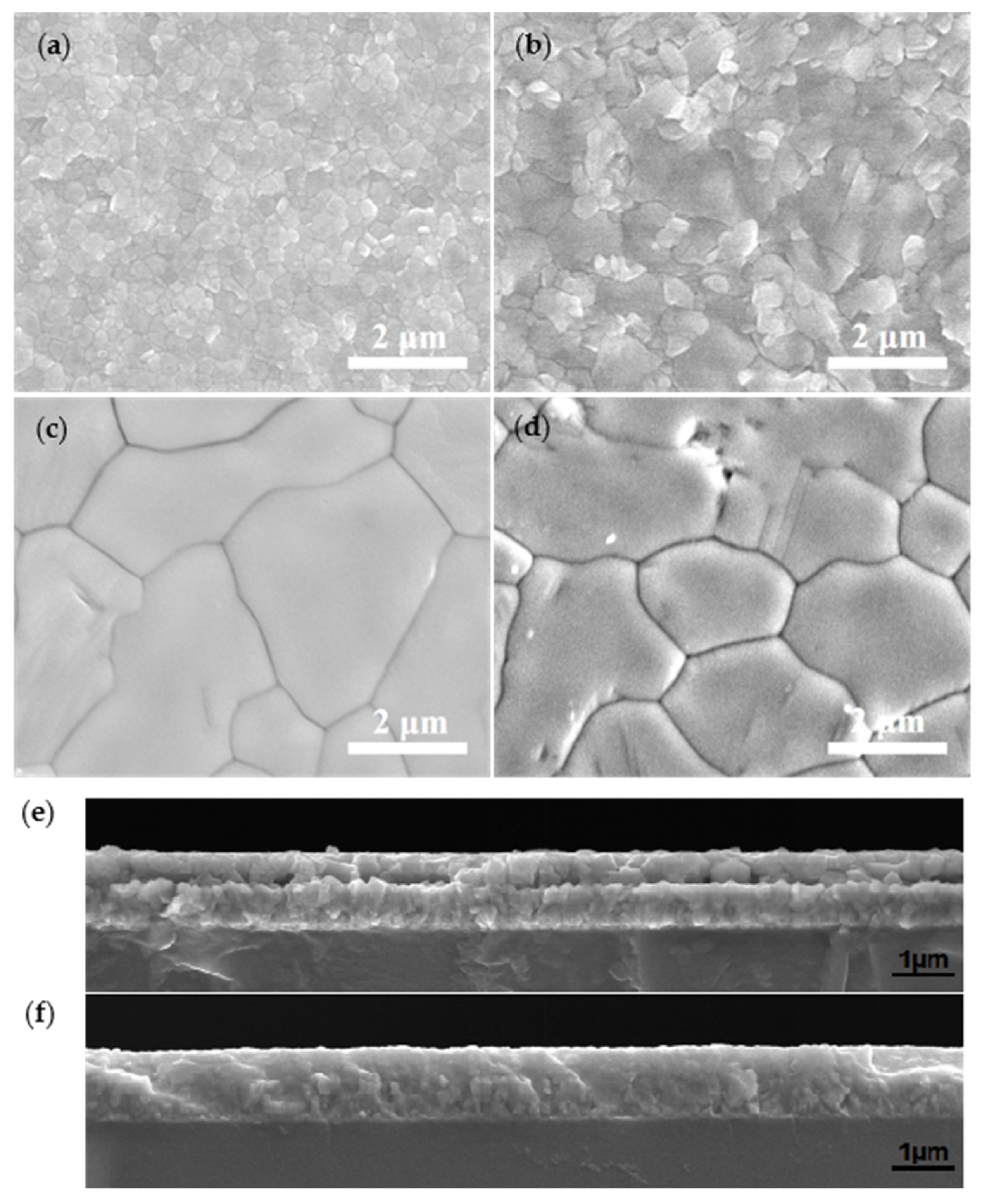
In the second step of spin coating, we used the MAI solution, and then annealing was performed to obtain a perovskite film. The effect of trace amounts of MAPbCl
3 crystals in the PbI
2 film on the morphology of the perovskite film can be observed in
Figure 2a–d, which shows top-down SEM images of perovskite films prepared with different ratios of precursor solutions. It can be observed that the pure perovskite film exhibits a uniform morphology. However, the average grain size is only 300 nm. It is worth noting that a significant number of grain boundaries is detrimental to carrier collection and transportation [
12,
22]. However, the crystal sizes of MAPbCl
3-induced perovskite films are significantly increased. The crystal size of the perovskite film prepared from the precursor solution of PbI
2:PbCl
2:MACl (0.8:0.2:0.2) reached approximately 3 μm, as shown in
Figure 2c. The MAPbCl
3 crystal in the PbI
2 film becomes a nucleation site of the perovskite film like a seed after the MAI solution is spin coated, thereby promoting the crystal growth of perovskite. As shown in
Figure 2d, a small number of high-brightness grains and voids appeared in the perovskite film prepared from the precursor solution with a ratio of 0.7:0.3:0.3. This shows that the induction of an appropriate amount of MAPbCl
3 crystals can produce a perovskite film with a large crystal size and few grain boundaries. The SEM cross-sectional image of the films (
Figure 2e,f) showed the same results.
Then, the AFM measurements were performed to study the influence of MAPbCl
3 crystals on the morphology of perovskite films (in
Figure S2). Compared with the pure perovskite film (21.9 nm), the surface roughness of the perovskite film prepared with the PbI
2:PbCl
2:MACl (0.8:0.2:0.2) precursor solution (13.2 nm) is relatively reduced. Consistent with the observation results of the previous SEM images, an increase in the grain size of the perovskite film induced by MAPbCl
3 was also observed in the AFM image. A lower roughness indicates a smoother surface with fewer voids and grain boundaries, which improves carrier extraction.
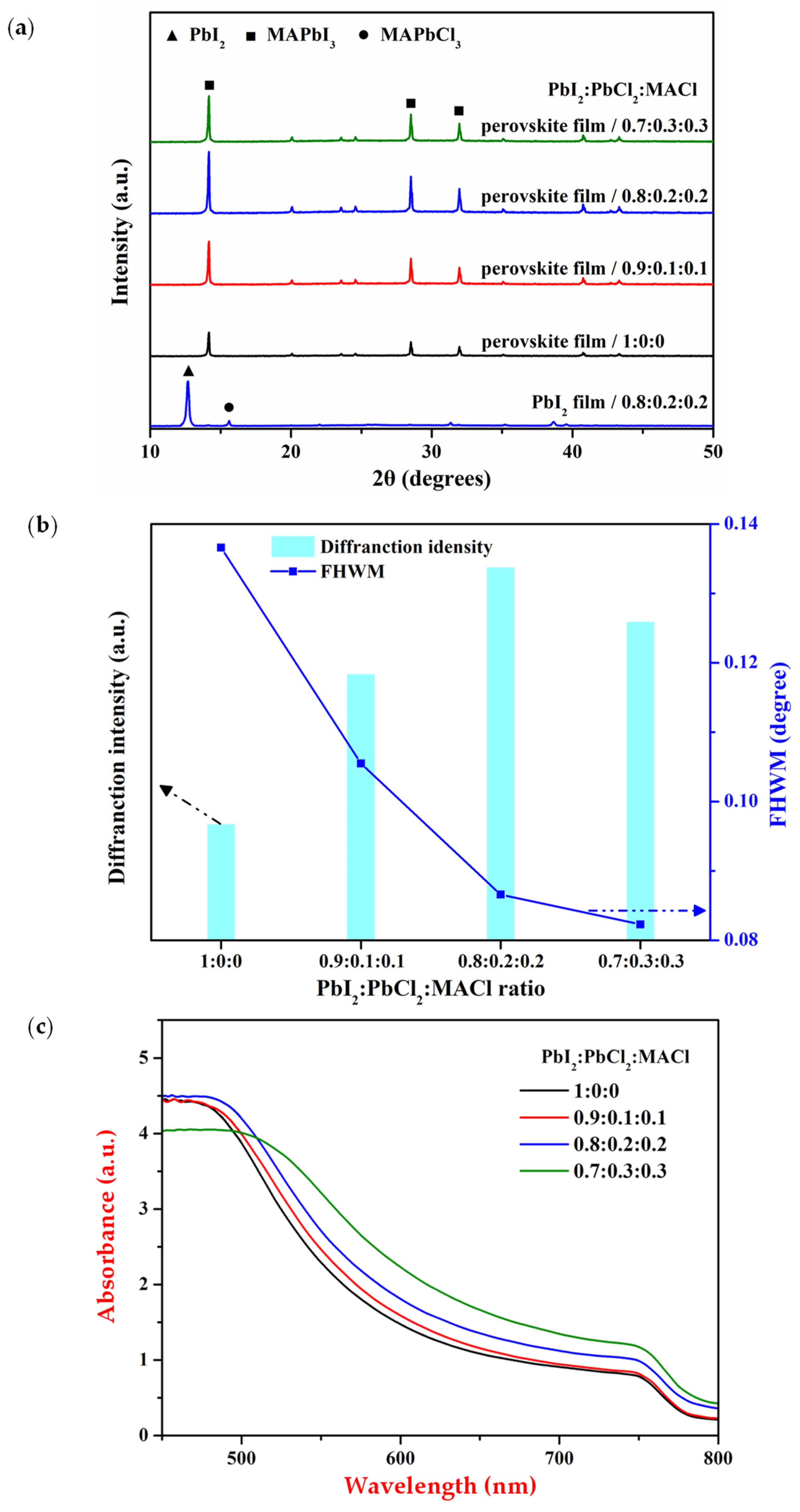
XRD patterns can confirm the composition and quality of perovskite films induced by MAPbCl
3. The diffraction peaks of all perovskite films are located at 14.1°, 28.3°, and 31.9°, corresponding to the (110), (220), and (319) crystal planes of the tetragonal MAPbI
3, as shown in
Figure 3a. This indicates that the phase and crystal structure of the perovskite film will not change with the addition of MAPbCl
3. Note that the diffraction peak of MAPbCl
3 at 15.6° cannot be observed, which indicates that MAPbCl
3 leaves almost no residue. To test this hypothesis, we utilized X-ray photoelectron spectroscopy (XPS). The MAPbCl
3-induced perovskite film has a significantly weak chlorine content, as shown in
Figure S3. This is due to the lower thermal stability exhibited by MAPbCl
3 compared with MAPbI
3 during the growth of the perovskite film. The MAPbCl
3 phase decomposes and releases MACl, which is due to excess MAI replacing MAPbI
3 or MAPbI
3−xCl
x [
23]. The decomposed MACl eventually sublimates, reducing the perovskite film’s Cl content [
24]. The intensities and full width at half maxima (FWHM) of the 14.1° diffraction peak of the perovskite films fabricated with different ratios of precursor solutions are shown in
Figure 3b. The increase in the diffraction peak intensity indicates that the MAPbCl
3-induced perovskite film has excellent crystallinity, whereas a decrease in the FWHM value indicates an increase in grain size, which is consistent with the SEM image in
Figure 1. The increase in the (110) peak intensity and decrease in the FWHM value indicates that the introduction of an appropriate amount of MAPbCl
3 in the sequential deposition process can regulate the nucleation and crystallization process of the perovskite film, resulting in a significant increase in the crystallinity and crystal size of the perovskite film. When the ratio of PbI
2: PbCl
2: MACl is 0.7: 0.3: 0.3, the intensity of the (110) diffraction peak decreases. The MAPbCl
3 crystals in the PbI
2 film will accelerate the growth of the perovskite film. The too-high content of MAPbCl
3 will cause the perovskite film to grow too fast, reducing the crystallinity and (110) preferential orientation.
We further studied the optical properties of MAPbCl
3-induced perovskite films using UV-visible absorption spectroscopy. The UV-vis absorption spectra of perovskite films prepared from precursor solutions containing various PbI
2:PbCl
2:MACl ratios are shown in
Figure 3c. The light absorption of the perovskite film increases with the increase in MAPbCl
3 (proportion of PbCl
2 and MACl). This can be attributed to the better crystallinity due to the induction of MAPbCl
3, which leads to enhanced light absorption in the long-wave region (from 500 nm to 1000 nm). When the PbI
2:PbCl
2:MACl ratio is 0.7:0.3:0.3, the light absorption of the perovskite film in the short-wave region (from 450 nm to 500 nm) is significantly reduced, indicating that there are a lot of nano-scale voids in the film, which is consistent with the results shown in
Figure 2d.
To evaluate the photovoltaic performance of MAPbCl
3-induced high-quality perovskite film devices, we fabricated the PSC devices with a structure of glass/ITO/SnO
2/Perovskite/Spiro-OMeTAD/Au. To ensure the reliability of the experimental data, 20 devices were manufactured for each precursor solution of the PbI
2:PbCl
2:MACl ratio.
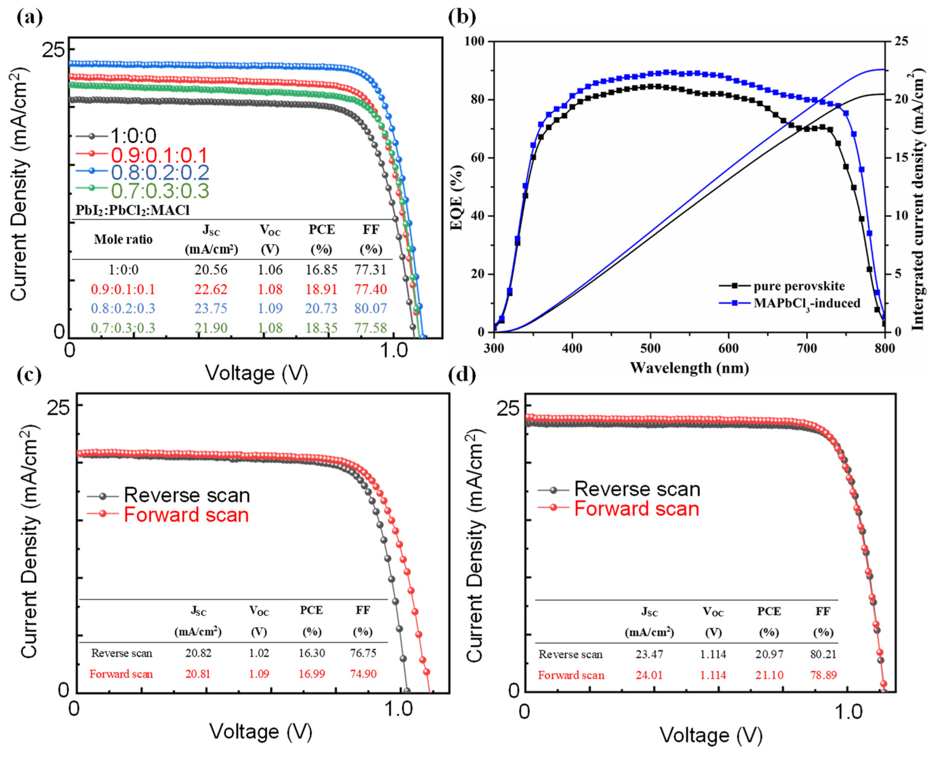
Figure 4a shows the champion PCE curve of the device prepared by the precursor solution of each PbI
2:PbCl
2:MACl ratio. It can be seen that with an increase in the ratio of PbCl
2 and MACl, the PCE of PSC primarily increases and then decreases, reaching a maximum value at 0.8:0.2:0.2. The PCE of the pristine perovskite device was 16.85%, with the
of 20.56 mA/cm
2, the
of 1.06 V, and the FF of 77.31%; while the PCE of the optimized perovskite device (0.8:0.2:0.2) was 20.97%, with the
of 23.47 mA/cm
2, the
of 1.114 V, and the FF of 80.21%. It can be seen that the photovoltaic parameters of optimized perovskite devices improved and the PCE increased by at least 23%.
Figure S4 shows the distribution of photovoltaic parameters of perovskite solar cells. Compared with the reference, the value of
and FF was higher and its distribution was more concentrated. As a result, after adding the MACl in the precursor solution, the PCE of PSCs has been enhanced.
Figure 4b shows the EQE spectra of the pure perovskite and MAPbCl
3-induced devices. The device prepared using optimized MAPbCl
3-induced perovskite has a better photoelectric response and remains above 80% in the wavelength region between 394 nm and 701 nm. The MAPbCl
3-induced film shows high injection photon conversion efficiency in this region, which is attributed to the stronger light absorption of the film in this region, as shown in
Figure 2c. Integrating the EQE spectra, respectively, the obtained current densities showed the same trend with the
values of the pure perovskite and MAPbCl
3-induced devices.
Figure 4c,d shows the
J-V hysteresis curves of the pure perovskite and MAPbCl
3-induced devices, respectively. Therefore, adding MAPbCl
3 to the solution can effectively reduce hysteresis, which indicates suppressed ion migration. Since grain boundaries are the main channels for ion migration, increased grain size and reduced grain boundaries of the MAPbCl
3-induced perovskites lead to suppressed ion migration and reduced hysteresis [
25,
26].
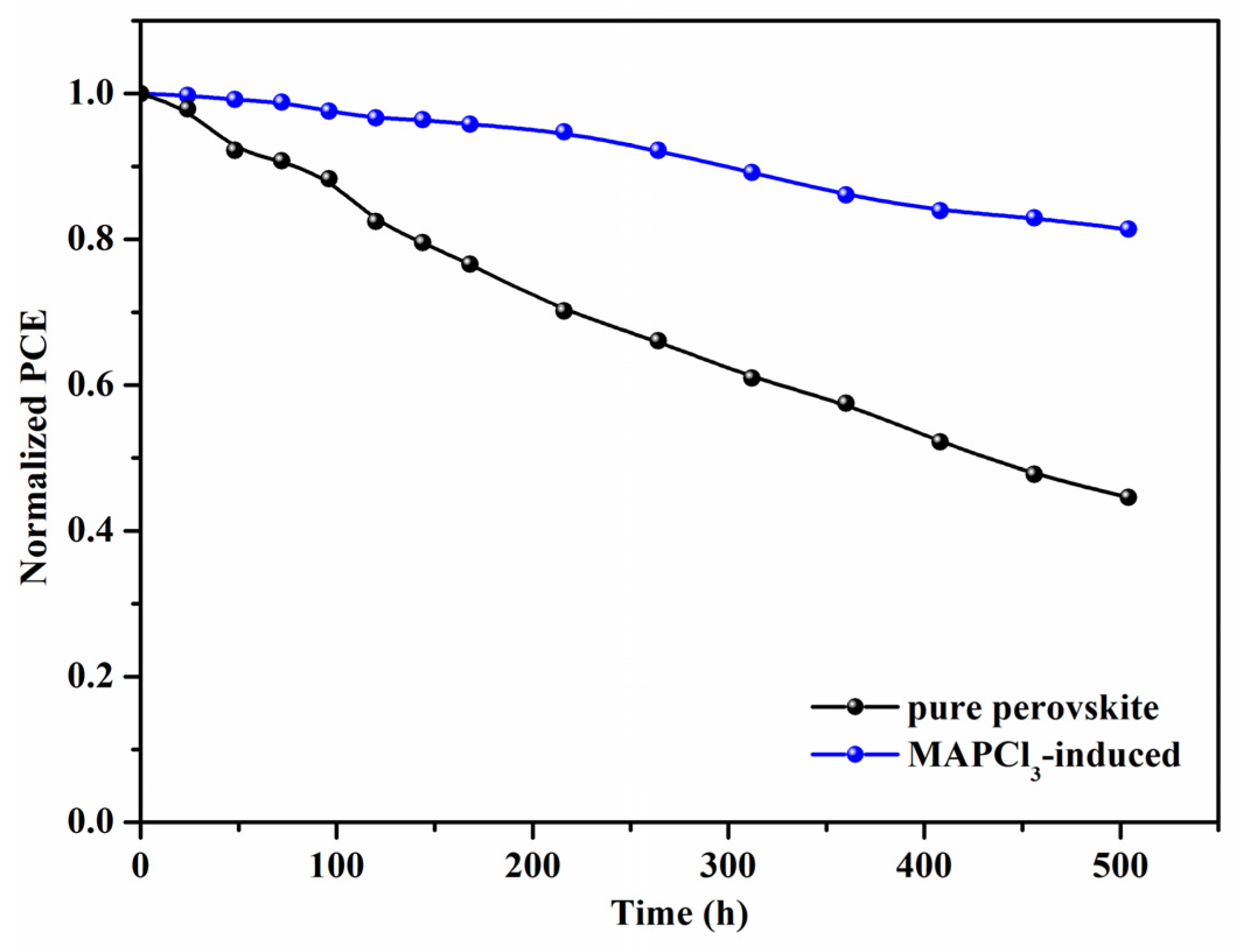
Compared with pure perovskite devices, the devices induced by MAPbCl
3 show a more stable power output and faster optical response. This quick optical response reflects efficient carrier extraction and reduced carrier recombination. In addition, ten independent devices were subjected to an aging experiment for more than 500 h to test the stability of the MAPbCl
3-induced PSCs. PSCs were stored in the air at a relative humidity of 20%–30% and were not encapsulated in the dark. For comparison, ten pure perovskite devices were tested in the same environment. The change in PCE over time is shown in
Figure 5. Compared with 45% of the original properties of pure devices, MAPbCl
3-induced PSCs show significant stability in the surrounding atmosphere and retain more than 80% of the original PCE after 500 h of storage. Since the degradation of perovskite was mainly caused by water entering the perovskite film along the grain boundaries [
27], reduced grain boundary density by increased crystal grain size and the improved crystal quality can enhance the stability of MAPbCl
3-induced devices.
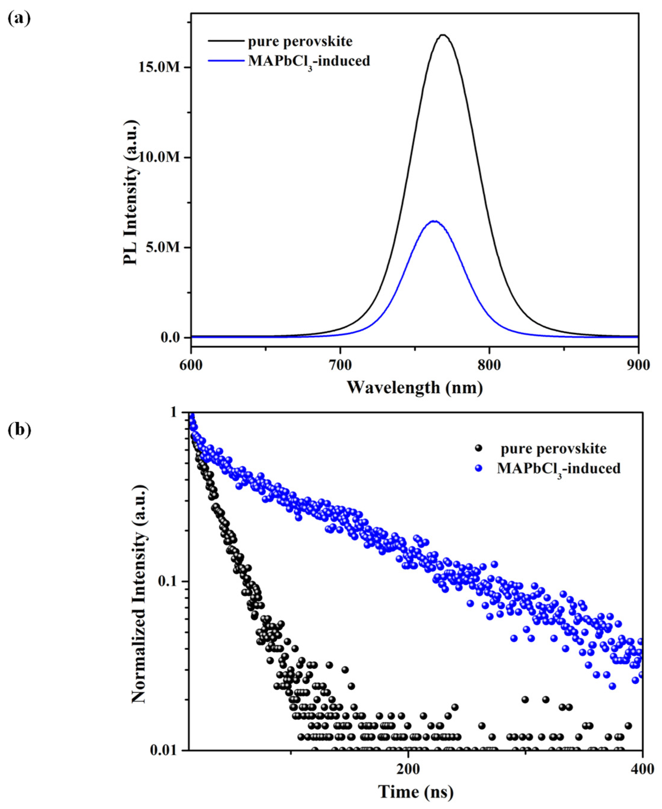
Some optical and electrical measurements were performed to further study the mechanism of MAPbCl
3 induction to improve the properties of perovskite films.
Figure 6a shows the PL spectra of pure perovskite and MAPbCl
3-induced films on glass/ITO/SnO
2 substrate. The induction of MAPbCl
3 reduces the defect state and crystal disorder in the perovskite thin film, leading to fewer defect states and better crystal distribution. This results in a significant decrease in the PL strength of perovskite. In addition, the PL emission peak is slightly blue-shifted because of trace residual Cl.
Furthermore, after normalizing the PL spectrum (
Figure S5), it was found that the MAPbCl
3-induced perovskite film has a narrower FWHM than that of pure perovskite. This also shows that MAPbCl
3 reduces the film’s defect content due to enhanced crystallinity.
Figure 6b shows the time-resolved PL (TRPL) of pure perovskite and MAPbCl
3-induced films. The data were fitted using the following double exponential equation [
28]. The results are shown in
Table 1.
A1 and
A2 represent the contributions of the fast and slow components;
τ1 and
τ2 represent decay lifetime. From
Table 1, the fluorescence quenching of the
component is severe, indicating less nonradiative recombination caused by surface or body defects. The rapid decay constant (
τ1) indicates the carrier extraction. The fluorescence decay of the
component is slower, reflecting the radiation recombination in perovskite. The slow decay constant (
τ2) represents the radiation recombination [
29,
30]. Adding MAPbCl
3 significantly reduces the proportion of nonradiative recombination, indicating the low carrier trap state density [
31]. Similarly, the reduced
and increased
of the MAPbCl
3-induced film indicate that the large-grained perovskite film prepared using MAPbCl
3 can make carriers transfer to the transport layer faster. Furthermore, the carrier diffusion length is longer [
32].
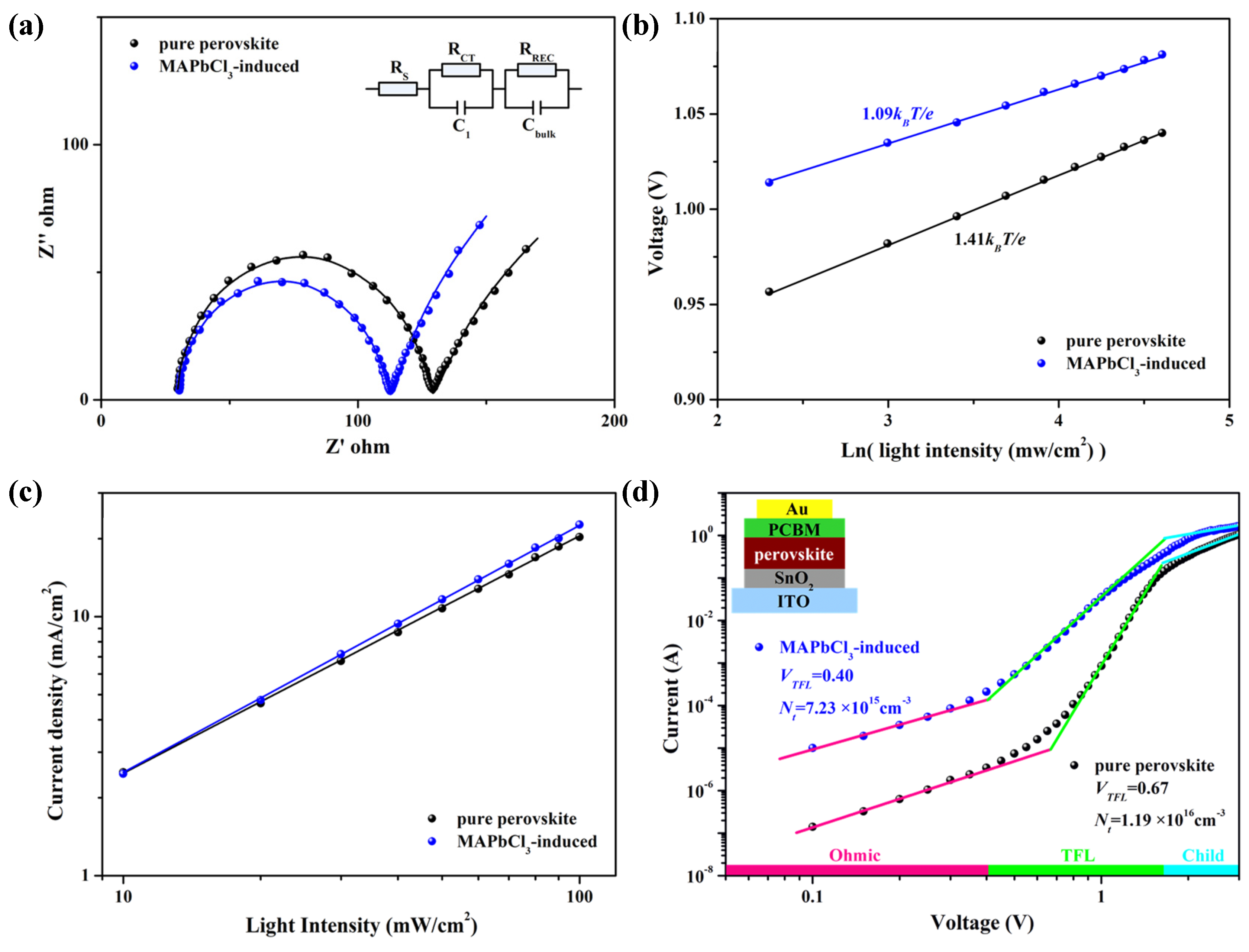
An electrochemical impedance spectroscopy (EIS) was performed to further understand the PCE loss. We performed electrochemical impedance spectroscopy (EIS) measurements to gain more insight into carrier transport and recombination.
Figure 7a shows the Nyquist plots of pure perovskite and MAPbCl
3-induced devices at a bias voltage of 0.8
. The typical two semicircles in perovskite solar cells can be observed: the charge transfer process between the perovskite and the carrier transport layer corresponds to the small semicircle in the high-frequency region. In contrast, the transport–recombination process of the carrier in the perovskite film corresponds to the large semicircle in the low-frequency region [
33]. The resistance of the electrode and the external circuit is reflected by the series resistance (
RS). The values of
RS, transfer resistance (
RCT), and charge recombination resistance (
RREC) are listed in
Table S1, which were obtained by fitting from the equivalent circuit model. From
Table S1, the
RS values are similar but inconsistent with the same structures of the two devices. The
RCT of the MAPbCl
3-induced device is lower than that of the pure device, indicating that the former has a stronger charge transfer capability at the interface, which may lead to an increase in FF, as shown in
Figure 4. Similarly, the MAPbCl
3-induced device has a higher
RREC, indicating that charge recombination is effectively inhibited, which may lead to an increase in
.
Figure 7b shows the relationship between the
Voc and light intensity of the pure perovskite and MAPbCl
3-induced films, which usually follows the equation below [
34]
where
,
,
,
, and
represent the ideality factor, Boltzmann constant, electron charge, absolute temperature, and light intensity, respectively. From the equation, there is a linear relationship between
and light intensity
, and the fitted value of the ideality factor is generally between 1 and 3. When
approaches 1, it indicates that the recombination mechanism in the device is bimolecular recombination. When it is close to 2, it reflects the existence of defect-assisted recombination in the device [
35]. As shown in
Figure 6b, the ideality factor of the MAPbCl
3-induced device is 1.19, which is lower than 1.48 of the pure perovskite device. It is proved that the defect density content in the MAPbCl
3-induced device is low and that the composite method of the device is mainly bimolecular.
Figure 7c shows the relationship between the
values of the pure perovskite and MAPbCl
3-induced devices and light intensity under short-circuit conditions. At a slope of 1, bimolecular recombination at the interface is completely suppressed. Compared with the slope of the pure perovskite device (0.916), the slope of the MAPbCl
3-indued device (0.953) is closer to 1, which indicates that the addition of MAPbCl
3 will inhibit the bimolecular recombination at the interface [
36]. Combined with the EIS results, it may be speculated that defects at the surface and interface may be reduced in the MAPbCl
3-induced perovskite film.
Thus, space–charge limited current (SCLC) measurements can further quantify the trap density in perovskite films. Samples with the structure of ITO/SnO
2/perovskite/PCBM/Au were prepared, as shown in
Figure 7d. The linear region at low bias voltage corresponds to the ohmic response. This is followed by the middle trap-fill-limited (TFL) area. The trap states are filled by the injected carriers in this region. The intersection point between the two regions defines the tarp-filled-limit voltage (
). The relationship between
and trap density (
) is given by the following equation [
37,
38]:
where
,
,
and
0 are the electron charge, perovskite film thickness, relative permittivity of perovskite, and vacuum permittivity, respectively. The
J-V curves of the pure perovskite and MAPbCl
3-induced pure photoelectric devices are shown in
Figure 7d. The calculated trap density of the pure perovskite film is 1.93 × 10
16 cm
−3, which is significantly higher than 7.75 × 10
15 cm
−3 for the MAPbCl
3-induced perovskite film. Due to the low Gibbs formation energy, vacancies can be easily formed at the surface/interface of perovskite crystals, which can serve as charge trap sites [
39]. MAPbCl
3 induces an increase in the grain size of perovskite, resulting in a decrease in the crystal surface and surface vacancies, thereby reducing the trap density.


